Journal list menu

 Issue
Issuephysica status solidi (a): Volume 213, Issue 8
2009-2266August 2016
Export Citations
Download PDFs
Cover Picture
Multiple role of dislocations in the heteroepitaxial growth of diamond: A brief review (Phys. Status Solidi A 8∕2016)
- Page: 2009
- First Published: 11 August 2016
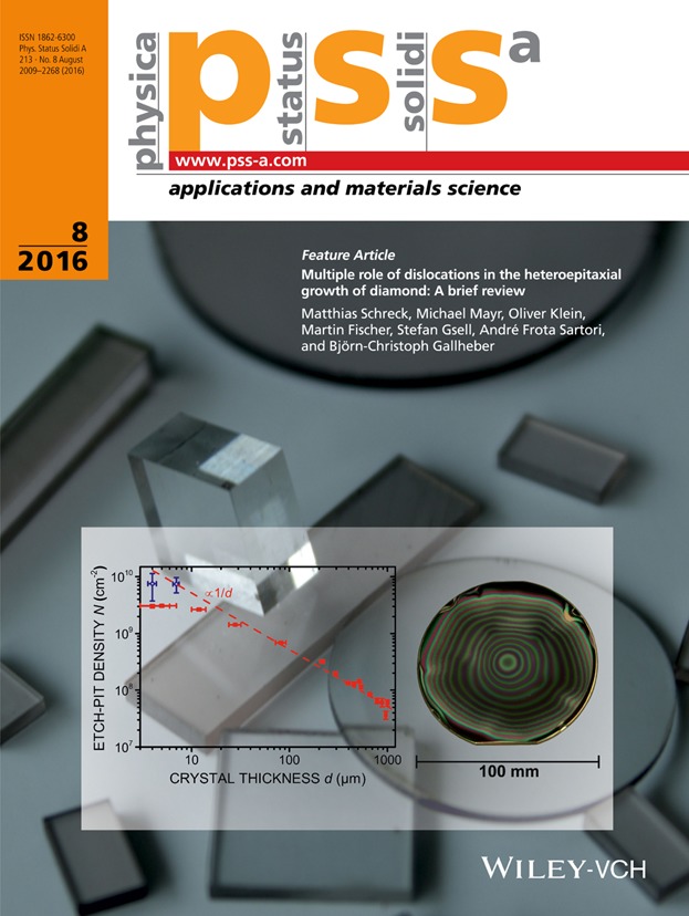
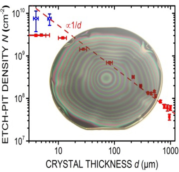
Future success of diamond-based high-power electronic devices critically depends on the availability of wafer-size single crystals. For their realization, heteroepitaxy on iridium is currently the most promising approach in terms of scalability. However, in contrast to homoepitaxial deposition on carefully selected seed crystals, heteroepitaxial diamond layers generally start with a dislocation density of more than 1010 cm−2 and its efficient reduction is the main issue for the subsequent growth of thick high-quality layers. In the Feature Article by M. Schreck et al. (pp. 2028–2035), several different aspects of dislocations in the CVD growth of diamond films are discussed. They comprise the mutual interaction among dislocations, their interaction with the growth surface, the decisive role of dislocations in the formation of growth stress and their role as sinks for dopant atoms. The results provide valuable insights for further efforts in material improvement and the control of stress during film growth. The cover image shows the reduction of dislocation density within the first 1000 ìm of growth and a 4-inch diamond/Ir/YSZ/Si(001) wafer after diamond nucleation and several micron growth. Various cuboids and discs with diameters of up to several centimeters in the background are products synthesized by this technique (www.audiatec.de).
Issue Information
Back Cover
Atmospheric-pressure photoelectron emission from H-terminated and amino-terminated diamond (Phys. Status Solidi A 8∕2016)
- Page: 2268
- First Published: 11 August 2016
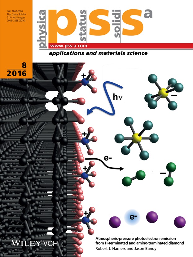
Among diamond's many unusual properties is the ability to act as a negative electron affinity material. While electron emission from diamond has been heavily studied in vacuum, recent work by Hamers and co-workers has shown that diamond can also act as a solid-state emitter of electron in liquids. In their article on pp. 2069−2074, Hamers and Bandy explore the direct emission of electrons into atmospheric-pressure gases, using argon, air, and SF6 as model systems. In contrast to the more commonly used hydrogen-terminated diamond, amineterminated diamond provides a fixed positive surface charge that helps to effectively extract electron from the bulk. Electrons emitted into air and into SF6 can form stable anions (O2 – and SF6 –), leading to electron emission currents controlled by the ion mobilities. In contrast, argon does not form a stable anion, so electrons transported through argon gas are transported as free electrons, albeit subject to frequent scattering events. This work provides new insights into the nature of electron emission from diamond and extends its use as a solid-state emitter of electrons in ambient environments.
Contents
Recent and forthcoming publications in pss
Recent and forthcoming publications in pss
- Page: 2016
- First Published: 11 August 2016
Advanced Materials Physics
Rapid thickness reading of CH3NH3PbI3 nanowire thin films from color maps
- Pages: 2017-2023
- First Published: 29 March 2016

The authors report on a facile, rapid, and calibration-free method to extract automatically the thickness of CH3NH3PbI3 nanowire thin-films on dielectric surfaces directly from optical images. Their method amounts to minimize a suitable defined distance in the red-green-blue color space which measures the difference between the observed and calculated colors of perovskite nanowires.
Dedication
Feature Article
Novel aspects of diamond
Multiple role of dislocations in the heteroepitaxial growth of diamond: A brief review
- Pages: 2028-2035
- First Published: 23 April 2016
For the future, realization of single crystal diamond wafers by heteroepitaxy controlling the dislocations represents a major challenge. In this review the authors highlight different aspects of dislocations in diamond, starting with their visualization, their reduction by annihilation and fusion, their propagation during growth and finally their role in stress formation.
Original Papers
Novel aspects of diamond
Effect of n- and p-type doping concentrations and compensation on the electrical properties of semiconducting diamond
- Pages: 2036-2043
- First Published: 29 July 2016
On the efficiency of combined ion implantation for the creation of near-surface nitrogen-vacancy centers in diamond
- Pages: 2044-2050
- First Published: 18 July 2016
Influence of substrate misorientation on the surface morphology of homoepitaxial diamond (111) films
- Pages: 2051-2055
- First Published: 18 March 2016
Surface-enhanced infrared spectroscopy on boron-doped diamond modified with gold nanoparticles for spectroelectrochemical analysis
- Pages: 2056-2062
- First Published: 16 June 2016
Modification of internal barrier in hydrogen-terminated heavily phosphorus-doped diamond for field emission
- Pages: 2063-2068
- First Published: 19 June 2016
Atmospheric-pressure photoelectron emission from H-terminated and amino-terminated diamond
- Pages: 2069-2074
- First Published: 28 April 2016
Diamond on aluminum nitride as a platform for integrated photonic circuits
- Pages: 2075-2080
- First Published: 15 June 2016
Recovery of copper from dilute cupric sulfate solution by electrodeposition method using boron-doped diamond electrodes
- Pages: 2081-2086
- First Published: 22 June 2016
Assessment of heterogeneous electron-transfer rate constants for soluble redox analytes at tetrahedral amorphous carbon, boron-doped diamond, and glassy carbon electrodes
- Pages: 2087-2098
- First Published: 20 July 2016
The effect of surface termination on glucose oxidation using Ni-modified diamond electrodes
- Pages: 2099-2104
- First Published: 10 May 2016
A theoretical study of dye molecules adsorbed onto diamond (111) surfaces
- Pages: 2105-2111
- First Published: 25 July 2016
Hydrophobic/lipophilic nanodiamond particles fabricated by surface modification with 1-octadecene
- Pages: 2112-2116
- First Published: 16 June 2016
Mid-infrared thin-film diamond waveguides combined with tunable quantum cascade lasers for analyzing the secondary structure of proteins
- Pages: 2117-2123
- First Published: 28 April 2016
pH-responsive phenylboronic acid-modified diamond particles: Switch in carbohydrate capture ability triggers modulation of physicochemical and lectin-recognition properties
- Pages: 2124-2130
- First Published: 28 June 2016
The effect of carboxylated nanodiamond (cNDs) on the migration of HepG2 cells
- Pages: 2131-2137
- First Published: 09 April 2016
Expert Opinion
Novel aspects of diamond
Toward a golden standard in single digit detonation nanodiamond
- Pages: 2138-2145
- First Published: 30 June 2016
Original Papers
Regular contributions
Investigation of rare-earth metal-doped Ba0.96Sr0.04Zr0.04Ti0.96O3 ceramics
- Pages: 2147-2151
- First Published: 22 February 2016
Random and correlated damage initiation in impact-loaded SiC ceramics
- Pages: 2152-2155
- First Published: 22 February 2016
Observations of stress accumulation and relaxation in solid-state lithiation and delithiation of suspended Si microcantilevers
- Pages: 2156-2168
- First Published: 23 February 2016
Monitoring the phase evolution of Cu(In,Ga)Se2 by different Se flux via in-situ XRD
- Pages: 2169-2175
- First Published: 26 February 2016
Improvement in thermoelectric performance of In6Se7 by substitution of Sn for In
- Pages: 2176-2182
- First Published: 29 February 2016
Optically modulated resistive switching in BiFeO3 thin film
- Pages: 2183-2188
- First Published: 26 February 2016
Fully inkjet-printed metal-oxide thin-film transistors on plastic
- Pages: 2189-2195
- First Published: 01 March 2016
Independent control of phases and defects in TiO2 thin films for functional transistor channels
- Pages: 2196-2202
- First Published: 02 March 2016
Overcoming the poor crystal quality and DC characteristics of AlGaN/GaN/AlGaN double-heterostructure high electron mobility transistors
- Pages: 2203-2207
- First Published: 04 March 2016
Piezotronic-based magnetoelectric sensor: Fabrication and response
- Pages: 2208-2215
- First Published: 04 March 2016
Deep junction III–V solar cells with enhanced performance
- Pages: 2216-2222
- First Published: 07 March 2016
The effectiveness of electron blocking layer in InGaN-based laser diodes with different indium content
- Pages: 2223-2228
- First Published: 10 March 2016
Cubic-structured tin selenide thin film as a novel solar cell absorber
- Pages: 2229-2236
- First Published: 10 March 2016
Thermal conductivity of bulk boron nitride nanotube sheets and their epoxy-impregnated composites
- Pages: 2237-2242
- First Published: 10 March 2016
Magnetically controlled space charge capacitance at La1−xSrxMnO3/SrxLa1−xTiO3 interfaces
- Pages: 2243-2253
- First Published: 10 March 2016
Dielectric enhancement of PbZr0.3Ti0.7O3/LaNiO3 multilayer thick film
- Pages: 2254-2258
- First Published: 17 March 2016
Low-temperature grown indium oxide nanowire-based antireflection coatings for multi-crystalline silicon solar cells
- Pages: 2259-2263
- First Published: 21 March 2016
Erratum
Regular contributions
Memory effect by charging of ultra-small 2-nm laser-synthesized solution processable Si-nanoparticles embedded in Si–Al2O3–SiO2 structure [Phys. Status Solidi A 212, 1751–1755 (2015)]
- Page: 2264
- First Published: 26 July 2016
Information for authors
Sign up for email alerts
Tools
![]()
In 2022, the youngest family member physica status solidi (RRL) – Rapid Research Letters is turning 15 years. To celebrate this milestone, we present a new virtual collection with invited articles.
![]()
As we celebrate the 60th anniversary year of the physica status solidi family, click here to access our continuously updated collection of invited articles written by authors and partners of the pss journals.