Journal list menu

 Issue
Issuephysica status solidi (a): Volume 220, Issue 16
Special Issue:Nitride Semiconductors
August 2023Guest Editor(s):
Export Citations
Download PDFs
Cover Picture
Characterization of Lateral and Longitudinal Mode Competition in Blue InGaN Broad-Ridge Laser Diodes
- First Published: 18 August 2023

Broad-Ridge Laser Diodes
Longitudinal mode competition in broad ridge laser diodes is affected by different lateral modes occupying longitudinal mode clusters at different wavelengths. Here, mode competition causes anti-phased oscillations between these wavelength clusters – and simultaneously between different lateral modes. In article number 2200751, Lukas Uhlig, Dominic J. Kunzmann, and Ulrich T. Schwarz investigate the current-dependent mode distribution, oscillation frequencies, and the stability of the phase relation as an indicator for the coupling strength between mode clusters.
Inside Front Cover
Power Performance of AlGaN/GaN High-Electron-Mobility Transistors with AlN Buffer on SiC Substrate at 3.5 GHz
- First Published: 18 August 2023
Power Performance of AlGaN/GaN HEMTs
In article number 2200826, Okhyun Nam and colleagues present the power performance of an AlGaN/GaN HEMT with AlN buffer on a 4-inch SiC substrate, grown by high-temperature metalorganic chemical vapor deposition. The fabricated devices were examined and showed positive characteristics, such as low slump ratio and breakdown voltage. The results demonstrate the potential of using an AlN buffer HEMT in high-power RF devices of the future.
Masthead
Inside Back Cover
DC and Pulse I–V Characteristics of Strain-Engineered AlGaInN/GaN HEMTs fabricated on Single-Crystal AlN Substrate
- First Published: 18 August 2023
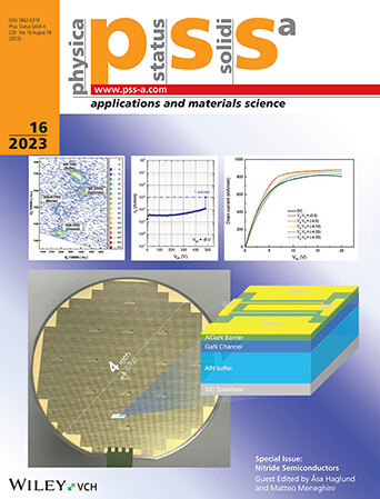
DC and Pulse I–V Characteristics of AlGaInN/GaN HEMTs
In article number 2200733, Makoto Miyoshi and colleagues use MOVCD to grow a GaN HEMT structure with a strain-engineered AlGaInN barrier layer on a single-crystal AlN substrate. The on-wafer device evaluation results show good DC and pulse I–V characteristics without large negative resistance even at high current operations.
Back Cover
Recent Progress of E-mode Gallium Nitride Metal–Insulator–Semiconductor -High Electron Mobility Transistors with Hybrid Ferroelectric Charge Trap Gate (FEG-HEMT) for Power Switching Applications
- First Published: 18 August 2023

Hybrid FEG-HEMTs
The high-performance hybrid ferroelectric charge storage gate (FEG) GaN HEMT has gradually gained attention due to the concept being a useful tool to realize E-mode operations. In article number 2300018, the NYCU group in Taiwan led by Edward Yi Chang has shown that implementing an additional ferroelectric layer on top of the charge storage layer demonstrates exceptional electrical characteristics and shows great potential for future power switching applications.
Guest Editorial
Review
Recent Progress of E-mode Gallium Nitride Metal–Insulator–Semiconductor -High Electron Mobility Transistors with Hybrid Ferroelectric Charge Trap Gate (FEG-HEMT) for Power Switching Applications
- First Published: 30 March 2023
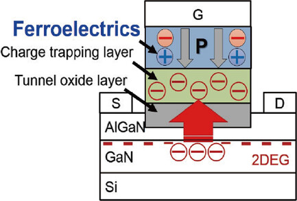
The high-performance ferroelectric charge storage gate (FEG) gallium nitride high-electron-mobility transistors (HEMT) has gradually gained attention due to the concept being a useful tool to realize E-mode operations, which has been a focused topic in recent years for their potential applications. This article attempts to review the latest progress in this technology, including alternative improvements and device characteristics.
Research Articles
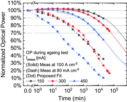
Defect Dynamics and Internal Quantum Efficiency Decay Resultant Ultraviolet C-Band Light-Emitting Diode Lifetime Performance
- First Published: 08 September 2022
A light-emitting diode (LED) lifetime model is proposed, which fits excellently well to full sets of lifetime measurement data due to internal quantum efficiency (IQE) degradation. Using the model, a lifetime of ≈96 000 h is projected to maintain 70% of the initial optical output power for an ultraviolet C-band LED based on a stress test for ≈10 000 h.
Impact of the Channel Thickness on Electron Confinement in MOCVD-Grown High Breakdown Buffer-Free AlGaN/GaN Heterostructures
- First Published: 29 September 2022
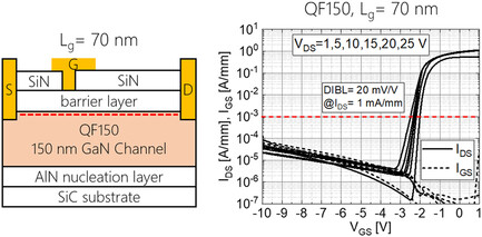
A buffer-free epi-structure, QuanFINE, with the reducing GaN channel thickness from 250 to 150 nm is grown directly on the AlN nucleation layer without apparent degradation of crystal structural quality. An excellent drain-induced barrier lowering of 20 mV V−1 and an outstanding critical electric field of 0.95 MV cm−1 are demonstrated. Moreover, GaN channel thickness dependence of device performance is investigated.
A Combination of Ion Implantation and High-Temperature Annealing: The Origin of the 265 nm Absorption in AlN
- First Published: 25 September 2022

The commonly observed absorption around 265 nm in AlN is hampering the outcoupling efficiency of light-emitting diodes (LEDs) emitting in the UV-C regime. A specially tailored experiment using a combination on ion implantation with subsequent high-temperature annealing opens the interpretation of UV absorption for a revision and questions the role of carbon in the 265 nm absorption band.
Radiative Recombination and Carrier Injection Efficiencies in 265 nm Deep Ultraviolet Light-Emitting Diodes Grown on AlN/Sapphire Templates with Different Defect Densities
- First Published: 08 October 2022

Herein, 265 nm deep ultraviolet light-emitting diodes (DUV LEDs) grown on three different AlN/sapphire templates are investigated. The external quantum efficiency (EQE) of each individual device is separated into maximum radiative recombination (RRE), carrier injection (CIE), and light extraction efficiency. The results show that for DUV LEDs, CIE is ≈50% and limits EQE to a similar extent as RRE.
Suppression of Impact Ionization by Carbon Doping in the GaN Buffer Layer in InAlN/GaN-Based High Electron Mobility Transistors
- First Published: 24 November 2022

Impact ionization in InAlN/GaN high electron mobility transistors (HEMTs) is studied. The bell-shaped nature of the IG–VGS characteristics proves the occurrence of impact ionization in HEMT without carbon doping in the GaN buffer layer. It is shown that carbon-doped buffer layer reduces impact ionization by reducing the electric field at the drain side gate edge.
Highly Si-Doped GaN Regrown by Metal–Organic Vapor-Phase Epitaxy for Ohmic Contact Applied to Quaternary Barrier-Based High-Electron-Mobility Transistors
- First Published: 23 November 2022
The regrowth of an ohmic contact at 850 °C by metal–organic vapor-phase epitaxy is conducted by carrier gas switching techniques to achieve selectivity and homogeneous thickness. A high aperture ratio in the dielectric mask is a key factor to control the growth rate and high doping level. 0.26 Ω mm low contact resistance is obtained.
Extraction and Optimization of Compact Drain Current Model Parameters for GaN High-Electron-Mobility Transistors
- First Published: 23 November 2022

A good match between the model and experimental data is shown, after extracting and optimizing the complete DC model parameters set of GaN-based high-electron-mobility transistors (HEMTs). The results show a good match for both micrometer and sub-micrometer gate lengths. The optimizer, namely, the Levenberg–Marquardt algorithm, is the key to better accuracy.
Low-Temperature Electrical Transport Properties of Molecular Beam Epitaxy-Grown Mg-Doped GaN Subjected to a High-Temperature Annealing Process
- First Published: 31 December 2022
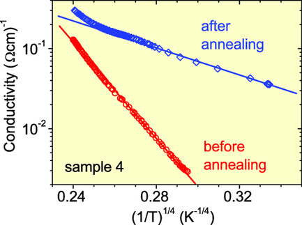
Contrary to generally accepted opinion, thermal annealing of molecular beam epitaxy-grown GaN:Mg material allows to increase distinctly the hole concentration. Moreover, the electrical properties, sensitive to this procedure, show the hopping effects near room temperature. This fact is very important for crystal growers, because it may lead to erroneous conclusions about the carrier concentration as a function of technological process parameters.
Characterization of Lateral and Longitudinal Mode Competition in Blue InGaN Broad-Ridge Laser Diodes
- First Published: 01 December 2022

Laser diodes show dynamic mode competition that causes cyclic variations in the laser spectrum in the frequency range of 50–100 MHz. In broad-ridge laser diodes, lateral modes of different order occupy separate spectral clusters and take part in mode competition. Coupling between lateral modes is investigated in terms of frequency and phase difference of mode competition effects.
Analysis of Mechanical Strain in AlGaN/GaN HFETs
- First Published: 31 December 2022
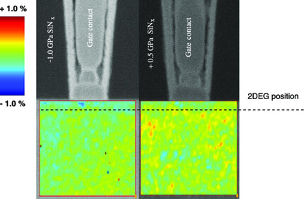
Using nano-beam electron diffraction strain measurements, quantitative correlation between microscopic strain dissimilarity (0.23%) in epitaxial layers with 1.5 GPa variation of intrinsic stress in passivation layer and 1.4-V threshold voltage shift in transistors is provided. Based on that, various mechanisms contributing to Vth shift are distinguished. Herein, the way is paved for future optimization/realization of strain-engineered GaN-based devices.
DC and Pulse I–V Characteristics of Strain-Engineered AlGaInN/GaN HEMTs fabricated on Single-Crystal AlN Substrate
- First Published: 13 January 2023
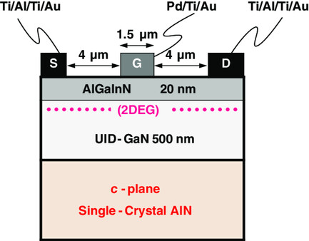
A GaN high-electron-mobility transistor (HEMT) structure consisting of a strain-engineered quaternary AlGaInN barrier layer on a 500 nm thick unintentionally doped (UID)–GaN channel layer is grown on a single-crystal AlN substrate by metal–organic chemical vapor deposition (MOCVD) and subjected to the device fabrication and characterization. The on-wafer device evaluation results provide good DC and pulse current–voltage (I–V) characteristics without large negative resistance even at high-current operations.
Effect of Poly-Crystallinity on the Magnetoelectric Behavior of TiN/AlN/Ni MEMS Cantilevers Investigated by Finite Element Methods
- First Published: 13 January 2023
The polycrystalline nature of experimental magnetoelectric MEMS sensors leads to different anisotropic contributions of individual grain orientations and aspects. As a consequence, the vibrational properties of MEMS sensors are affected resulting in a superposition of the individual anisotropic ΔE effects. Herein, sensors based on TiN/AlN/Ni cantilevers are investigated in regard of the ΔE effect and the derived sensitivity.
2.2 W/mm at 94 GHz in AlN/GaN/AlN High-Electron-Mobility Transistors on SiC
- First Published: 16 January 2023

Aluminum nitride (AlN) offers novel potential for electronic integration and performance benefits for high-power, millimeter-wave amplification. When tuned for peak power-added efficiency (PAE), the presented AlN/GaN/AlN high-electron-mobility transistors show PAE of 25% and 15%, with associated output power (Pout) of 2.5 and 1.7 W mm−1, at 30 and 94 GHz, respectively.
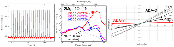
A Combination of Ion Implantation and High-Temperature Annealing: Donor–Acceptor Pairs in Carbon-Implanted AlN
- First Published: 14 February 2023
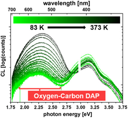
A donor–acceptor pair transition in aluminum nitride is identified, probably between the most abundant impurities during crystal growth: carbon and oxygen. High concentrations of both species are realized by ion implantation and diffusion during annealing. The identification is based on continuous-wave and time-resolved cathodoluminescence measurements at low and high temperatures plus theoretical considerations.
Metal Stop Laser Drilling for Blind via Holes of GaN-on-GaN Devices
- First Published: 01 March 2023
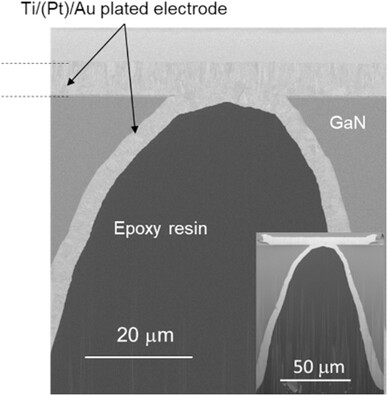
The metal stop laser drilling for through-substrate vias of GaN-on-GaN GaN high-electron-mobility transistors (HEMTs) is reported using a UV sub-nanosecond laser as a light source. By monitoring the Bremsstrahlung emission at the drilling point, a metal stop with a precision higher than 1 μm is achieved. A through-substrate electrode with a resistance of less than 5 mΩ is demonstrated.
Compositional Mapping of the AlGaN Alloy Composition in Graded Buffer Structures Using Cathodoluminescence
- First Published: 15 February 2023
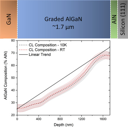
Facilitated by their growth on silicon substrates, the III-nitride semiconductor system has played a crucial role in the success of next-generation power electronic devices. However, this technology faces significant challenges relating to the buffer layers. By utilizing the high spectral and spatial resolutions of cathodoluminescence, herein, a novel method of quantifying alloy compositions in graded AlGaN buffer layers is presented.
Electrical Characteristics of Gated Anode Diodes Based on Normally Off Recessed-Gate GaN High-Electron-Mobility Transistors for Rectenna Applications
- First Published: 03 March 2023

GaN high-electron-mobility transistor (HEMT)-based gated-anode diodes (GADs) for 5.8 GHz high-power rectenna application are proposed. Using HEMTs with a recessed gate structure, the GAD significantly improves maximum anode forward current and reverse breakdown voltage simultaneously. Rectifying performance simulated with SPICE model shows that the GAD is a promising device for high-power rectenna at 5.8 GHz.
Vertical GaN Transistor with Semi-Insulating Channel
- First Published: 15 March 2023

Herein, a novel concept of vertical GaN transistors having semi-insulating GaN channel is demonstrated. Robust layout of the device, missing p-type doping, perspective scalability of the breakdown voltage without compromising n-type doping in the drift region, and high electron mobility in the channel may be the main assets of the approach.
Avoiding Gallium Pollution in Close-Coupled Showerhead Reactors, Alternative Process Routes
- First Published: 03 March 2023

Herein, a model for unintentional gallium integration into InAlN films is proposed, and process modifications are investigated to reduce this unwanted effect. Different approaches such as reduction in GaN growth temperature and growth of AlGaN films result in significant reductions to the gallium incorporated, and suggest pathways for further optimization for growth of InAlN layers for high-electron-mobility transistors devices.
High-Resolution Investigation of a Grating-Stabilized Laser with a Fabry–Pérot Interferometer
- First Published: 10 March 2023

Narrow-linewidth lasers are used for many applications for example quantum computing. A self-built external cavity diode laser in single-mode operation is shown and investigated with a Fabry–Pérot interferometer. With increasing current the wavelength shifts to longer wavelengths and two different slopes are visible. Both shifts correspond to a change in the refractive index and are differentiated with the FPI.
Submicrometer-Thick Step-Graded AlGaN Buffer on Silicon with a High-Buffer Breakdown Field
- First Published: 16 March 2023
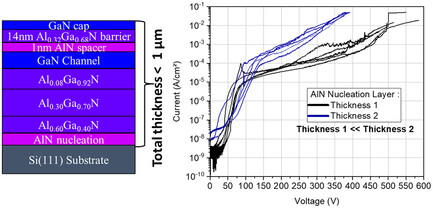
A submicrometer-thick step-graded AlGaN buffer is grown on Si by ammonia-molecular beam epitaxy (NH3-MBE). An outstanding vertical buffer breakdown field of 6 MV cm−1 is demonstrated. Moreover, DC and large signal characteristics for 100 nm gate length show high electron confinement under high electric field enabling operation under high drain bias at high frequency with high robustness.
Electrical Behavior of Vertical Pt/Au Schottky Diodes on GaN Homoepitaxy
- First Published: 30 March 2023

I–V characteristics investigation in the function of temperature shows barrier height inhomogeneities for vertical GaN Schottky diodes. These inhomogeneities are a common and crucial issue for power device application. Their potential origin (strain, doping variation, electrically active defects) is studied using Raman spectroscopy and deep-level transient spectroscopy.
Highly Sensitive Hydrogen Sulfide Sensor Based on GaN/GaInN Heterostructure
- First Published: 24 March 2023
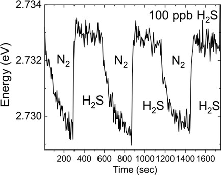
GaInN heterostructure sensors are optimized primarily for hydrogen sulfide sensing. Thin GaN cap layer, thick GaInN quantum well (QW), and low-doping concentration with a gold functionalization layer are found to be better for sensitivity in the 10–100 parts per billion (ppb) range. Ammonia gas is also detected in the 5–10 ppm range.
Novel Codoping Moiety to Achieve Enhanced P-Type Doping in GaN by Ion Implantation
- First Published: 16 March 2023
Codoping of gallium nitride for improved acceptor ionization has long been theorized; here we show significantly improved p-type doping of GaN with donor coimplantation for formation of low-activation energy complexes. Transmission line measurements, photoluminescence, and p-type hall exhibit vast improvement with additional oxygen donors compared to silicon having significant implications for device topologies requiring colocated dopants or utilizing n-polar material.
Realization of Low Dislocation Density AlN on Patterned Sapphire Substrate by Hydride Vapor-Phase Epitaxy for Deep Ultraviolet Light-Emitting Diodes
- First Published: 30 March 2023

By introducing the hole-type patterned sapphire substrate (HPSS) with a properly designed pattern configuration as a substrate for AlN growth, threading dislocation density (TDD) is significantly lowered from 1.48 × 10⁹ to 4.38 × 108 cm−2. The TDs on the mesa zones generated at AlN/sapphire interface can be effectively suppressed by bending toward coalescence zone during the subsequent lateral overgrowth.
Performance of Ultraviolet-B Laser Diodes on AlGaN Templates Prepared Using Different Fabrication Methods
- First Published: 03 March 2023

AlGaN templates are fabricated using the spontaneous nucleation and AlN nanopillar methods, and ultraviolet-B (UV-B) laser diodes (LDs) with the same structure are fabricated on them. Herein, three and six times higher values for Sd and Ppeak are confirmed, respectively, using templates fabricated using the AlN nanopillar method. The method of AlN nanopillars is realized by high-performance UV-B LDs.
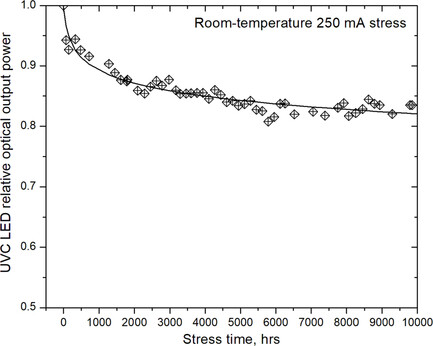
Performance and Degradation of Commercial Ultraviolet-C Light-Emitting Diodes for Disinfection Purposes
- First Published: 13 April 2023
The reliability of ultraviolet-C (UV-C) light-emitting diodes (LEDs) is crucial for next-generation disinfection systems. Herein, the electrical, optical, and spectral properties of UV-C LEDs with an emission peak of 275 nm during their lifetime are analyzed. The analysis allows to determine the optimal balance between performance, reliability, and costs in a solid-state disinfection system.
Suppression of Reverse Leakage in Enhancement-Mode GaN High-Electron-Mobility Transistor by Extended PGaN Technology
- First Published: 18 April 2023
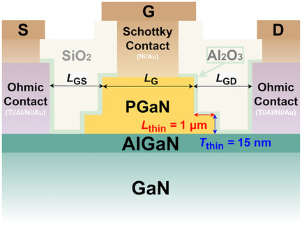
An extended PGaN gate structure that can reduce the peak electric field is proposed and successfully adopted on a Schottky PGaN enhancement-mode GaN high-electron-mobility transistor platform. The device features a saturation current of 256 mA mm−1, a threshold voltage of +1.8 V, and an ON-resistance of 19.781 Ω mm.
Bright Emission at Reverse Bias After Trailing Edge of Driving Pulse in Wide InGaN Quantum Wells
- First Published: 21 April 2023
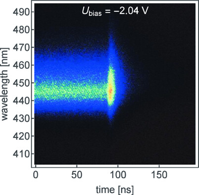
Laser diodes with different InGaN quantum well thicknesses up to 25 nm are analyzed. Efficient screening of the piezoelectric field and excited-state operation are reported. The time-dependent behavior below threshold gives insights about the quantum well tilt and the wave function overlap. A sharp intensity increase and wavelength shift are observed at the end of the pulse.
Power Performance of AlGaN/GaN High-Electron-Mobility Transistors with AlN Buffer on SiC Substrate at 3.5 GHz
- First Published: 20 April 2023
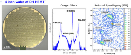
Herein, the power performance of an AlGaN/GaN high-electron-mobility transistor (HEMT) with AlN buffer on SiC substrate, grown by high-temperature metal–organic chemical vapor deposition, is presented. The fabricated devices are examined and show positive characteristics, such as low slump ratio and breakdown voltage. The potential of using an AlN buffer HEMT is demonstrated by the results for use in high-power radio-frequency devices of the future.
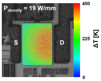
Effect of GaN/AlGaN Buffer Thickness on the Electrothermal Performance of AlGaN/GaN High Electron Mobility Transistors on Engineered Substrates
- First Published: 20 April 2023
AlGaN/GaN high electron mobility transistors (HEMTs) on engineered substrates are grown with different GaN/AlGaN buffer layer thickness and evaluated via atomic force microscopy, high-resolution X-ray diffraction, Raman spectroscopy, and steady-state thermoreflectance. Fabricated HEMTs are evaluated via DC and pulsed electrical techniques and thermoreflectance imaging. It is reported that these HEMTs exhibit high GaN quality, low stress, low current collapse, and low thermal resistance.
Fabrication of Low On-Resistance and Normally Off AlGaN/GaN Metal Oxide Semiconductor Heterojunction Field-Effect Transistors with AlGaN Back Barrier by the Selective Area Regrowth Technique
- First Published: 25 April 2023
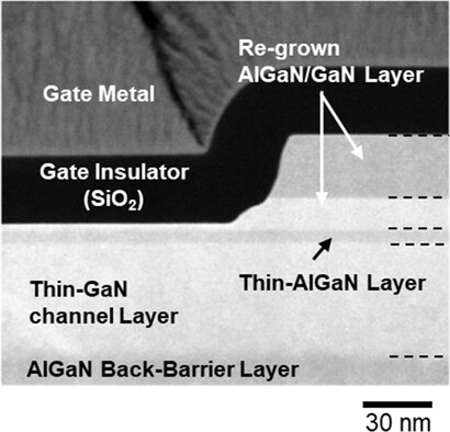
Cross-sectional transmission electron microscope (TEM) images of the recessed-gate structure on a thin AlGaN/GaN channel metal oxide semiconductor heterojunction field-effect transistor fabricated by selective area regrowth. The thin AlGaN/GaN channel with an AlGaN back barrier and the regrown AlGaN/GaN high electron mobility transistor structure provides low on-resistance and normally off operation.
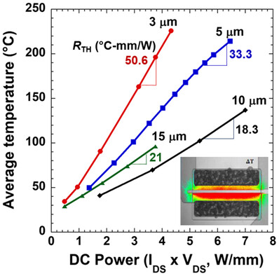
Electrothermal Performance of AlGaN/GaN Lateral Transistors with >10 μm Thick GaN Buffer on 200 mm Diameter-Engineered Substrates
- First Published: 03 May 2023
AlGaN/GaN lateral transistors fabricated with >10 μm thick buffers on 200 mm diameter-engineered substrates are demonstrated. The engineered substrates result in minimal residual stress in the GaN buffer while the fabricated transistors display both electrical and thermal performance competitive with other substrate technologies such as Si. A pathway for large-scale production of high-yield GaN devices is presented.
Investigation of Electrical Properties of N-Polar AlGaN/AlN Heterostructure Field-Effect Transistors
- First Published: 16 May 2023
Herein, N-polar Al0.1Ga0.9 N/Al0.9Ga0.1 N/AlN field-effect transistor (FET) is fabricated using metal–organic vapor-phase epitaxy, and the static FET operation is confirmed to exhibit an n-channel and pinch-off.
Development of High-Reflectivity and Antireflection Dielectric Multilayer Mirrors for AlGaN-Based Ultraviolet-B Laser Diodes and their Device Applications
- First Published: 28 May 2023
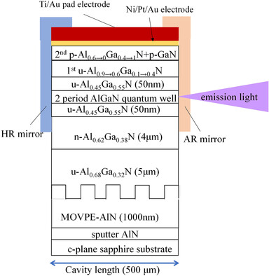
Fabrication techniques for high-reflectivity (HR) and antireflection (AR) dielectric multilayer mirrors for AlGaN-based ultraviolet-B (UV-B) laser diodes are developed. By mounting those mirrors on both edges of the device, the improvement of device performance is confirmed, such as increased light output and slope efficiency.
Metal–Organic Chemical Vapor Deposition-Grown AlScN for Microelectromechanical-Based Acoustic Filter Applications
- First Published: 12 June 2023
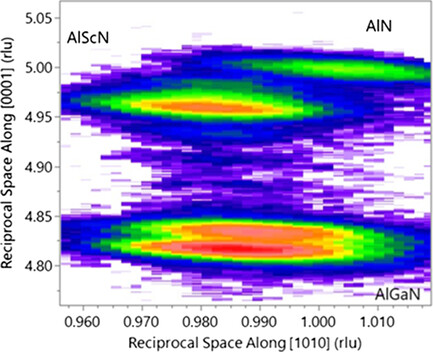
Piezoelectric AlScN single-crystal films deposited by metal–organic chemical vapor deposition are used for the first time in the fabrication of bulk acoustic wave filters. The effects of growth conditions are discussed and novel structures are produced to manage internal stresses and preserve planar surface morphology.
Comparative Performance Evaluation for 1.2–10kV Conventional and Superjunction GaN Current Aperture Vertical Electron Transistors
- First Published: 13 June 2023

The performance potentials and limits for GaN current aperture vertical electron transistors with conventional, doped, and natural polarization (PSJ) superjunction drift layers at 1.2–10 kV BV ratings are quantitively compared by extracting their static and dynamic performance parameters using technology computer-aided design simulation. PSJ offers the best performance with at least 22% and 80% at 1.2 and 10 kV respectively.
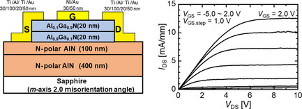
Si-Doping Effects in AlGaN Channel Layer on Performance of N-Polar AlGaN/AlN FETs
- First Published: 15 July 2023
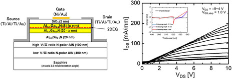
AlN substrate offers various advantages, such as high breakdown voltage and high-temperature operation. Herein, a N-polar AlGaN/AlN-heterostructured field-effect transistor (FET) with static FET characteristics is successfully fabricated. However, the drain current density, IDS, remains significantly small. This study aims to improve IDS by doping Si in the topmost AlGaN channel layer under various conditions.
Sign up for email alerts
Tools
![]()
In 2022, the youngest family member physica status solidi (RRL) – Rapid Research Letters is turning 15 years. To celebrate this milestone, we present a new virtual collection with invited articles.
![]()
As we celebrate the 60th anniversary year of the physica status solidi family, click here to access our continuously updated collection of invited articles written by authors and partners of the pss journals.