A Combination of Ion Implantation and High-Temperature Annealing: Donor–Acceptor Pairs in Carbon-Implanted AlN
Abstract
Herein, carbon-implanted high-temperature annealed (HTA) AlN layers are analyzed and donor–acceptor pair (DAP) transitions probably between the two most abundant impurities, carbon and oxygen, are identified. Both are regarded as the main, hard-to-avoid impurities in crystal growth. Oxygen is believed to lead to absorption in the deep UV below a wavelength of 250 nm. In contrast, carbon is the most likely candidate to be responsible for a distinct absorption band around 265 nm. This interpretation has recently been challenged. In this study, carbon-implanted and HTA AlN layers with ion fluences above 8.1 × 1015 cm−2 are analyzed using low-temperature and time-resolved cathodoluminescence spectroscopy. Due to the high concentration of oxygen inside the AlN, as a result of the HTA process, a DAP transition between a most likely carbon-related acceptor and ON is observed. The measured temperature- and power-dependent blueshift of the peak emission energy as well as the luminescence transients can be clearly explained by a continuous change from a DAP transition at low temperature to a free electron to acceptor transition with increasing temperature. The findings are supported by a configurational coordinate model that describes the measured behavior qualitatively.
1 Introduction
Over the last decades, light-emitting diodes (LEDs) and laser diodes (LDs) based on nitride semiconductors were notably developed and industrialized, allowing broad commercial utilization. In addition to the highly optimized blue-emitting LEDs and infrared LDs based on traditional III–V semiconductors, emitters for the UV range made of aluminum gallium nitride (AlGaN) received great interest lately.[ 1, 2 ] The bandgap of Al x Ga1−x N can be tuned between roughly 6.2 and 3.4 eV by changing the aluminum-to-gallium ratio. These high bandgap energies give rise to a multitude of different possible defect-related energy states inside it, reducing the radiative recombination efficiency and leading to unwanted luminescence signals at wavelengths corresponding to the energetic levels of the defect states.[ 3, 4 ]
A broad range of possible defects in AlN has been identified in previous studies, as summarized by Koppe et al.[ 3 ] Many publications focus on the experimental or theoretical characterization of these defects and possible energetic transitions involving them. In the early phases of research on AlN, many results were based on the luminescence behavior of powder samples with extremely high impurity concentrations compared to semiconductor standards, most notably oxygen, and transition metals from sintering aids like yttrium oxide.[ 5 ] Thus, the results of different groups are hard to compare, as the impurity or defect landscape may vary drastically, depending on the fabrication technique of the AlN crystal, process parameters, and the base materials used. This is especially the case if more than one impurity or defect are involved in the transition: For example, a donor–acceptor pair (DAP), whose emission energy depends on the concentration (i.e., the distance between a single pair) of the involved defects.[ 6 ] The two most abundant impurities, oxygen and carbon, as well as related defect complexes together with intrinsic point defects like vacancies were discussed in detail.[ 5, 7-12 ] Typically, such defects are studied using, for example, cathodoluminescence (CL) spectroscopy, photoluminescence (PL) spectroscopy, and related measurement techniques. There are also reports about DAP transitions between carbon-related defects and different donor states present in the literature.[ 13, 14 ] As a complementary technique, the defect-related absorption can be measured using standard techniques like UV–vis absorption spectroscopy, absorption measurements in PL setups, or photoluminescence-excitation (PLE) measurements. Density functional theory (DFT) calculations often complement the experiments by adding a microscopic model that allows studying the crystal on a fundamental base, for example, obtaining information about the electron–phonon coupling at the respective defect.[ 4, 15 ]
AlN crystals can be grown by a wide range of different techniques such as physical vapor transport (PVT), metalorganic vapor phase epitaxy (MOVPE), physical vapor deposition (PVD), and hydride vapor phase epitaxy (HVPE).[ 2, 16 ] Recently, the recrystallization of submicron thick AlN/sapphire templates using high-temperature annealing (HTA) has gained a lot of interest as a means of manufacturing epitaxial layers with a very high crystallinity. These thin layers are typically deposited using PVD or MOVPE processes and afterward recrystallized at high annealing temperatures of up to 1700 °C, as first introduced by Fukuyama et al., who employed an N2–CO atmosphere to prevent decomposition.[ 17 ] Shortly after, Miyake et al. introduced a refined technique, the so-called face-to-face approach in pure N2 atmosphere.[ 18 ] Like shown recently, HTA is also a suited technique to anneal intrinsic point defects in AlN introduced via ion implantation, like Frenkel pairs or, in general, vacancies and interstitials.[ 19 ]
UV-C LEDs for disinfection/sterilization purposes exhibit the largest germicidal efficacy around an emission wavelength of 265 nm.[ 1 ] Coincidentally, AlN possesses a prominent absorption line at a photon wavelength of 265 nm (corresponding to ≈4.7 eV photon energy), which is hampering the efficiency of these UV-C LEDs. Until recently, in most researchers’ opinion, this was closely linked to the incorporation of excessive amounts of carbon into the crystal during its growth.[ 8, 20-22 ] In an earlier publication, by the combination of ion implantation and HTA, we proposed VN as the absorbing point defect causing the 265 nm absorption in AlN.[ 19 ] In our previous study, we implanted carbon among other species to adjust the impurity levels and point defect concentration in AlN thin films. The results prompted a reevaluation of the role of carbon impurities and their effect on the optical properties of AlN.
As CN does not seem to be responsible for the 265 nm absorption in AlN, emission bands, which are presently assumed to be related to carbon, should also be thoroughly revisited. Therefore, we report here on detailed CL investigations of AlN samples that were implanted with different fluences of carbon and annealed afterward at a temperature of 1700 °C. The annealing process is a well-suited technique to cure the implantation damage and is expected to lead to an incorporation of carbon into the nitrogen sublattice of AlN. Additionally, the abundance of oxygen in HTA AlN leads to a favored incorporation of ON instead of VN due to lower formation energy, which allows us to separate between the implanted carbon and VN that may form as a compensating donor during a process that involves enough thermal energy to be seen close to thermodynamic equilibrium and lacks the supply of oxygen.[ 23, 24 ]
Here, the presented luminescence data were acquired in a temperature range between 20 and 373 K. Our cw-CL results are supported by time-resolved CL (TRCL), secondary-ion mass spectroscopy (SIMS) measurements, high-resolution X-ray diffraction (HRXRD) data, and Monte-Carlo simulations of the implantation.
2 Experimental Section
Nominally, 300 nm thick commercial AlN samples grown by PVD on c-oriented sapphire substrates were used for the experiments. The as-grown Al-polar samples exhibited a nanocolumnar morphology with c-oriented grains of ≈25 nm diameter. The (0002) and (10-12) reflexes measured by XRD showed FWHMs of ≈200 and ≈2,500 arcsec, respectively, indicating highly c-oriented columns. Recently, Cancellara et al. reported that comparable sputtered AlN layers are indeed of fully single-crystalline nature, with the individual nanocolumns being separated by prismatic stacking faults.[ 25 ] To ascertain the best possible comparability, samples from the same deposition run were used for the ion implantation experiments.
For designing the carbon implantation experiments into AlN, the freely available software package TRIM (“Transport of Ions in Matter”) was used.[ 26 ] The Monte-Carlo simulation TRIM is based on a binary collision approximation between the implanted species and the atoms of the target material. In addition to the implant species distribution, TRIM can estimate the density of vacancy defects generated upon the implantation process per unit length per implanted ion based on the displacement energies and density of the target material. It should be noted that this simulated value is an upper limit due to dynamic annealing processes, which already occur during implantation at a given temperature.[ 27 ] The profiles as shown in Figure 1 were simulated using 104 implantation events. The red curve shows the calculated normalized vacancy concentration per unit of distance per implanted ion. The blue curve shows the carbon concentration normalized to the ion fluence. The recently published displacement energies from Xi et al. were used (E D,Al = 94.1 eV and E D,N = 38.8 eV) for these simulations.[ 28 ] The mathematics and theory of TRIM, that is, Monte-Carlo simulations and ion implantation are described in detail elsewhere.[ 26 ]
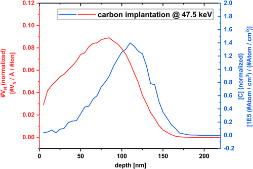
Carbon ions were homogeneously implanted into 18 × 18 mm2 samples by scanning the ion beam across the sample. For all implantation experiments, the samples were tilted by 7° with respect to the incident ion beam to avoid channeling. Three samples with varying carbon fluences of 8.1 × 10¹⁴, 8.1 × 10¹⁵, and 4.05 × 1016 cm−2 were prepared. Based on our simulation results depicted in Figure 1, this leads to peak carbon concentrations of ≈1.1 × 1020 cm−3 (sample A), ≈1.1 × 1021 cm−3 (sample B), and ≈5.7 × 1021 cm−3 (sample C). This sums up to [O] > [C] for sample A, [O] < [C] for sample B, and [O] << [C] for sample C, respectively. A conclusive discussion on the oxygen concentration is given in the next section. Further AlN samples were implanted with boron and neon as references. More details about the experimental design and parameters are published in our previous work.[ 19 ]
The HTA process was carried out inside a cold-wall furnace in N2 atmosphere at ambient pressure. All components inside the furnace consisted of porous Al2O3 (thermal isolation), sintered Al2O3 (tube, sample-holder), AlN (oxygen getter), and molybdenum (heater). This way, annealing took place in N2 atmosphere with negligible supply of oxygen from the gas phase. The AlN samples were annealed in face-to-face configuration to suppress thermal decomposition, as introduced by Miyake et al. in 2016 for AlN.[ 18, 29 ] This technique is also known as proximity cap annealing from other material systems.[ 30 ] After loading, the furnace was pump-purged between 50 mbar and ambient pressure three times with pure N2. After reaching 200 °C, the atmosphere was changed additionally twice to reduce moisture content. Subsequently, the temperature was set to 1,700 °C with a maximum heating rate of 8 K min−1 and dwell time of 3 h after reaching the set temperature, while purging the reactor with 5 slm of N2. After 3 h of dwell time, the heater was turned off and the samples cooled passively.
CL spectroscopy was carried out inside a Tescan Mira 3 GMH field emission scanning electron microscope (SEM). The microscope was equipped with a Gatan MonoCL4 system with a parabolic mirror for light collection and an Andor DV420-BV charge-coupled device (CCD) for the acquisition of emission spectra. Using an entrance slit width of 200 μm, the 300 L mm−1 grating inside the monochromator provides a spectral resolution of ≈2 nm on the CCD. To access a broad spectral range from 1.75 to 3.75 eV, but at the same time ensuring a high spectral resolution, the spectra shown in this work were composed of two single spectra leading to discontinuities at around 3 eV. If not specified differently, spectra of the carbon-implanted samples were measured using a beam current of ≈1.4 nA, acceleration voltage of 5 kV, and an integration time of 5 s. For the beam current-dependent measurements, an integration time of 10 s and a slit width of 500 μm were used to obtain a better signal-to-noise ratio for low currents. During the measurements, the samples were placed on a liquid nitrogen cryo-stage. The stage allows for measurement temperatures between 83 and 373 K by cooling or heating the sample holder, respectively.
In addition, time-resolved CL spectroscopy (TRCL) at cryogenic temperatures was performed in a Thermo Fisher Quattro S field emission SEM equipped with a Delmic Sparc cathodoluminescence system. Temporal resolution was achieved with an ultrafast beam blanking unit that was synchronized with a Hamamatsu StreakScope S20 streak camera mounted to the CL detection system. The measurement was performed at 20 K, which was ensured by mounting the sample onto a CryoVac KONTI helium flow cryostat that can reach sample temperatures in the range of 10–300 K. Analogously to the other CL experiments, the acceleration voltage was set to 5 kV. Moreover, a relatively large beam current of about 10 nA, a repetition rate of 5 MHz, and a long integration time of 10 min were used to ensure a reasonable signal-to-noise ratio.
3 Results and Discussions
To investigate the influence of carbon doping on the defect luminescence of HTA AlN, low-temperature CL measurements were carried out, as described in the Experimental Section. The luminescence spectra of nonimplanted HTA AlN in general consist of a broad defect band at a wavelength of 450–350 nm in the blue to UV-A range that has been ascribed to oxygen impurities forming complexes with V Al (i.e., one vacancy decorated with different amounts of oxygen atoms (VAl-nON) m−), as discussed by Kai et al.[ 31 ] and shown in Figure 2a. The origin is oxygen diffusion from the Al2O3 substrate during HT annealing.[ 24, 25 ] This feature is not only visible for HTA AlN but also observed for above bandgap excitation of low-[C], high-[O] PVT-grown AlN on tungsten substrates.[ 11 ] Thus, it seems to be a general feature of high-[O] AlN. This broad defect band, which will be abbreviated in the following with “B/UVA,” appears in all annealed samples, with or without ion implantation as also shown in Figure 2a. Hereafter, the B/UVA emission related to (VAl-nON) m− in AlN will not be discussed further, as investigations of this band are published elsewhere, for example, by Kai et al.[ 31 ]
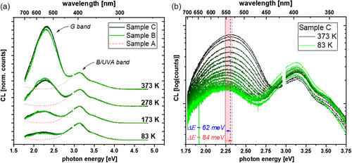
Due to a low CL intensity of the carbon-implanted and annealed samples, high-excitation currents and long integration times had to be used. Carbon doping seems to substantially increase recombination via a nonradiative channel, which is consistent with the incorporation of deep defects into AlN. According to the Shockley–Read–Hall (SRH) theory and under the assumption of a constant capture cross-section, the SRH model predicts stronger nonradiative recombination for traps that are close to the middle of the bandgap.[ 7, 8, 13 ] In the case of neon and boron implantation, HTA leads to recovery of the crystal without measurable energetic states inside the bandgap.[ 19 ] Thus, only the oxygen-complex-related (and therefore HTA-related) B/UVA band is measurable in the case of boron and neon implantation, but no further luminescence signal. Additionally, no decrease of CL intensity of the B/UVA band was measured compared to nonimplanted HTA AlN references, underlining the assumption that neon tends to diffuse out of the lattice during HTA and boron is incorporated into the Al-sublattice without introducing energetic states within the bandgap.[ 19 ]
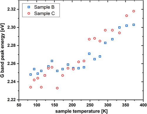
The CL spectra of the samples B and C (medium and high [C]) exhibit an additional broad signal in the green spectral range (denoted “G band” hereafter) centered at a photon energy of 2.25 eV at 83 K. Sample A does not show this broad green emission, cf. Figure 2a. This broad G band follows an inverse temperature quenching behavior, that is, an increasing intensity with rising temperature, as shown in Figure 2a,b. At the same time, the B/UVA band loses intensity relative to the G band. The described temperature behavior is shown in Figure 2a for the two highest carbon implant fluences, normalized to the CL count maximum of the B/UVA band to visualize the intensity change of the G band. Interestingly, the peak intensity ratios of the G and B/UVA bands between samples B and C are constant. Figure 2b underlines the inverse quenching with rising temperature and shows a blueshift of the G band with rising temperature of ≈84 meV. A similar blueshift is also observed for sample B. Figure 3 shows the peak energies of samples B and C plotted as a function of the measurement temperature. A detailed model for this shift will be discussed in the following section.
The G band of sample B shows a shoulder toward smaller energies in Figure 2a, which contains additional information. The nature of this transition is not entirely clear, even though a similar transition has already been attributed in the literature to free h + to A 2− transitions with (V Al –O N ) 1− as the ground state in axial configuration.[ 11, 32 ] The authors of these publications also describe the basal configuration of this defect complex, both theoretically via DFT and experimentally. The reported energy levels for both configurations correspond well to the two measured weak signals highlighted in Figure 4a. As the total defect luminescence intensity drops for increasing carbon fluence, the already weak h + to A 2− transition can only barely be distinguished from the background signal for sample C.
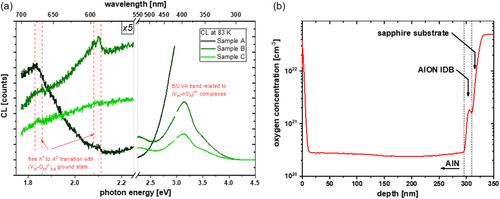
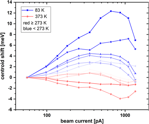
In addition to the inverse intensity quenching with temperature, the broad G band follows the already mentioned blueshift with rising temperature. A comparable blueshift can be measured for the B/UVA band even without any implantation and seems to be a general feature of high-[O] AlN, because the described behavior was observed by other groups as well: Schulz et al. reported a similar blueshift for defect bands in the blue spectral range.[ 33 ] In a previous publication, Lamprecht et al. related a broad band with a comparable blueshift—as measured for the G band in our work—at rising temperatures to a DAP between a shallow donor and an acceptor (they suggested a carbon-related defect, which fits also to our experimental design and our results).[ 13 ] Lamprecht et al. concluded that the involved donor species might be silicon in its D 0 ground state or DX − configuration. They based their conclusion on PL and PLE measurements, as well as calculations. In another publication, Lamprecht et al. reported about a second band that may be attributed to a transition from a shallow oxygen donor state at slightly lower energies, centered around 2.05 eV, to a similar acceptor.[ 14 ] However, all their measurements were performed on AlN bulk materials with different carbon, oxygen, and silicon concentrations compared to our samples, making the direct comparison of transition energies difficult due to the fact that transition energies of DA pairs depend on the involved impurity concentrations. The amount of oxygen in our HTA AlN is governed by diffusion from the sapphire substrate during HT annealing and can reach concentrations in the 3 × 1020 cm−3 range, as shown in the SIMS measurement in Figure 4b. Cancellara et al. measured [O] concentrations even reaching 6 × 1020 cm−3.[ 24 ] Since the emission wavelength of a DAP strongly depends on the Coulomb interaction between D + and A − after the charge transfer between D 0 and A 0 involved in the recombination process and hence their distance, DAP emission is blue-shifted for higher concentrations and broadened if the distance has a gradient over the layer thickness.[ 34-36 ] This is consistent with the broad appearance of the G band, as the carbon concentration will not be constant throughout the layer after implantation and HTA, thus leading to a broadening. A second reason for the width of the signal might be a high Huang–Rhys factor, thus a high number of involved phonons per recombination event (i.e., strong electron–phonon coupling). Furthermore, the G band does not only show a similar behavior with temperature compared to the one described by Lamprecht et al. but also reveals a DAP-specific blueshift of the emission band centroid depending on the excitation current I b at low temperatures and a stable emission maximum or small redshift for the same beam current series at higher temperatures, further supporting this model (cf. Figure 5 , measured at sample C). Higher temperatures lead to ionization of donors, and successively to a saturation of the blueshift that is measurable at low temperatures. The behavior changes approximately around 273 K from a strong blueshift to a slightly redshifted centroid. High excitation current densities are also supposed to locally heat the sample, thus leading to saturation of the blueshift, explaining the negative centroid shift at the highest beam currents. Screening effects due to strong excitation can also play a role in the redshifted centroid.
To corroborate our interpretation of the G band being DA-related, TRCL measurements were used to determine the lifetimes of the involved transitions in the G band. In the case of a DAP transition, the lifetimes at different wavelengths should shift, that is, have a lower value for the high-energy components of the G band, as such transitions are caused by DA pairs with smaller distance. The mean lifetime of a DAP depends on the overlap between the wave functions of the donor and acceptor, respectively.[ 37, 38 ] If A 0 and D 0 are spatially close to each other, the lifetime is short. At the same time, the Coulomb term has the highest values for a nearby DAP.[ 34-36 ] Consequently, a monotonically decreasing lifetime with emission energy is another fingerprint of a DAP transition. Figure 6a shows measured transients (dots) and fits (lines)—according to the fitting procedure described by Spende et al.[ 39 ]—with a 20 nm step width and a transient integration window of 5 nm. The decay times extracted from the fit are plotted in Figure 6b, revealing a monotonically decreasing lifetime from 490 to 590 nm. The extracted decay times are plotted within the spectrum of the G band for better visualization. To avoid crosstalk between the B/UVA and G bands and to achieve a good signal-to-noise ratio, transients were fitted in a wavelength range representing the FWHM of the G band.
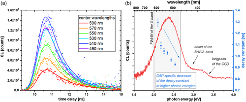
Using ε r = 8.39 as the geometric mean for ε r in AlN, the Coulomb term amounts to about 185 meV.[ 40 ] One has to keep in mind that this value surely varies over the layer thickness in the examined samples, as implantation profiles have a Pearson IV shape and are not constant over the layers’ depth.[ 41 ] According to the literature, as oxygen is expected to be the deep donor-type impurity involved in the transition, a value of E d = 340 meV for the ON donor can be assumed.[ 42 ] We are aware of the favored relaxation of oxygen into a self-compensating DX − state. Nonetheless, following the model of self-compensation, an equal amount of oxygen atoms should be in its D + and DX − configuration. During the experiment in a scanning electron microscope, one can expect the capture of generated electrons and thus formation of a neutral D 0 state which can take part in a DAP transition.
To calculate the energetic position of the acceptor E a, we are using Equation ( 1 ). Using published low-temperature values of the bandgap energy E g (6.089 eV at 12 K) and published Varshni parameters of AlN, one can calculate E g (83 K) for bulk AlN to be 6.081 eV.[ 43, 44 ] Since HTA AlN is compressively strained, we correct the bulk values of E g with published deformation potentials of AlN.[ 45 ] In spite of the differing expansion coefficients of AlN and sapphire and their influence on the actual strain level of the AlN, the temperature dependence due to the deformation potentials will be neglected. Thus, the only considered temperature dependence is the narrowing described by Varshni. Using the measured strain in the annealed layers via HRXRD of our samples (εxx = εyy = −0.00304 and εzz = 0.00186) as an input, the shift ΔE g of the bandgap energy E g as it follows from the used deformation potentials at room temperature can be simulated with Nextnano++ to around +25 meV, thus E g = 6.104 eV.[ 46 ] Therefore, Equation (1) yields E a = 3.70 eV, which fits excellently with the energy E a = 3.69 eV of the acceptor described by Lamprecht et al., which they assign as most likely carbon related, also agreeing to our experimental design.[ 13 ] Here, we want to highlight that E a is not necessarily the ionization energy of the acceptor, but rather an apparent ionization energy, as Equation (1) is classical and excludes quantization of vibrational states. In reality, a strong electron–phonon coupling leads to a strong Franck–Condon shift in the acceptor A − state, thus, the electron does not recombine into the vibrational ground state of the acceptor. Therefore, the Franck–Condon shift at the acceptor state is the difference between the real ionization energy and the apparent ionization energy E a = 3.70 eV, which we calculated above. A similar difference in measured and calculated ionization energies is known from the yellow luminescence in GaN, as discussed by Alkauskas et al. in their comprehensive review on defects in semiconductors.[ 15 ]
As the classical models used for DAP (Equation (1)) and free electron (Equation (3)) transitions fit excellently to our measurements and the calculated apparent ionization energy E a is in accordance with the results of Lamprecht et al., we want to repeat our assignment to oxygen (ON) and carbon (most likely CN) as the involved donors and acceptors, respectively, in the DAP transition.[ 13 ] The calculated transitions of CN in the literature and thus, ionization energy of this acceptor, deviate strongly from the herein published apparent ionization energy of E a = 3.70 eV. As we do not know the strength of the electron–phonon coupling and thus do not know the Franck–Condon shift at the acceptor, we cannot estimate the real ionization energy. Therefore, the involved acceptor may also be carbon-related, instead of carbon itself, that is, formed due to compensation effects during annealing or an acceptor-like complex formed of carbon and possibly oxygen, as both occur in high concentrations in our samples. Unfortunately, there are no theoretical studies that discuss acceptor-like complexes of carbon except the so-called carbon pair and tricarbon defects, which both are almost exclusively known from growth in the m-direction.[ 47, 48 ] Likewise, Lamprecht et al. also reviewed their results in a later publication. They found some contradictions regarding the acceptor attribution in their first and second publication[ 13, 14 ]: Results from DFT calculations of the acceptor ionization energy tend to prefer VAl or VAl-nON complexes instead of for example CN as the involved acceptor in the observed DAPs.[ 49 ] Finally, based on our experimental design, VAl-related complexes cannot explain the absence of the G band in sample A or nonimplanted reference samples. The high concentration of carbon should even suppress the formation of additional acceptor-type defects, relatively to sample A or nonimplanted HTA AlN. These results need to be debated in the future, supported by theoretical considerations.
Based on these measurements, we constructed a preliminary configuration diagram for high, intermediate, and low temperatures. The configuration has to explain the following main effects: a) Inverse quenching of the CL intensity with rising sample temperature. b) Blueshift of the G band emission with rising sample temperature.
The model is shown in Figure 7 . Note that the diagrams are purely qualitative, thus the shifts, slopes, and distances are not reflecting reality. Due to the strong electron–phonon coupling, indicated by the broad appearance of the G band, most values in the diagram are hardly accessible with our experimental setup. We assumed a temperature dependence for ΔQ = Q A,- − Q D,0 that leads to the respective minima of the parabolic potentials approaching each other if the temperature is increased. Some similar behavior was suggested by Ghosh et al. to explain their results.[ 50 ]
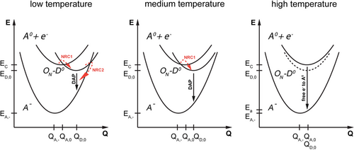
The relative location of the parabolic potentials at low temperature leads to two efficient nonradiative pathways for electrons excited into the conduction band at low temperatures. The first nonradiative capture (NRC1) between electrons in the conduction band (A 0 + e − ) and the ON -D 0 state leads to quenching of the free electron-to-acceptor transition. Therefore, the DAP is the dominating radiative recombination process at low temperature. The second nonradiative capture (NRC2) may explain the small CL intensity at low temperatures, thus, the inverse intensity quenching with rising temperature. By successively increasing the temperature, the barrier heights of NRC1 (after surpassing the minimum of the (A 0 + e − ) state) and NRC2 rise. Thus, a continuous change between the dominating DAP character at low temperature to a dominating (e − , A 0) character for increasing temperature can be explained. At the highest temperatures, ΔQ approaches the smallest values, which lead to disappearing interceptions (i.e., nonradiative pathways) or extremely high barriers between the potentials and thus no efficient feeding of the ON -D 0 state from the conduction band. The apparent ionization energy calculated with Equation (1-2)–(3) is also shown in the model in Figure 7 in the case of the free electron to acceptor transition.
4 Conclusions
Based on our results and the experimental design, we tentatively assign the involved acceptor in the measured DAP transition to be carbon related, or even CN. Compared with the latest considerations on DAPs in AlN, there are still inconsistencies between the up to now published results in the literature. Our results indicate that HTA AlN exhibits a donor (most likely ON) that very efficiently captures electrons from the conduction band at low temperature. This might also explain why AlN crystals that contain large impurity concentrations typically do not show band edge luminescence. Due to a disappearing nonradiative recombination path with increasing temperature, the defect luminescence of excessively oxygen-doped AlN shows a blueshift. In the case of the G band and based on our experimental design, this leads to a continuous change from a DAP transition between ON -D 0 and a carbon-related acceptor to a free electron-to-acceptor transition with most likely CN as the involved acceptor. Finally, we were able to confirm that the previously presented interpretation of measured DAP transitions in AlN also holds true for completely different impurity levels, yielding strikingly consistent results for the presumed acceptor energy level, whose origin is still open to be discussed. To undoubtedly identify the nature of this frequently addressed acceptor, more experiments and theoretical considerations are needed. These results indicate that the broad defect landscape of AlN is far from fully understood.
Acknowledgements
The authors also thank Patrick Hoffmann for his technical assistance on the implantations. This work was funded by Deutsche Forschungsgemeinschaft (DFG) in the framework of the SPP 2312 (Energieeffiziente Leistungselektronik “GaNius”), Project No. 462737320 (Aluminium Nitrid für die vertikale Leistungselektronik) and also in the framework of Germany's Excellence Strategy—EXC-2123 QuantumFrontiers—390837967. The authors also gratefully acknowledge the support of the Braunschweig International Graduate School of Metrology B-IGSM and the DFG Research Training Group 1952 Metrology for Complex Nanosystems.
Open Access funding enabled and organized by Projekt DEAL.
Conflict of Interest
The authors declare no conflict of interest.
Author Contributions
L.P. performed the annealing experiments, the simulations, major part of the CL measurements, processing of the data, and took active part in the writing of this article. H.S. performed parts of the CL measurements and supervised the TRCL measurements. S.W. performed the TRCL measurements. C.M. performed the HRXRD measurements. C.R. designed the ion implantation experiments. T.V. gave major advice on the CL data interpretation. A.W. acquired the funding for this project and supervised this research. All authors contributed to the discussion and writing of the article.
Open Research
Data Availability Statement
The data that support the findings of this study are available from the corresponding author upon reasonable request.


