Journal list menu


Following the established tradition in the pss journal family since 1999, pss (a) and pss (b) have once again published contributions based on workshop presentations in a twin special issue.
Export Citations
Download PDFs
Table of Contents
Electrical Characteristics of Gated Anode Diodes Based on Normally Off Recessed-Gate GaN High-Electron-Mobility Transistors for Rectenna Applications
- First Published: 03 March 2023
GaN high-electron-mobility transistor (HEMT)-based gated-anode diodes (GADs) for 5.8 GHz high-power rectenna application are proposed. Using HEMTs with a recessed gate structure, the GAD significantly improves maximum anode forward current and reverse breakdown voltage simultaneously. Rectifying performance simulated with SPICE model shows that the GAD is a promising device for high-power rectenna at 5.8 GHz.
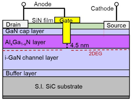
Si-Doping Effects in AlGaN Channel Layer on Performance of N-Polar AlGaN/AlN FETs
- First Published: 15 July 2023
AlN substrate offers various advantages, such as high breakdown voltage and high-temperature operation. Herein, a N-polar AlGaN/AlN-heterostructured field-effect transistor (FET) with static FET characteristics is successfully fabricated. However, the drain current density, IDS, remains significantly small. This study aims to improve IDS by doping Si in the topmost AlGaN channel layer under various conditions.
Comparative Performance Evaluation for 1.2–10kV Conventional and Superjunction GaN Current Aperture Vertical Electron Transistors
- First Published: 13 June 2023
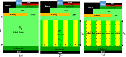
The performance potentials and limits for GaN current aperture vertical electron transistors with conventional, doped, and natural polarization (PSJ) superjunction drift layers at 1.2–10 kV BV ratings are quantitively compared by extracting their static and dynamic performance parameters using technology computer-aided design simulation. PSJ offers the best performance with at least 22% and 80% at 1.2 and 10 kV respectively.
Development of High-Reflectivity and Antireflection Dielectric Multilayer Mirrors for AlGaN-Based Ultraviolet-B Laser Diodes and their Device Applications
- First Published: 28 May 2023

Fabrication techniques for high-reflectivity (HR) and antireflection (AR) dielectric multilayer mirrors for AlGaN-based ultraviolet-B (UV-B) laser diodes are developed. By mounting those mirrors on both edges of the device, the improvement of device performance is confirmed, such as increased light output and slope efficiency.
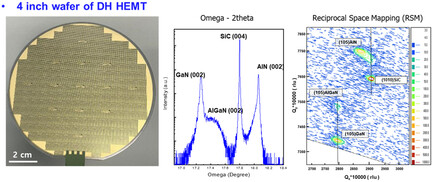
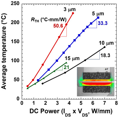
Electrothermal Performance of AlGaN/GaN Lateral Transistors with >10 μm Thick GaN Buffer on 200 mm Diameter-Engineered Substrates
- First Published: 03 May 2023
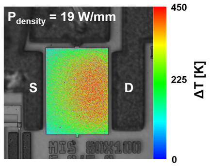
AlGaN/GaN lateral transistors fabricated with >10 μm thick buffers on 200 mm diameter-engineered substrates are demonstrated. The engineered substrates result in minimal residual stress in the GaN buffer while the fabricated transistors display both electrical and thermal performance competitive with other substrate technologies such as Si. A pathway for large-scale production of high-yield GaN devices is presented.
Metal–Organic Chemical Vapor Deposition-Grown AlScN for Microelectromechanical-Based Acoustic Filter Applications
- First Published: 12 June 2023
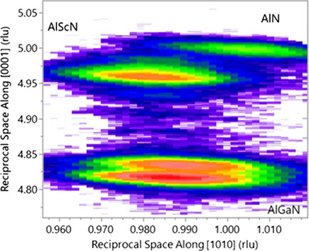
Piezoelectric AlScN single-crystal films deposited by metal–organic chemical vapor deposition are used for the first time in the fabrication of bulk acoustic wave filters. The effects of growth conditions are discussed and novel structures are produced to manage internal stresses and preserve planar surface morphology.
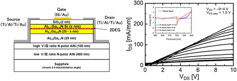
Investigation of Electrical Properties of N-Polar AlGaN/AlN Heterostructure Field-Effect Transistors
- First Published: 16 May 2023

Herein, N-polar Al0.1Ga0.9 N/Al0.9Ga0.1 N/AlN field-effect transistor (FET) is fabricated using metal–organic vapor-phase epitaxy, and the static FET operation is confirmed to exhibit an n-channel and pinch-off.
Power Performance of AlGaN/GaN High-Electron-Mobility Transistors with AlN Buffer on SiC Substrate at 3.5 GHz
- First Published: 20 April 2023
Herein, the power performance of an AlGaN/GaN high-electron-mobility transistor (HEMT) with AlN buffer on SiC substrate, grown by high-temperature metal–organic chemical vapor deposition, is presented. The fabricated devices are examined and show positive characteristics, such as low slump ratio and breakdown voltage. The potential of using an AlN buffer HEMT is demonstrated by the results for use in high-power radio-frequency devices of the future.
Effect of GaN/AlGaN Buffer Thickness on the Electrothermal Performance of AlGaN/GaN High Electron Mobility Transistors on Engineered Substrates
- First Published: 20 April 2023
AlGaN/GaN high electron mobility transistors (HEMTs) on engineered substrates are grown with different GaN/AlGaN buffer layer thickness and evaluated via atomic force microscopy, high-resolution X-ray diffraction, Raman spectroscopy, and steady-state thermoreflectance. Fabricated HEMTs are evaluated via DC and pulsed electrical techniques and thermoreflectance imaging. It is reported that these HEMTs exhibit high GaN quality, low stress, low current collapse, and low thermal resistance.
Fabrication of Low On-Resistance and Normally Off AlGaN/GaN Metal Oxide Semiconductor Heterojunction Field-Effect Transistors with AlGaN Back Barrier by the Selective Area Regrowth Technique
- First Published: 25 April 2023

Cross-sectional transmission electron microscope (TEM) images of the recessed-gate structure on a thin AlGaN/GaN channel metal oxide semiconductor heterojunction field-effect transistor fabricated by selective area regrowth. The thin AlGaN/GaN channel with an AlGaN back barrier and the regrown AlGaN/GaN high electron mobility transistor structure provides low on-resistance and normally off operation.
Bright Emission at Reverse Bias After Trailing Edge of Driving Pulse in Wide InGaN Quantum Wells
- First Published: 21 April 2023
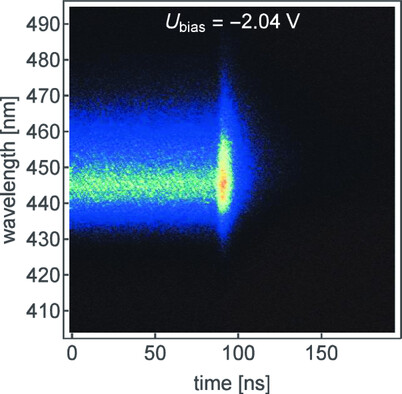
Laser diodes with different InGaN quantum well thicknesses up to 25 nm are analyzed. Efficient screening of the piezoelectric field and excited-state operation are reported. The time-dependent behavior below threshold gives insights about the quantum well tilt and the wave function overlap. A sharp intensity increase and wavelength shift are observed at the end of the pulse.
Suppression of Reverse Leakage in Enhancement-Mode GaN High-Electron-Mobility Transistor by Extended PGaN Technology
- First Published: 18 April 2023

An extended PGaN gate structure that can reduce the peak electric field is proposed and successfully adopted on a Schottky PGaN enhancement-mode GaN high-electron-mobility transistor platform. The device features a saturation current of 256 mA mm−1, a threshold voltage of +1.8 V, and an ON-resistance of 19.781 Ω mm.
Performance of Ultraviolet-B Laser Diodes on AlGaN Templates Prepared Using Different Fabrication Methods
- First Published: 03 March 2023
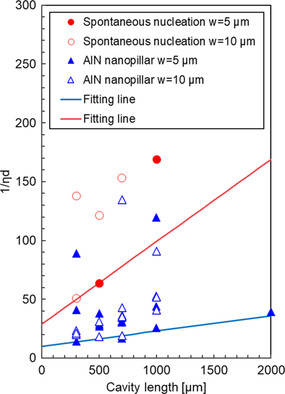
AlGaN templates are fabricated using the spontaneous nucleation and AlN nanopillar methods, and ultraviolet-B (UV-B) laser diodes (LDs) with the same structure are fabricated on them. Herein, three and six times higher values for Sd and Ppeak are confirmed, respectively, using templates fabricated using the AlN nanopillar method. The method of AlN nanopillars is realized by high-performance UV-B LDs.
Performance and Degradation of Commercial Ultraviolet-C Light-Emitting Diodes for Disinfection Purposes
- First Published: 13 April 2023

The reliability of ultraviolet-C (UV-C) light-emitting diodes (LEDs) is crucial for next-generation disinfection systems. Herein, the electrical, optical, and spectral properties of UV-C LEDs with an emission peak of 275 nm during their lifetime are analyzed. The analysis allows to determine the optimal balance between performance, reliability, and costs in a solid-state disinfection system.
Recent Progress of E-mode Gallium Nitride Metal–Insulator–Semiconductor -High Electron Mobility Transistors with Hybrid Ferroelectric Charge Trap Gate (FEG-HEMT) for Power Switching Applications
- First Published: 30 March 2023

The high-performance ferroelectric charge storage gate (FEG) gallium nitride high-electron-mobility transistors (HEMT) has gradually gained attention due to the concept being a useful tool to realize E-mode operations, which has been a focused topic in recent years for their potential applications. This article attempts to review the latest progress in this technology, including alternative improvements and device characteristics.
Realization of Low Dislocation Density AlN on Patterned Sapphire Substrate by Hydride Vapor-Phase Epitaxy for Deep Ultraviolet Light-Emitting Diodes
- First Published: 30 March 2023
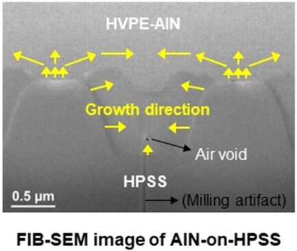
By introducing the hole-type patterned sapphire substrate (HPSS) with a properly designed pattern configuration as a substrate for AlN growth, threading dislocation density (TDD) is significantly lowered from 1.48 × 10⁹ to 4.38 × 108 cm−2. The TDs on the mesa zones generated at AlN/sapphire interface can be effectively suppressed by bending toward coalescence zone during the subsequent lateral overgrowth.
Electrical Behavior of Vertical Pt/Au Schottky Diodes on GaN Homoepitaxy
- First Published: 30 March 2023
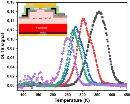
I–V characteristics investigation in the function of temperature shows barrier height inhomogeneities for vertical GaN Schottky diodes. These inhomogeneities are a common and crucial issue for power device application. Their potential origin (strain, doping variation, electrically active defects) is studied using Raman spectroscopy and deep-level transient spectroscopy.
Highly Sensitive Hydrogen Sulfide Sensor Based on GaN/GaInN Heterostructure
- First Published: 24 March 2023

GaInN heterostructure sensors are optimized primarily for hydrogen sulfide sensing. Thin GaN cap layer, thick GaInN quantum well (QW), and low-doping concentration with a gold functionalization layer are found to be better for sensitivity in the 10–100 parts per billion (ppb) range. Ammonia gas is also detected in the 5–10 ppm range.
Novel Codoping Moiety to Achieve Enhanced P-Type Doping in GaN by Ion Implantation
- First Published: 16 March 2023
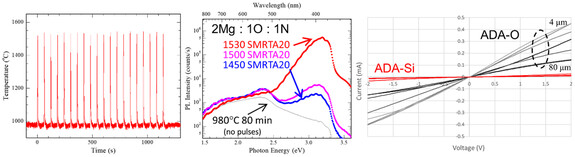
Codoping of gallium nitride for improved acceptor ionization has long been theorized; here we show significantly improved p-type doping of GaN with donor coimplantation for formation of low-activation energy complexes. Transmission line measurements, photoluminescence, and p-type hall exhibit vast improvement with additional oxygen donors compared to silicon having significant implications for device topologies requiring colocated dopants or utilizing n-polar material.
Sign up for email alerts
Tools
![]()
In 2022, the youngest family member physica status solidi (RRL) – Rapid Research Letters is turning 15 years. To celebrate this milestone, we present a new virtual collection with invited articles.
![]()
As we celebrate the 60th anniversary year of the physica status solidi family, click here to access our continuously updated collection of invited articles written by authors and partners of the pss journals.