Journal list menu

 Issue
Issuephysica status solidi (a): Volume 217, Issue 3
Special Issue:Compound Semiconductors
February 2020Guest Editor(s):
Export Citations
Download PDFs
Cover Picture
Molecular Beam Epitaxy of Transition Metal Nitrides for Superconducting Device Applications
- First Published: 06 February 2020

Superconductors
Integration of superconductors with semiconductors is required for high-performance electron devices in new quantum, sensing, and systems applications. In article number 1900675, D. Scott Katzer and co-workers report the fully epitaxial integration of III-N and GaN HEMT structures on superconducting transition metal nitrides. Image created by Robert Kurcoba using an atomic image provided by Ph.D. student Yimo Han and Professor David Muller at Cornell University.
Masthead
Back Cover
Revelation of Dislocations in β-Ga2O3 Substrates Grown by Edge-Defined Film-Fed Growth
- First Published: 06 February 2020

Chemical Etching
This figure is a schematic drawing of the experimental setup and principle of the synchrotron X-ray topography used for the observation of dislocations in β-Ga2O3 crystal. Two types of surface orientation of the samples are indicated in the crystal structure of β-Ga2O3 visualized by VESTA software. More details can be found in article number 1900630 by Yongzhao Yao and co-workers.
Editorials
Feature Articles
Molecular Beam Epitaxy of Transition Metal Nitrides for Superconducting Device Applications
- First Published: 12 October 2019

Molecular beam epitaxy is used to grow epitaxial III-N and GaN high electron mobility transistor (HEMT) structures directly integrated with epitaxial transition metal nitride materials. The growth conditions used, and the physical and electronic properties of the films are reported, including the first epitaxial integration of GaN HEMT transistors with an epitaxial superconducting load.
Indium Phosphide Membrane Nanophotonic Integrated Circuits on Silicon
- First Published: 03 December 2019
Indium phosphide (InP) membrane photonics on silicon (IMOS) combines the high-density nanophotonic circuitries and the high-efficiency direct-bandgap optoelectronics in a single micrometer-thick membrane layer. It enables strong light-matter interaction in the membrane, leading to a range of performance enhancements. Integrating this InP membrane on electronics wafer will enable revolutionary cointegration and convergence of photonics and electronics.
Original Papers
Revelation of Dislocations in β-Ga2O3 Substrates Grown by Edge-Defined Film-Fed Growth
- First Published: 28 September 2019

Chemical etching and synchrotron X-ray topography (XRT) are used to evaluate crystallographic defects in β-Ga2O3 substrates grown by edge-defined film-fed growth. Dislocations and stacking faults are revealed by etching in a eutectic molten KOH + NaOH solution at 200 °C for 2 min. Correlation between the positions of the etch features and defects are confirmed by XRT.
Effects of Bi Irradiation on the Molecular Beam Epitaxy Growth of GaSb on Ge (111) Vicinal Substrates
- First Published: 13 July 2019

The molecular beam epitaxy growth of GaSb on Ge (111) vicinal substrates is performed with Bi irradiation. The effects of the Bi irradiation on the surface morphology and on the crystallinity are investigated using atomic force microscopy and X-ray diffraction, respectively. It is shown that Bi works as a surfactant, which suppresses the generation of rotational twins in the GaSb layer.
Vertical β-Ga2O3 Schottky Barrier Diodes with Enhanced Breakdown Voltage and High Switching Performance
- First Published: 31 August 2019

Herein, vertical β-Ga2O3 Schottky barrier diodes (SBDs) with an ion-implantation-based planar edge termination structure are developed and their switching performance is also investigated. The devices exhibit greatly enhanced reverse blocking characteristics and fast switching performance. The results indicate a great promise of vertical β-Ga2O3 SBDs for high-voltage fast switching applications.
Fabrication of CH3NH3PbBr3-Based Perovskite Single-Crystal Arrays by Spin-Coating Method Using Hydrophobic Patterned Substrate
- First Published: 06 December 2019
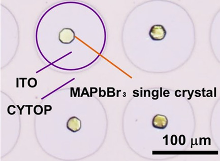
A simple and low-cost fabrication technique is proposed for CH3NH3PbBr3-based perovskite single-crystal arrays by combining spin coating and a hydrophobic/hydrophilic patterned substrate. By optimizing the substrate surface treatment, blending ratio of precursor solution, and spinning condition, the precursor solution is uniformly aligned on a hydrophobic pattern area and perovskite single crystals are precipitated at the center of the pattern area.
Growth of InGaAs Solar Cells on InP(001) Miscut Substrates Using Solid-Source Molecular Beam Epitaxy
- First Published: 31 August 2019
Herein, lattice-matched InGaAs solar cells grown on InP substrates via solid-source molecular beam epitaxy are investigated. It is found that the growth at 490 °C on InP(001) miscut 2° toward (111)A promotes step-flow growth, resulting in less nonradiative recombination. As a result, the lowest bandgap−open-circuit voltage deficit of 369 mV is obtained.
Highdetectivity AlInSb Midinfrared Photodiode Sensors with Dislocation Filter Layers for Gas Sensing
- First Published: 12 October 2019

The photodiode for the methane gas sensor is fabricated in the AlInSb/GaAs system. Inserting optimized dislocation filter layers (DFLs) decreases the dislocation density in the active layer to 1.1 × 109cm−2. This improvement produces a normal incidence detectivity of 1.8 × 109 cm √Hz W−1 at 3.3 μm, which is more than twice the highest detectivity previously obtained for a photodiode without DFLs.
Improved Electron Transport Properties of Ga1–xInxSb Quantum Well Channel Using Strained-Al0.40In0.60Sb/Al1–yInySb Stepped Buffer
- First Published: 24 October 2019
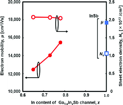
Unstrained Ga1–xInxSb quantum well (QW) channel using strained-Al0.40In0.60Sb/Al1–yInySb stepped buffer layer is investigated. The Ga1–xInxSb QW is lattice-matched to the Al1–yInySb lower buffer layer. The Te-δ-doped Al0.40In0.60Sb barrier layer is grown on the Ga1–xInxSb QW. Sheet electron density (Ns) of Ga1–xInxSb QW is about twice that of InSb one. Thus, increasing Ns while keeping relatively high electron mobility is successful.
The Effect of Introducing Optical Blanking on GaN Epitaxy Using Pulsed Laser Deposition Technology
- First Published: 13 August 2019

Ge-doped GaN is grown by pulsed laser deposition with pico-second laser. Incorporation of laser braking not only improves growth uniformity with a carrier density of 3.5 × 1020 cm−3 but also achieves to fabricate non-alloy ohmic. In addition, the laser blanking results in complete elimination of Ga droplet even at the growth temperature of 500 °C.
Evolution and Recovery of Electrical Property of Reactive Sputtered Al-Doped ZnO Transparent Electrode Exposed to Harsh Environment
- First Published: 19 October 2019
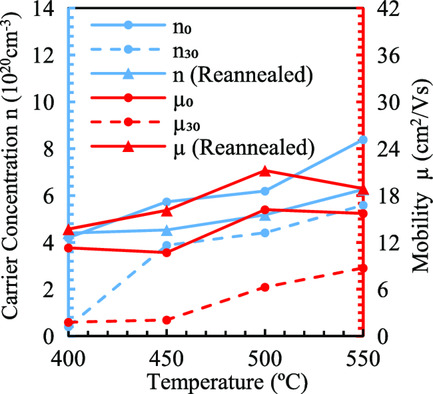
Degradation of electrical properties is observed for aluminum-doped zinc oxide (AZO) thin films exposed to a harsh environment. Recovery is achieved by reannealing the degraded AZO films in a hydrogen atmosphere at 400–550 °C. This indicates that the degradation mechanism involves chemical aspects such as diffusion of water molecules, which is reversible, rather than physical damage to the films.
Regional Bandgap Tailoring of 1550 nm-Band InAs Quantum Dot Intermixing by Controlling Ion Implantation Depth
- First Published: 09 November 2019
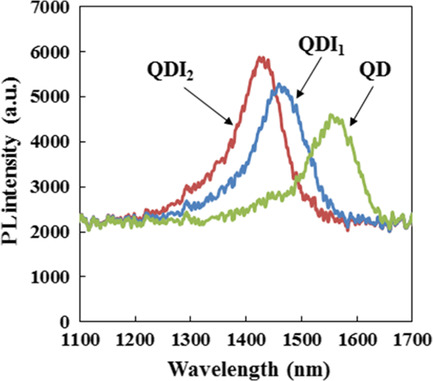
The regional control of bandgap energies using the highly stacked quantum dot (QD) on InP(311)B substrate changing ion implantation depths in the process of the quantum dot intermixing (QDI) technique is investigated. Controlled blue shifts of the photoluminescence (PL) spectra verify effectiveness of the regionally controlled QDI process for application to semiconductor photonic integrated circuits using 1550 nm-band QD.
Epitaxial Growth of High-Quality AlGaInAs-Based Active Structures on a Directly Bonded InP-SiO2/Si Substrate
- First Published: 27 November 2019
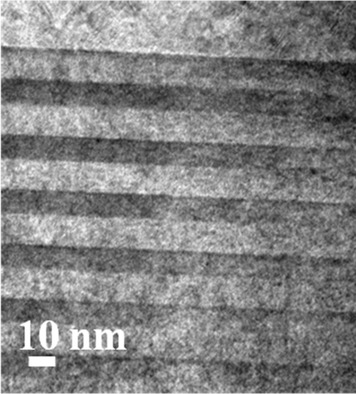
Epitaxial growth of AlGaInAs-based multiquantum wells heterostructure on a directly bonded InP-SiO2/Si substrate is evaluated. The thermal strain induced in the bonded membrane is assessed from in situ curvature measurement carried out during growth. Ex situ characterizations account for the high crystal quality of the structure compared to a reference grown on InP substrate.
Buried-Tunnel Junction Current Injection for InP-Based Nanomembrane Photonic Crystal Surface Emitting Lasers on Silicon
- First Published: 12 September 2019
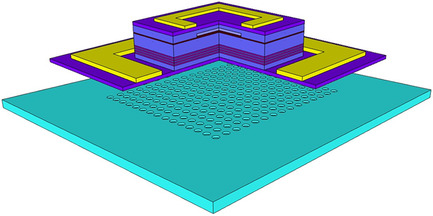
The design, fabrication, and performance of buried-tunnel junction (BTJ) current injection structures for InP/Si hybrid photonic crystal surface emitting lasers (PCSELs) are reported. Corresponding BTJ-light-emitting diodes on InP substrate show low series resistance and uniform carrier injection, whereas BTJ-PCSEL structures with similar current injection configuration fabricated on photonic-crystal silicon-on-insulator substrate using transfer print technology show significant linewidth narrowing at low current.
Top-Gated Polymer Light-Emitting Transistors Based on the Device Fabrication without Intermixing of Poly(methyl methacrylate) Gate Dielectric Formed from Fluorine-Based Orthogonal Solvent
- First Published: 24 September 2019

The fabrication process of a gate dielectric using poly(methyl methacrylate) (PMMA) solution in a fluorine-based solvent onto the active layers based on various semiconductors without intermixing can be applied to top-gated organic light-emitting transistors. For a device with Pt-tetraphenyltetrabenzoporphyrin [Pt(tpbp)] doped in poly(9,9-dioctylfluorene) (F8), a near-infrared emission from Pt(tpbp) and a relatively high external quantum efficiency of approximately 1% are achieved.
GaN-Based Monolithic Inverter Consisting of Enhancement- and Depletion-Mode MOSFETs by Si Ion Implantation
- First Published: 19 October 2019
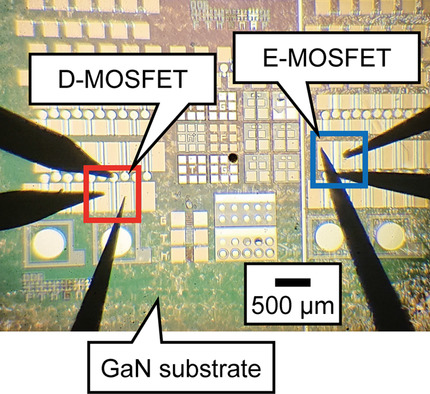
The successful operation of an enhancement/depletion (E/D)-type inverter consisting of n-channel enhancement- and depletion-mode MOSFETs (E-MOSFET and D-MOSFET) fabricated on a low Mg concentration p-GaN layer on GaN substrate with a maximum voltage gain 1.5 beyond unity is presented. Study of Si ion-implantation effects on GaN for GaN-based monolithic inverter is also reported.
Metalorganic Chemical Vapor Deposition of over 150-nm-Thick Quaternary AlGaInN Epitaxial Films near Alloy Composition Lattice-Matching to GaN on Sapphire and Their Structural and Optical Characterization
- First Published: 10 October 2019

Over 150-nm-thick AlGaInN films near alloy compositions lattice-matching to GaN on sapphire are grown by metalorganic chemical vapor deposition, and they showed relatively flat surfaces regardless of their lattice strains. Their crystal mosaicity probably depended on that of the underlying GaN films. Optical characterization results indicated that there is a certain degree of compositional fluctuation in the films.
Intersystem Crossing Rate in Thermally Activated Delayed Fluorescence Emitters
- First Published: 16 October 2019
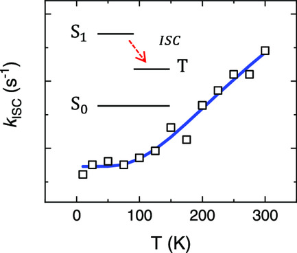
A method to determine the intersystem crossing rate (kISC) in thermally activated delayed fluorescence (TADF) emitters is reconsidered. Since the method widely used in the literature may cause errors at low temperatures, an alternative approach is devised. The kISC values determined with this approach for two TADF emitters from 10 to 300 K are also presented.
Organic Sensor Array Distributed in Flexible and Curved Surfaces
- First Published: 09 October 2019

A prototype of an artificial tactile sense of a soft robot finger which is expected to substitute sensitive human finger and to be engaged in high precision works is proposed. Curved surface consisting of thermally molded plastic film is effective because it has smooth shape that is realistic to the original 3D designed mold.
Direct Heteroepitaxy of Orientation-Patterned GaP on GaAs by Hydride Vapor Phase Epitaxy for Quasi-Phase-Matching Applications
- First Published: 06 October 2019
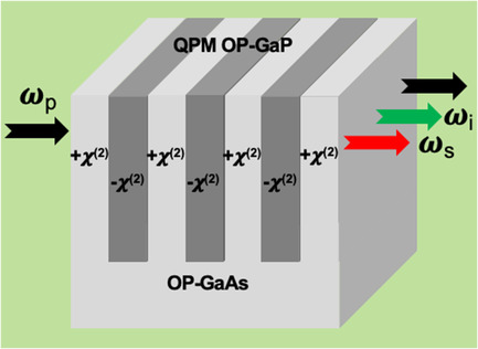
Quasi-phase-matched orientation-patterned GaP (OP-GaP) is a promising technology for mid-infrared and terahertz frequency generation. This work investigates the heteroepitaxy of OP-GaP on OP-GaAs template to exploit their complementary beneficial properties. By mitigating the adverse impact of lattice mismatching defects on the development of domain boundaries, OP-GaP with a high domain fidelity is obtained on OP-GaAs with a high growth rate.
Low-Temperature Selective Growth of Heavily Boron-Doped Germanium Source/Drain Layers for Advanced pMOS Devices
- First Published: 26 October 2019

The peculiarities of heavily boron-doped germanium, selectively grown at low temperature by means of a cyclic deposition and etch chemical vapor deposition process, are investigated through the analysis of the structural and electrical material properties. The experimental studies are supported by first principles simulations which are used to understand dopant deactivation mechanisms in the Ge:B system.
Hydride Vapor-Phase Epitaxy Reactor for Bulk GaN Growth
- First Published: 10 December 2019

Designing a hydride vapor-phase epitaxy reactor for bulk GaN growth is a challenging task where issues of chemical resistance, uniformity, repeatability, and long nonstop growth should be addressed. A quartz-free reactor with external precursor sources and a vacuum load-lock chamber is developed and tested in operation with more than a thousand growth processes performed.
Electrical Properties of Sn-Doped α-Ga2O3 Films on m-Plane Sapphire Substrates Grown by Mist Chemical Vapor Deposition
- First Published: 20 December 2019

Growth and electrical property of conductive Sn-doped α-Ga2O3 films on m-plane sapphire by mist chemical vapor deposition (mist-CVD) are exhibited. α-Ga2O3 films on m-plane sapphires with the thickness of 2 μm show mobility as high as 65 cm2 (V s)−1, which is much higher than previously reported value of 24 cm2 (V s)−1 in the films grown on c-plane sapphire.
Sign up for email alerts
Tools
![]()
In 2022, the youngest family member physica status solidi (RRL) – Rapid Research Letters is turning 15 years. To celebrate this milestone, we present a new virtual collection with invited articles.
![]()
As we celebrate the 60th anniversary year of the physica status solidi family, click here to access our continuously updated collection of invited articles written by authors and partners of the pss journals.