Journal list menu

 Issue
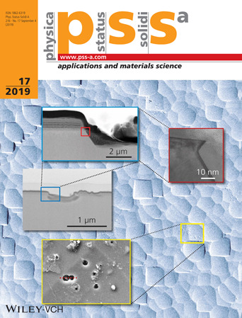
Issuephysica status solidi (a): Volume 216, Issue 17
Special Issue:Gettering and Defect Engineering in Semiconductor Technology
September 2019Guest Editor(s):
Export Citations
Download PDFs
Cover Picture
In Situ Observation of the Degradation in Multi-Crystalline Si Solar Cells by Electroluminescence
- First Published: 11 September 2019

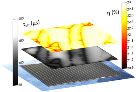
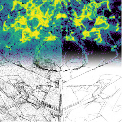
Comparison of microstructure (MS), initial electroluminescence (EL) and photoluminescence (PL) images with the strength of LETID effect (detected by EL) from the same location in mc-Si solar cell fabricated in PERC technology. Note the close correspondence of LETID effect with MS and PL and a much worse correlation between MS and EL. In the study, we used EL, PL methods together with capacitance-voltage (CV) and deep-level transient spectroscopy (DLTS) technique to get insight into the roots of LETID. More details can be found in article number 1800918 by Teimuraz Mchedlidze, Joerg Weber, and co-workers.
Inside Front Cover
Microstructural Analysis of Local Silicon Corrosion of Bifacial Solar Cells as Root Cause of Potential-Induced Degradation at the Rear Side
- First Published: 11 September 2019
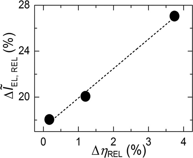
Industrial bifacial PERC solar cells show a new type of potential induced degradation (PID) at the rear side. After PID stress, cells exhibit power losses about 12 %rel. The origin of the losses is traced back to a local silicon corrosion, forming hole shaped damages within the passivation layers at the rear side. More details can be found in article number 1900334 by Kai Sporleder, Christian Hagendorf, and co-workers.
Masthead
Back Cover
Fundamental Characteristics of Cyanide-Related Multielement Molecular Ion-Implanted Epitaxial Si Wafers for High-Performance CMOS Image Sensors
- First Published: 11 September 2019
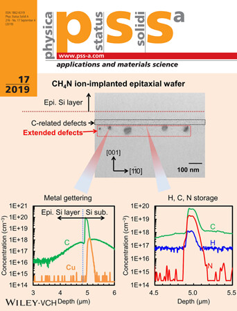
To improve the performance of CMOS image sensors, the authors currently develop a cyanide-related multielement molecular (CH4N) ion-implanted epitaxial Si wafer. The CH4N ion-implanted epitaxial Si wafer has two kinds of defects; C agglomeration defects and stacking faults. These defects contribute to high metal gettering capability and retention capability for H, C, and N. More details can be found in article number 1900172 by Akihiro Suzuki, Kazunari Kurita, and co-workers.
Editorials
Gettering and Defect Engineering in Semiconductor Technology (GADEST 2019)
- First Published: 11 September 2019
Feature Articles
Device Performance as a Metrology Tool to Detect Metals in Silicon
- First Published: 26 June 2019
Transition metals strongly impact the electrical device performance, i.e., carrier lifetime, leakage current, low-frequency noise, photocurrent, and solar cell efficiency. CMOS image sensors (CIS) and solar cells are also degraded by metal contamination. Density functional theory (DFT) ab initio calculations are frequently used to get a deeper physical insight in the defect structure. These different aspects are briefly reviewed.
Boron–Oxygen Complex Responsible for Light-Induced Degradation in Silicon Photovoltaic Cells: A New Insight into the Problem
- First Published: 02 July 2019
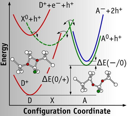
Experimental results on the electronic and dynamic properties of a defect consisting of a substitutional boron atom and an oxygen dimer (BsO2) in silicon are presented. It is shown that the BsO2 complex is a defect with negative-U properties, and it is responsible for persistent photoconductivity and light-induced degradation of efficiency of solar cells produced from Si:B+O crystals.
Limiting Defects in n-Type Multicrystalline Silicon Solar Cells
- First Published: 04 July 2019
This article reports on the characterization of defects limiting n-type multicrystalline silicon solar cells. Both defect identification and quantitative assessment of the defects' impact on cell performance are addressed. A higher tolerance against common metallic point defects is found. Material limitation becomes evident at decorated structural defects, such as dislocation clusters and grain boundaries.
Original Papers
Si Solar Cells
In Situ Observation of the Degradation in Multi-Crystalline Si Solar Cells by Electroluminescence
- First Published: 27 March 2019
Carrier-induced degradation in mc-Si silicon is investigated in situ using electroluminescence from the solar cells. The study is conducted at room and elevated temperatures and under various forward current conditions. The results are compared to the structure and J(V) characteristics of the cells.
Microstructural Analysis of Local Silicon Corrosion of Bifacial Solar Cells as Root Cause of Potential-Induced Degradation at the Rear Side
- First Published: 06 July 2019
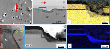
Bifacial passivated emitter and rear cells (PERC+) can suffer from a potential-induced degradation (PID) at the rear side. A microstructural analysis shows localized spots with increased carrier recombination as the origin of the power losses. A corrosion of the silicon bulk at the silicon/aluminium oxide interface is the root cause of the degradation.
Multielement Molecular Ion
Fundamental Characteristics of Cyanide-Related Multielement Molecular Ion-Implanted Epitaxial Si Wafers for High-Performance CMOS Image Sensors
- First Published: 29 May 2019
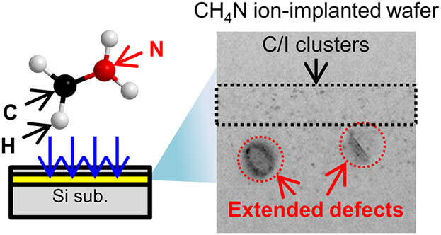
CH4N multielement molecularCH4N multielement molecular ion-implanted epitaxial Si wafer is a promising product for enhance the performance of CMOS image sensor.TheCH4N ion-implanted epitaxial wafer has high gettering capability for metals, hydrogen, carbon, and nitrogen. It is suggested that C-self interstitial agglomerations and extended stacking faults in the CH4N ion-implanted region contribute to the gettering capability for metals and light elements.
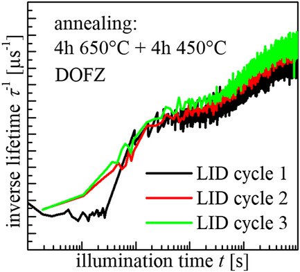
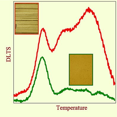
Location and Properties of Carrier Traps in mc-Si Solar Cells Subjected to Degradation at Elevated Temperatures
- First Published: 04 June 2019
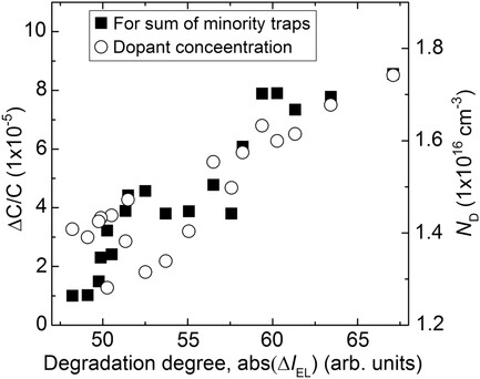
In mc-Si solar cells degraded at elevated temperatures under carrier injection (CeTID, LeTID), the degree of local degradation correlates with the local concentration of minority traps activated during the degradation, with local doping level and local density of structural defects.
Stacking Fault
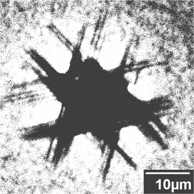
Annealing and LEEBI Effects on the Stacking Fault Expansion and Shrinking in 4H-SiC
- First Published: 29 May 2019

The expansion of SSFs due to e-beam irradiation is studied. The velocity of dislocations driving SSF expansion is independent of a distance from an imprint center and increases practically linear with beam current. The driving force for the expansion is mainly determined by the energy gain due to electron capture into SSF quantum wells associated.
Sonochemical Modification of SiGe Layers for Photovoltaic Applications
- First Published: 03 July 2019
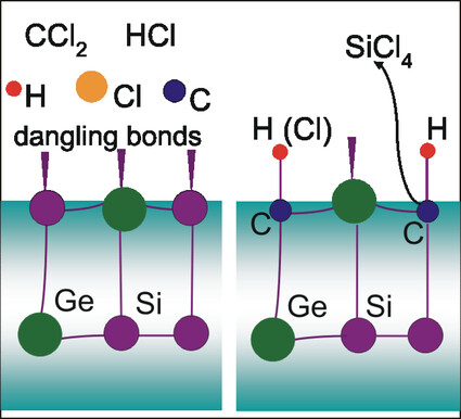
SiGe and a-Si/SiGe surfaces are sonochemically treated in chloroform (CHCl3) to improve the photovoltaic performance. The photovoltage magnitude and decay time can increase up to 50%. It is proposed that reactive Si dangling bonds revealed on the surfaces are saturated by the hydrocarbon species decomposed from CHCl3. This surface passivation can be promising for improving SiGe-based photovoltaic materials.
Dislocation Mobility
Estimations of Low Temperature Dislocation Mobility in GaN
- First Published: 28 May 2019
The activation energy of dislocation mobility in GaN is estimated from the measurements of traveling distances of dislocations gliding in pyramidal planes in the temperature range from 300 to 773 K. Its value is obtained to be equal to 650 ± 230 meV.
On a Novel Source Technology for Deep Aluminum Diffusion for Silicon Power Electronics
- First Published: 04 June 2019
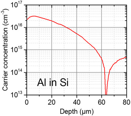
A low-cost technology is presented for the realization of high breakdown voltages in power electronics that allows the deep diffusion of aluminum from a physically deposited source. The approach requires only standard process steps that are already established in the manufacturing of silicon power devices. A full numerical analysis of the resulting profiles is provided.
Hydrocarbon Molecular Ions
Molecular and Atomic Hydrogen Diffusion Behavior by Reaction Kinetic Analysis in Projection Range of Hydrocarbon Molecular Ion for CMOS Image Sensors
- First Published: 28 May 2019
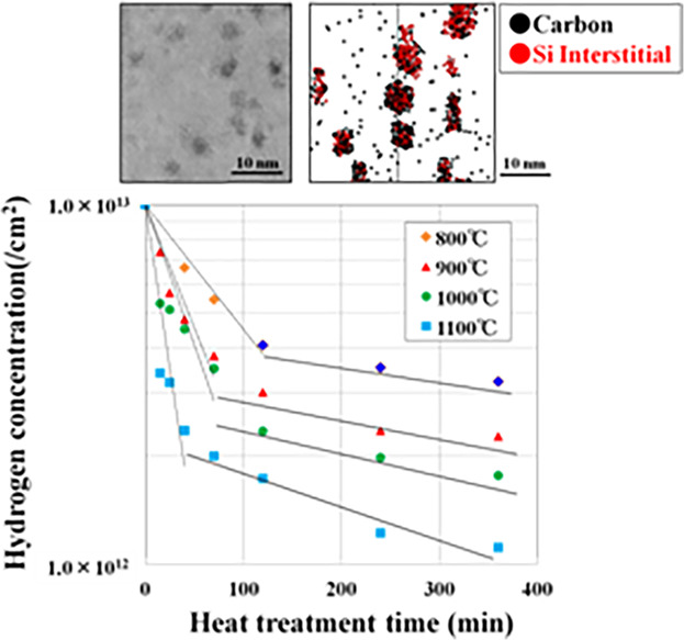
This paper presents two types of hydrogen diffusion behavior in the projection range of a hydrocarbon molecular ion for the CMOS image sensor. Two dissociation activation energies are determined by reaction kinetic analysis. The dissociation activation energy of 0.79 eV indicates molecular hydrogen diffusion, whereas that of 0.42 eV indicates atomic hydrogen diffusion.
Annealing of Pt-H Defects in High-Voltage Si p+/n− Diodes
- First Published: 04 June 2019
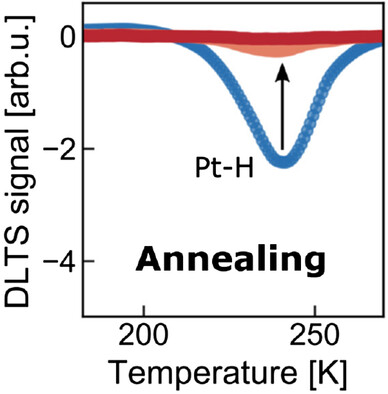
Silicon high voltage p+/n− diodes are intentionally doped with platinum for minority carrier lifetime adjustment. However, platinum–hydrogen (Pt–H) defects are formed during processing, which are degrading the reverse characteristics of these diodes. Therefore, the annealing of these defects is investigated via deep-level transient spectroscopy (DLTS) and modeled via a first-order dissociation reaction.
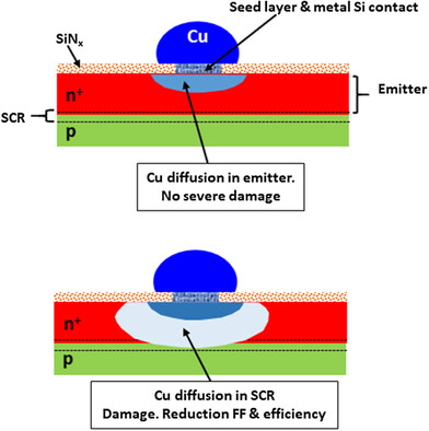
Gettering Mechanism of Copper in n-Type Silicon Wafers
- First Published: 17 June 2019
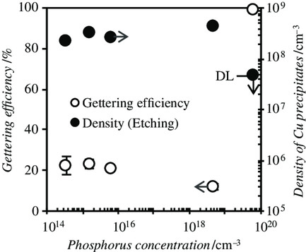
To reveal the gettering mechanism of copper, the dependence of gettering efficiency and copper precipitation on dopant concentration is investigated using n-type silicon wafers. Copper precipitates below a dopant concentration of 1019 cm−3, while no copper precipitates above 1019 cm−3 although strong gettering occurs, suggesting that the gettering mechanism changes from relaxation to segregation with increasing dopant concentration.
Fabrication of Medium Power Insulated Gate Bipolar Transistors Using 300 mm Magnetic Czochralski Silicon Wafers
- First Published: 14 June 2019
The use of 300 mm silicon wafers strongly increases the productivity of a manufacturing line for insulated gate bipolar transistors. However, 300 mm float-zone silicon is not available, so that the Czochralski material is required. For this, several critical issues have to be solved: crystal originated particles, the axial-doping variation along the crystal, and the minimization of the concentration of CIOIH complexes.
Impact of In Situ Annealing on the Deep Levels in Ni-Au/AlN/Si Metal–Insulator–Semiconductor Capacitors
- First Published: 05 July 2019
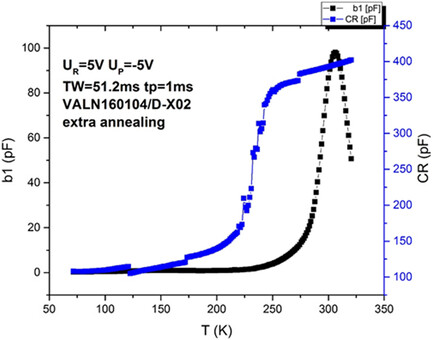
The impact of in situ annealing on the electrical properties of AlN/(111) p-type silicon metal–insulator–semiconductor (MIS) capacitors is studied by capacitance–voltage (C–V) and deep-level transient spectroscopy (DLTS). It is demonstrated that the in-diffusion of Al leads to an enhanced free hole concentration close to the interface and the presence of near mid-gap hole traps. The trap parameters are modified by the annealing treatment.
Dissociation and Formation Kinetics of Iron–Boron Pairs in Silicon after Phosphorus Implantation Gettering
- First Published: 25 July 2019
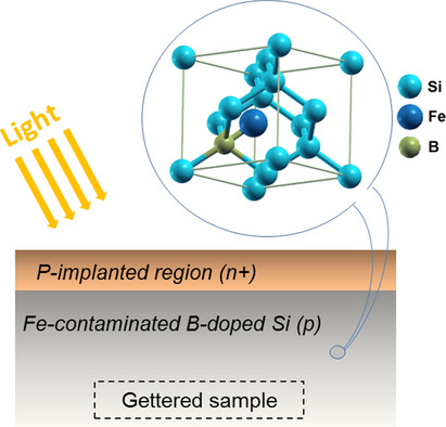
Behavior of iron–boron (FeB) pairs in boron-doped Czochralski silicon after extended gettering by phosphorus implantation at different temperatures is studied. The kinetic parameters of the light-induced dissociation of iron–boron pairs under standardized illumination, i.e., 1 and 0.5 sun, as well as the characteristics of their formation in the dark, are determined.
The Photo-Elastic Constant of Silicon Reviewed in Experiment and Simulation
- First Published: 02 July 2019

The anisotropy Ape of the photo-elastic constant is reviewed in experiments and simulations for single-crystalline silicon. (100) Si wafers are diametrically loaded in different crystallographic orientations and studied by means of the plane polariscope scanning infrared depolarization (SIRD) imager. Ape introduced as the ratio of the piezo-optical coefficients (π11 − π12 − π44)/(π11 − π12 + π44) is determined to be (0.21 ± 0.01).
Iodine–Ethanol Surface Passivation for Measurement of Millisecond Carrier Lifetimes in Silicon Wafers with Different Crystallographic Orientations
- First Published: 17 June 2019
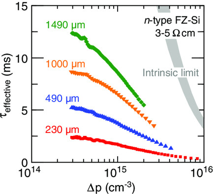
Excellent passivation of silicon surfaces is achieved via optimization of an iodine–ethanol (I–E) scheme. A robust method based on samples with different thicknesses cut from the same float-zone ingot is used to determine a lowest surface recombination velocity of 4.4 cm s−1 for (100)-orientation silicon. I–E is demonstrated to be superior to superacid-derived passivation for (111)-orientation silicon surfaces.
Oxygen Precipitation Properties of Nitrogen-Doped Czochralski Silicon Single Crystals with Low Oxygen Concentration
- First Published: 07 June 2019

The oxygen precipitation in the as-grown defect-free region of nitrogen-doped Czochralski silicon single crystals with low oxygen concentrations ([Oi]) is investigated. Oxide precipitates are completely suppressed at an [Oi] value below 3 × 10¹⁷ atoms cm−3. A thermodynamic model for oxygen precipitation indicates that the growth onset temperature of embryos is extremely low to grow as stable oxide precipitates.
Light-Induced Degradation in Annealed and Electron Irradiated Silicon
- First Published: 05 June 2019
The composition of the boron–oxygen-related light-induced degradation (BO-LID) defect is an unresolved issue. Recently, BO-LID is suggested to be due to the ASi-Sii-defect. Thus, creation and discreation of BO-LID is governed by the interstitial silicon concentration. Annealing and electron beam irradiation are applied. BO-LID is created in oxygenated silicon after 4 h annealing at 650 °C and discreated by 16 h annealing at 1050 °C.
Transport of Charge Carriers along Dislocations in Si and Ge
- First Published: 06 June 2019
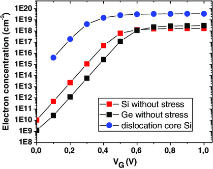
Experimental observations and quantum mechanical device simulations point to different electronic properties of the dislocations in Si and Ge. A supermetallic conduction behavior and strain-induced carrier confinement (1D electron gas) are proved for dislocations in Si. Both are not confirmed for Ge. The carrier confinement results in higher electron concentrations on dislocation cores in Si than on dislocations in Ge.
Lifetime Control in Irradiated and Annealed Cz n-Si: Role of Divacancy-Oxygen Defects
- First Published: 04 June 2019
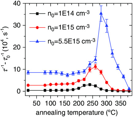
The behavior of the nonequilibrium charge carrier lifetime in Czochralski-grown n-Si after irradiation and subsequent annealing (20–380 °C) are investigated. It is shown that change in lifetime in the annealing range of 180–380 °C is caused by the divacancy-oxygen (V2O) complexes. The values of hole capture cross-section and the parameters of V2O formation and annealing are determined.
Features of the Formation of the BiBs Defect in Si
- First Published: 06 June 2019
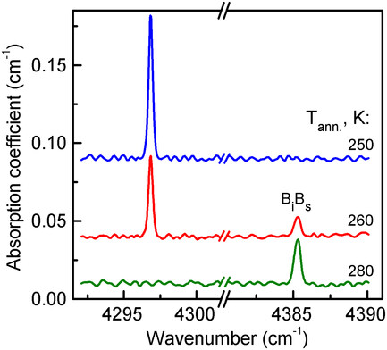
The electronic transition at 4296.8 cm–1 is revealed in the absorption spectra of boron-doped Si irradiated at 80 K with 5 MeV electrons. The disappearance of the defect responsible for the registered line upon annealing is accompanied by the emergence of the BiBs complex. The found defect is identified as a precursor of a stable configuration of BiBs.
Observation of the Stacking Faults in In0.53Ga0.47As by Electron Channeling Contrast Imaging
- First Published: 25 June 2019
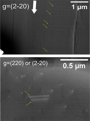
Two types of stacking faults (SFs) in InGaAs are observed by electron channeling contrast imaging (ECCI). By comparing their shapes and invisibility conditions, Frank SFs, followed by a Lomer–Cottrell lock and glissile SFs with two Shockley partial dislocations, can be distinguished. Transmission electron microscopy (TEM) and atomic force microscopy (AFM) are also performed to validate the results in this study.
Role of Impurities in Silicon Solidification and Electrical Properties Studied by Complementary In Situ and Ex Situ Methods
- First Published: 11 July 2019

Grain structures and electrical properties are studied in silicon contaminated with impurities. The presence of carbon induces a higher amount of grain nucleation, resulting in the high-order twin and random angle grain boundaries. Cu can lead to solid–liquid interface destabilization. Lifetime maps demonstrate the influence of impurities on the electrical activity in relation to the crystallographic defects and grains.
Separation of Individual Thermal Double-Donor Levels by Laplace Deep-Level Transient Spectroscopy
- First Published: 04 June 2019
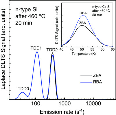
Heating of silicon with high oxygen concentrations at around 450 °C generates thermal double donors (TDD). The energy levels up to 17 donors are very similar, which makes it impossible to separate the single species by deep level transient spectroscopy (DLTS) measurements. Using high-resolution Laplace DLTS, the first three TDDs are resolved, and their properties are determined.
Laplace DLTS
Detection of Sulfur-Related Defects in Sulfur Diffused n- and p-Type Si by DLTS
- First Published: 04 June 2019
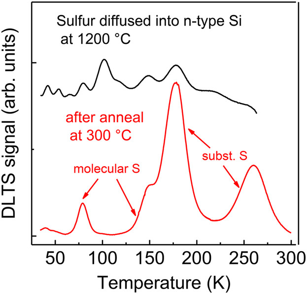
Sulfur doped Si samples show after diffusion several DLTS levels. Only an anneal at 300 °C generates the well-known levels of the substitutional S and S2 donors. Some of the levels in the sample after diffusion coincide with the S and S2 levels but are shown to have different origins.
Copper-Nickel Complexes
Electrically Active Copper–Nickel Complexes in p-Type Silicon
- First Published: 04 June 2019
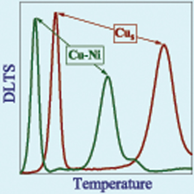
The interaction of highly mobile transition metal ions with substitutional impurities in Si at around room temperatures is of major concern in device technology. The fundamental aspect of this work is related to the question of how precipitate formation starts. The binding of fast diffusing Ni and Cu interstitials with substitutional Cu in Si is chosen to learn about the defect reactions.
Unusual Polarization Dependence of Dislocation-Related Luminescence in n-GaN
- First Published: 17 June 2019
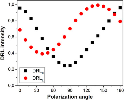
Polarization dependence of dislocation-related luminescence (DRL) from a-screw dislocations introduced by local plastic deformation in n-GaN is found to be different for two components of DRL spectral doublet: the high-energy component is polarized parallel, whereas the low-energy component is inclined under the angle of about 40° to the dislocation line.
Diffusion of Phosphorus and Boron from Atomic Layer Deposition Oxides into Silicon
- First Published: 11 July 2019
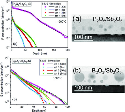
Transmission electron microscopy (TEM) investigations show that dopant-oxide stacks such as P2O5/Sb2O5 and B2O3/Sb2O5 grown by atomic layer deposition (ALD) on silicon transfer during annealing to silicon oxide with embedded spherical, partially crystalline particles. Dopant diffusion from these layers leads to shallow profiles with high phosphorus (>1 × 1020 cm−3) and boron (>1 × 1021 cm−3) concentrations in silicon. A numerical analysis of the diffusion process is provided.
Thermal Stability of Defect-Enhanced Ge on Si Quantum Dot Luminescence upon Millisecond Flash Lamp Annealing
- First Published: 11 July 2019
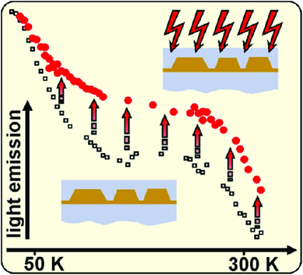
The influence of millisecond flash lamp annealing (FLA) on epitaxial, defect-enhanced quantum dot (DEQD) light emitters is investigated, demonstrating the thermal robustness of these group-IV nanostructures and improved light emission yield over a large range of temperatures.
Preparation Techniques for Cross-Section Transmission Electron Microscopy Lamellas Suitable for Investigating In Situ Silicon–Aluminum Alloying at Grain Boundaries in Multicrystalline Silicon
- First Published: 12 June 2019
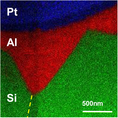
In situ heating transmission electron microscopy (TEM) possesses even stronger requirements on sample preparation than conventional TEM. Therefore, this article presents novel methods for tackling this issue. Using the example of Al-Si alloying at grain boundaries, the capabilities of the methods to produce low contamination, site-specific lamellas from ion beam sensitive samples are examined.
Passivation of Detector-Grade Float Zone Silicon with Atomic Layer Deposited Aluminum Oxide
- First Published: 11 July 2019
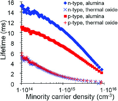
Passivation of detector-grade float-zone (FZ) silicon with aluminum oxide (Al2O3) is studied, focusing on the effect of post-annealing temperature on carrier lifetimes and film properties. It is confirmed that Al2O3 provides excellent surface passivation on high-resistivity FZ-Si substrates. Bulk lifetime degradation during low-temperature annealing can be prevented by high-temperature treatment only in p-type substrates.
Defects in Oxidized p-Type Si Wafers Observed by Surface Photovoltage Spectroscopy
- First Published: 08 June 2019
Oxidation processes under different conditions can lead to the formation of electrically active defects in silicon wafers. A significant degradation of minority carrier diffusion length is observed in wet oxidized p-type silicon wafers by using the surface photovoltage technique. Such a degradation is not detected in wet oxidized n-type silicon wafers. Different models are suggested to explain this degradation.
Platinum–Copper Defects in Silicon
- First Published: 04 June 2019
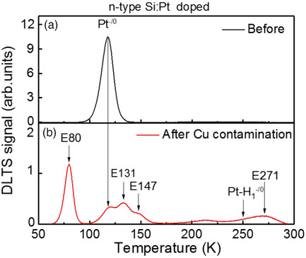
Cu is introduced into n-type Si at room temperature from a polishing slurry. Interstitial Cu is shown to create new defects with a substitutional Pt. The electrical parameters of the defects are determined and tentatively identied with complexes of one substitutional Pt atom and n = 1 to 4 interstitial Cu atoms (PtS (Cui)n).
Radiation Defects Created in n-Type 4H-SiC by Electron Irradiation in the Energy Range of 1–10 MeV
- First Published: 02 July 2019
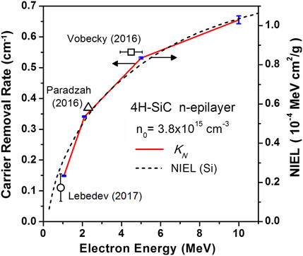
Radiation damage in 4H-SiC produced by 1.05–10 MeV electrons is investigated by deep-level transient spectroscopy. Introduced damage is very similar in the whole energy spectrum; however, with increasing energy, the number of simple defects saturates, and the amount of defect clusters grows. The carrier removal rate caused by the introduced acceptor centers follows well the classical nonionization energy loss scaling.
Etch Pit Density Reduction in POCl3 and Atmospheric Pressure Chemical Vapor Deposition-Gettered mc-Si
- First Published: 08 July 2019
The measured etch pit density in mc-Si material is shown to be reduced by P-gettering. Various pieces of evidence are presented, suggesting that defect etching does not reveal impurity-lean dislocations.
Novel Way to Assess the Validity of Czochralski Growth Simulations
- First Published: 04 June 2019
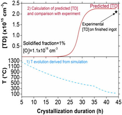
The temperature field across a Czochralski throughout crystallization is a key quantity governing process (energy uptake) or material (thermal stress, defects) parameters. It is typically derived using simulations and hard to confirm experimentally. A post-growth method is proposed to validate calculated temperature field evolution, based on the measurement of thermal donors, a relic of the ingot thermal history.
Spectroscopic Characterization of Silicon Wire-Like and Porous Nanolayers in the Process of Metal-Assisted Chemical Etching of Single-Crystal Silicon
- First Published: 27 July 2019
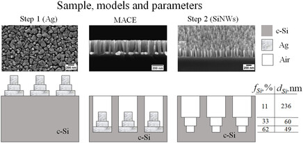
The preparation of c-Si nanowires and porous nanolayers using the two-stage metal-assisted chemical etching process is studied. The structures are characterized in all stages of the process by spectroscopic ellipsometry and using the following two approaches: 1) with the complex pseudo-dielectric function determined and analyzed and 2) with parameters of simulated multilayer structures determined in the effective medium approximation.
P-type Upgraded Metallurgical-Grade Multicrystalline Silicon Heterojunction Solar Cells with Open-Circuit Voltages over 690 mV
- First Published: 04 June 2019
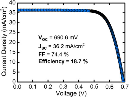
Herein, a multi-stage defect-engineering approach is developed, incorporating gettering and hydrogenation to improve the quality of low-cost silicon wafers. This technique is applied to p-type upgraded metallurgical-grade multicrystalline silicon wafers from the edge of the silicon cast. Silicon heterojunction solar cells are fabricated with these defect-engineered wafers, achieving an impressive open circuit of >690 mV and efficiency of 18.7%.
Impurity Gettering by Boron- and Phosphorus-Doped Polysilicon Passivating Contacts for High-Efficiency Multicrystalline Silicon Solar Cells
- First Published: 04 June 2019
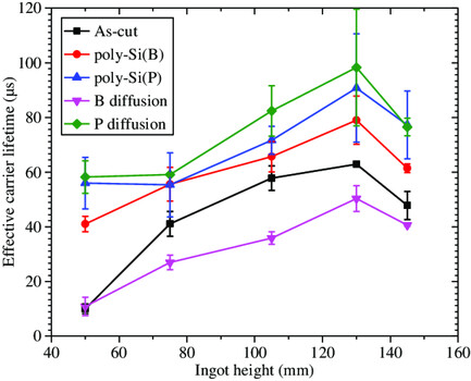
The effective carrier lifetime (at an excess carrier density of 7 × 1015 cm−3) of the as-cut and as-treated samples, which are extracted from five locations (from bottom to top) of a high-performance multicrystalline silicon ingot, are characterized. The substantial lifetime improvements highlight the strong external gettering effect achieved by both p-type and n-type poly-Si passivating contact fabrication processes.
Application of the Concept of Lifetime-Equivalent Defect Density in Defect Systems Comprising a Multitude of Defect Species
- First Published: 19 July 2019
The specific impact of different defect species in crystalline silicon on the injection-dependent excess carrier lifetime is used to identify defect species and analyze their properties. Especially, the lifetime-equivalent defect density as a measure of the actual defect density helps to distinguish different defect species encountered during light-induced degradation phenomena.
The Effects of Aluminum Gettering and Thermal Treatments on the Light-Emitting Properties of Dislocation Structures in Self-Implanted Silicon Subjected to Boron Ion Doping
- First Published: 08 August 2019
The temperature dependence of dislocation-related photoluminescence in silicon samples with dislocations created by self-ion implantation with subsequent annealing and additional boron doping, is investigated. Aluminum gettering and identical heat treatments make it possible to significantly improve luminescence temperature dependence and ensure the maintenance of dislocation-related luminescence up to 270 K. The observed effect is clearly associated with boron doping.
Near-Surface Defect Control by Vacancy Injecting/Out-Diffusing Rapid Thermal Annealing
- First Published: 10 July 2019
A simulation model for dissolution of octahedral bulk micro defects (BMD) in pure argon or oxidizing ambient is developed. The model is capable of predicting under which rapid thermal annealing (RTA) conditions the BMD nuclei dissolution occurs. In addition, the impact of the RTA process sequence on the homogeneity of the BMD-denuded zone is evaluated.
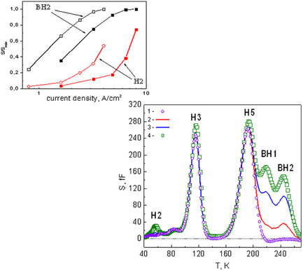
Room-Temperature Ni Interaction with Deformation-Induced Defects in Si: A DLTS Study
- First Published: 03 July 2019
The deep-level transient spectroscopy (DLTS) technique is used to study the room-temperature interaction of the extended defects introduced in Si by plastic deformation with the mobile Ni species. A special deformation geometry enables to separate contributions from the dislocations and the dislocation trails. It is shown that Ni decorates the extended defects, increasing the concentration of deep-level centers by an order of magnitude.
Peculiarity of Electric Properties of Oxygen-Implanted Silicon at Early Precipitation Stages
- First Published: 28 June 2019
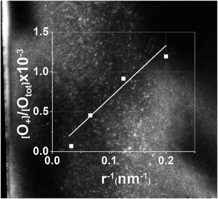
Embedded positive charge of oxygen precipitates (OPs) formed by thermal treatment of oxygen-implanted silicon decreases inversely proportional to their size, giving evidence of the charge localization in thin nonstoichiometric shell of OPs. The treatment at 700 °C results in the formation of nanosized defects and in an inhomogeneous electric structure of the oxygen-implanted region.
First Principles Study of the Stability and Diffusion Mechanism of a Carbon Vacancy in the Vicinity of a SiO2/4H–SiC Interface
- First Published: 26 July 2019
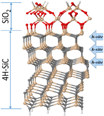
The majority of electronically active defects in SiC are located deep within the bandgap, thereby degrading the carrier transport properties of SiC. This study compares the diffusion of a carbon vacancy in different (0001)-layers relative to a SiO2/SiC interface using the density-functional theory simulations. The results show that vacancies in the upper layers are stabilized due to stronger bonding and interfacial relaxation.
Formation of a Bistable Interstitial Complex in Irradiated p-Type Silicon
- First Published: 18 June 2019
The influence of the injection of minority charge carriers on the formation of a divalent bistable defect (DBH) is investigated. The production of such bistable defect is enhanced in materials with a high ratio of boron to carbon concentrations. It is concluded that the DBH defect has inverse occupancy level ordering in its stable configuration.
Sign up for email alerts
Tools
![]()
In 2022, the youngest family member physica status solidi (RRL) – Rapid Research Letters is turning 15 years. To celebrate this milestone, we present a new virtual collection with invited articles.
![]()
As we celebrate the 60th anniversary year of the physica status solidi family, click here to access our continuously updated collection of invited articles written by authors and partners of the pss journals.