Diffusion of Phosphorus and Boron from Atomic Layer Deposition Oxides into Silicon
Abstract
Oxides containing group III or group V elements (B2O3/Sb2O5 and P2O5/Sb2O5) are grown by plasma-assisted atomic layer deposition (ALD) on single-crystalline silicon and serve as dopant sources for conformal and shallow doping. Transport phenomena in ALD-oxide–Si structures during rapid thermal annealing (RTA) are investigated subsequently by X-ray photoelectron spectroscopy (XPS), transmission electron microscopy (TEM), and secondary ion mass spectrometry (SIMS). The XPS and TEM analyses of the annealed ALD-oxide–Si structures demonstrate that the ALD oxide converts to a silicon oxide and partially evaporates during annealing. In addition, dopant-containing, spherical, and partially crystalline particles form in the oxide, and Si-P precipitates at the oxide–Si interface. After diffusion annealing at 1000 °C, the SIMS analyses reveal phosphorus and boron concentration profiles in the silicon substrate with maximum concentrations exceeding their solid solubility limits by roughly one order of magnitude. Experimental doping profiles of phosphorus and boron in silicon are compared with simulation results, considering a slight injection of self-interstitials and dynamical defect clustering.
1 Introduction
The technology of high-density 3D integrated semiconductor devices requires ultra-shallow junctions with sufficiently low sheet resistances.1, 2 Increasing demands for continuously scaled-down device dimensions drive the improvement of doping technologies for narrow 3D structures like FinFETs3 or nanowires.4, 5 Particularly 3D applications featuring high spatial ratios are critical with respect to the conformity of the doping process.6 Conventionally, dopants are introduced in the semiconductor industry by low-energy (<5 keV) ion implantation.7, 8 However, damage-related phenomena including transient enhanced diffusion (TED) and transient activation during dopant activation9-11 as well as ion-beam shadowing effects cannot be fully avoided.6, 12 To prevent these implantation-related problems, the deposition of a dopant source followed by a drive-in process could be a viable alternative. For the deposition of a dopant source, methods like monolayer doping (MLD),13, 14 chemical vapor deposition (CVD),15, 16 and plasma-assisted atomic layer deposition (ALD)17-19 have been reported. MLD may offer conformal doping of 3D structures, but it is limited in the range of dopant density and depth.13 ALD is one of the most promising candidates compared with CVD techniques20 due to its already demonstrated conformity, uniformity, controllability over material thickness and composition, low impurity contamination, low growth temperature (<350 °C), and radiation-free processing.19, 21, 22 The use of ALD-grown boron- and phosphorus-doped dopant sources has been demonstrated already for the shallow doping of silicon.23-27 In order to be able to optimize the doping processing conditions and control dopant diffusion according to the requirements of advanced 3D nanostructered devices, it is necessary to understand the mechanisms governing dopant diffusion in silicon as well as in covering oxides.
In this work, dopant transport phenomena from ALD-grown oxides into Si were investigated. The chemical structure and the composition of ALD oxides were studied after annealing by a combination of characterization techniques. The experimental doping profiles were compared with numerical simulations. The models and diffusion parameters implemented in the Sentaurus Process28 of Synopsys were completed for diffusion and segregation in the oxide, self-interstitial injection at the interface, and dynamic clustering of dopants to reproduce the experimental results.
2 Experimental Section
The deposition experiments were realized in a single ALD reactor manufactured by Sentech Instruments GmbH, Berlin. It was equipped with an “epilogos” inductively coupled (ICP) microwave plasma source placed on top of the reactor and operated at 2.55 GHz and 50 W of output power. The plasma was generated inside two parallel quartz glass tubes wherein the oxygen for the plasma step flowed into the reactor. Phosphorus oxide (P2O5) and boron oxide (B2O3) films with different thicknesses were grown on the crystalline silicon by ALD. Due to the instability of B2O3 and P2O5 films in air,25, 27 they were capped in situ with ALD-grown Sb2O5 layers for ex situ investigation.23 The temperature of the Si substrate during growth was 200 °C. Halogen-free precursors were used for the deposition processes, tris(dimethylamido)borane (B(NMe2)3) for boron oxides, tris(dimethylamido) antimony (Sb(NMe2)3) for antimony oxides, and tris(dimethylamido)phosphine (P(NMe2)3) for phosphorus oxides.
For the investigations, p-type, boron-doped, and n-type, phosphorus-doped, 710 μm thick <100> Cz-Si wafers with resistivities of 5–22 Ωcm and 8–12 Ωcm were used, respectively. Prior to the ALD process, the wafers were cleaned using standard Radio Corporation of America (RCA) chemical cleaning. In order to create the pn-junctions, the dopants were driven into silicon by rapid thermal annealing (RTA) in 1 bar of N2 at 1000 °C for annealing times in the range of 4–64 s. A ramp of 15 °C s−1 was used for heating and cooling in the temperature range of 700–1000 °C. The accuracies of the temperature and time measurements in our RTA setup were ±5 °C and ±0.5 s, respectively. The oxide thicknesses were measured before and after annealing by ellipsometry in the wavelength range from 360 to 800 nm. To study thermal stability, the chemical structure of the ALD-grown dopant-containing oxides, and the influence of oxide thickness on the dopant profiles of silicon, five sets of samples with different oxide stacks were prepared and investigated; see Table 1.
| Set | ALD-grown oxide thickness [nm] | RTA time [s] | ||
|---|---|---|---|---|
| B2O3 | P2O5 | Sb2O5 | ||
| 1 | 64 | 20 | ||
| 2 | 81 | 64 | 20 | |
| 3 | 28 | 63 | 20 | |
| 4 | 10 | 20 | 4/16/64 | |
| 5 | 10 | 20 | 4/16/64 | |
The resulting doping profiles were characterized by secondary ion mass spectrometry (SIMS). SIMS was performed by the Institute of Electronic Materials Technology (ITME) in Warsaw on selected samples after chemical removal of the diffusion source, employing a CAMECA SC Ultra instrument at ultra-high vacuum conditions and using a net energy of 90 eV for the Cs+ sputtering ions. The diameter of the sputter craters was 500 μm and the depth resolution was 1.2 nm. To estimate the electrically active part of the incorporated dopants, sheet resistance values were determined by four-point probe measurements on the same samples.
The structural properties of the annealed samples were characterized by cross-sectional transmission electron microscopy (TEM). Besides bright-field imaging, high-resolution TEM was performed with an image Cs-corrected FEI Titan 80–300 microscope that operated at an accelerating voltage of 300 kV. High-angle annular dark-field scanning transmission electron microscope (HAADF-STEM) imaging and spectrum imaging analysis based on energy-dispersive X-ray spectroscopy (EDXS) were performed at 200 kV with a Talos F200X microscope equipped with a field-emission gun (X-FEG) electron source and a Super-X EDXS detector system (FEI). Prior to TEM analysis, the specimen mounted in a high-visibility low-background holder was placed for 2 s into a Model 1020 plasma cleaner (Fischione) to remove possible contamination. Classical cross-sectional TEM specimens of the annealed ALD-oxide/Si stacks were prepared by sawing, grinding, polishing, dimpling, and final Ar ion milling. Chemical analysis of the oxides was also performed by X-ray photoelectron spectroscopy (XPS) using a monochromatic Al-Kα radiation X-ray source and hemispherical energy analyzer with a 2D delay-line detector. The typical sampling depth of the XPS analysis technique was less than 10 nm. The analyzed spot size was 400 μm. For depth profiling, the surface was repeatedly sputter-etched by Ar+ ions with an energy of 5 keV, and XPS spectra were taken after every etching cycle. The modeling of dopant diffusion in silicon from ALD oxides was carried out with Sentaurus Process of Synopsys.
3 Results and Discussion
3.1 X-Ray Photoelectron Spectroscopy Analysis
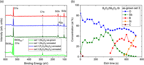
Figure 1a shows the XPS spectra of the as-grown sample from set 1 and of the annealed samples from the sets 1, 2, and 3. For the as-grown sample, three peaks at the binding energies of 540.6 and 530.8 eV as well as 284.8 eV are observed, which are attributed to Sb 3d3/229 and Sb 3d5/230 in a Sb-O environment of Sb2O5 as well as elemental C1s31 peaks, respectively. However, it is possible that antimony oxide is a mixture of Sb2O3 and Sb2O5.32 The O1s33 (around 532 eV) peak overlaps with the Sb 3d5/2 peak which is the most intense photoelectron peak from Sb, as indicated in Figure 1a. The as-grown spectrum of set 1 is typical for all as-grown samples, since the Sb2O5 films on top shield the underlying layers. The spectral analysis of the annealed samples reveals O1s, Si2p, and Si2s signals instead of antimony peaks (see Figure 1a). The O1s peak originates from SiOx structures and Si2s/Si2p34 peaks at binding energies of 154.8/103.7 eV from the SiO2 bond. Furthermore, phosphorus — as the P2p signal corresponding to the characteristic of the P-O bond at a binding energy of 135.5 eV35 — was detected in the annealed samples of the sets 2 and 3. The presence of phosphorus in the B2O3/Sb2O5-Si samples is surprising and can be explained only by contamination during the ALD or RTA processes. To check for possible contamination during the ALD process, the as-grown B2O3/Sb2O5-Si sample was analyzed by XPS depth profiling, as shown in Figure 1b. The quantification of the observed elements in the films was done by integrating the peak area intensities of the elements and the corresponding atomic sensitivity factors. The only contamination found in the as-deposited Sb2O5 film was adventitious carbon near the surface due to the exposure of the sample to air. The film on the sample surface consists of antimony and oxygen, below which a boron- and oxygen-containing layer is observed. There is no evidence for phosphorus, neither in the as-grown Sb2O5 film, nor in the as-grown B2O3 film. Therefore, we conclude that the B2O3/Sb2O5-Si samples were contaminated during the drive-in process by residual phosphorus from the previous RTA annealing of the P2O5/Sb2O5-Si samples. The oxide composition at the surfaces of the annealed samples was determined by XPS analysis to be close to SiO2C0.5 for the Sb2O5-Si sample, to SiO2.8C0.4P0.2 oxide for the P2O5/Sb2O5-Si sample, and to SiO2.2C0.4P0.01 oxide for the B2O3/Sb2O5-Si sample. This indicates that the full ALD-oxide stack was transformed to silicon oxide. The carbon contamination of the oxides is caused by adventitious carbon.
3.2 Transmission Electron Microscopy Analysis
The samples of sets 1, 2, and 3 were studied by cross-sectional TEM analysis, as shown for the annealed Sb2O5-Si, P2O5/Sb2O5-Si, and B2O3/Sb2O5-Si samples in Figures 2, 3, and 4, respectively. Whereas the darker regions in the bright-field TEM images of Figures 2a, 3a, and 4a represent the single-crystalline silicon substrate, the brighter layers on top are associated with the oxides. Their thicknesses decrease during annealing from 91 to 65 nm for the B2O3/Sb2O5-Si sample, from 145 to 55 nm for the P2O5/Sb2O5-Si sample, and from 64 to 9 nm for the Sb2O5-Si sample. Obviously, during annealing, the B2O3/Sb2O5, P2O5/Sb2O5, and Sb2O5 films partly evaporate. In particular, the evaporation rate for the B2O3/Sb2O5 oxide is lower than that for the P2O5/Sb2O5 or Sb2O5 films. Taking a closer look at the oxides, the high-resolution images in Figures 2b, 3b, and 4b indicate the presence of spherical, partially crystalline particles embedded in an amorphous matrix. There are more and larger particles in the B2O3/Sb2O5-Si sample than in the P2O5/Sb2O5-Si or in the Sb2O5-Si sample. Particles’ diameters range from 3 to 10 nm for the Sb2O5-Si sample, from 5 to 30 nm for the P2O5/Sb2O5-Si sample, and from 5 to 70 nm for the B2O3/Sb2O5-Si sample. Particle formation can occur during the cooling-down process because of the supersaturation of dopant atoms in the oxide.

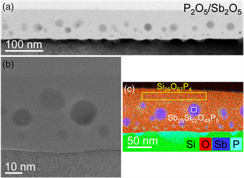
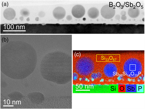
The chemical composition of the spherical particles and the surrounding matrix was determined by EDXS analysis in the scanning TEM mode. The obtained element distributions are displayed in Figures 2c, 3c, and 4c. Whereas the matrix was analyzed to be pure SiO2 (Figure 4c) or SiO2 containing a small amount of phosphorous (Figure 3c), the particles in the oxide resulted in the following compositions, as exemplarily determined for selected regions: Sb66Si14O19P1 in the B2O3/Sb2O5-Si sample (Figure 4c) and Sb25Si22O48P5 in the P2O5/Sb2O5-Si sample (Figure 3c). For the Sb2O5-Si sample, it is difficult to determine the composition of spherical particles, as they superimpose with the surrounding oxide matrix in the 2D projections obtained by conventional TEM analysis (Figure 2c). It should be mentioned that the boron concentration in all samples is below the detection limit. The accumulation of phosphorus is assumed to eventually result in the formation of Si-P precipitates observed at the oxide-Si interfaces of the samples of the sets 2 and 3. This is in agreement with the observed formation of SiP precipitates at the interface of silicon- and phosphorus-containing glasses grown by a POCl3 process.36-38 In such a ternary system, a higher amount of phosphorus atoms than expected from the binary solid solubility is introduced from the phosphorus glass to silicon. As the (binary) solubility of a dopant in silicon we denote the total concentration of this dopant in silicon in equilibrium with the respective impurity phase (either a pure dopant phase or a dopant silicide). The solubility concentration of the dopant in silicon includes substitutional and interstitial dopants, dopant complexes with intrinsic point defects, as well as small clusters comprising dopants and possibly intrinsic point defects. In turn, the supersaturation of total phosphorus concentration with respect to binary solid solubility in Si is expected thermodynamically to lead to the nucleation of SiP precipitates, i.e., of small volumes with an SiP composition, within the Si matrix. In the Si matrix around the precipitates, the total phosphorus concentration is in a steady state, slightly higher than binary solid solubility, and reduces toward binary solubility as the SiP precipitates grow in size. The phosphorus atoms in the SiP precipitates and in the Si matrix around them add to the chemical phosphorus concentration measured, e.g., by SIMS. However, it should be noted that SiP precipitation is a kinetically limited phenomenon and in none of our samples, precipitates, clusters, or structural defects were found deeper inside the Si substrate.
3.3 Secondary Ion Mass Spectroscopy Results and Simulation of Diffusion Profiles
In Figures 5a,b, the phosphorus and boron profiles obtained by SIMS measurements on the samples of sets 2 and 4 and of sets 3 and 5 are shown, respectively. A comparison of the sets 2 (81 nm of P2O5) and 4 (10 nm of P2O5) for phosphorus diffusion indicates a strong correlation of peak concentration with the thickness of the as-grown dopant oxide. We associate this finding with the strong evaporation of phosphorus oxide, see earlier, which depletes thinner oxides faster than thicker ones. At the same time, we see a strong correlation of the penetration depth with the thickness of the as-grown dopant oxide. Particularly, the correlation between oxide thickness and penetration depth, though weaker, is also seen for the sets 3 (28 nm of B2O3) and 5 (10 nm of B2O3) for boron diffusion. An increase in the drive-in time from 4 to 64 s leads to an increase in the diffusion depth from 50 to 95 nm for the phosphorus profiles of set 4 and from 60 to 75 nm for the boron profiles of set 5. The near-surface concentrations measured by SIMS exceed the solid solubility limit at 1000 °C for boron (≈1.2 × 1020 cm−3)39 by roughly an order of magnitude in the sets 3 and 5 as well as for phosphorus (≈4.3 × 1020 cm−3)40 in set 2. However, even for the samples of set 4, the phosphorus concentration close to the surface reaches its solubility limit. The dopant concentration in silicon close to the interface at the origin of the depth scale does not vary noticeably with time for the samples of the sets 4 and 5. This indicates that the dopant source was not depleted within the 64 s-long annealing process, even though the dopant oxide thickness was only 10 nm. It should be noted that the observed boron concentration in silicon is about one order of magnitude higher than that previously reported for ALD of B2O3 oxides.26, 27 The SIMS profiles of phosphorus and antimony in the boron-doped samples, as well as of antimony in the phosphorus-doped samples, are about three to four orders of magnitude lower in concentration than the main dopant concentration (not shown here). The oxygen concentration measured by SIMS was below 3 × 1018 cm−3 in all investigated samples.

Taking the XPS, TEM, and SIMS results into account, the diffusion of boron or phosphorus from ALD oxides into silicon can be described as follows. During the heating-up process, the ALD oxides melt, so they are liquid at temperatures above 600 °C41-43 and start to partially evaporate. The liquid dopant oxide also reacts with silicon so that a ternary (Si-O-P or Si-O-B) or a quaternary liquid oxide phase (Si-O-Sb-P or Si-O-Sb-B) forms. During the cooling-down phase, precipitates form in the oxide due to dopant supersaturation accompanied by very high diffusion coefficients in the liquid phase. In addition, SiP precipitates formed at the interface between the oxide phase and silicon. From the oxide phase, phosphorus or boron diffuses into silicon. There, the concentration at the interface is determined by the segregation coefficient of the respective dopant between the oxide and silicon phases. As indicated earlier, this concentration exceeds the binary solid solubility of the dopant in silicon. However, no dopant precipitates, clusters, or other structural defects were found by TEM to have formed in silicon. On the other hand, on the basis of sheet resistance measurements performed after diffusion, only small fractions of dopants in silicon were found to be electrically active. Accordingly, we expect the diffusion of dopants in silicon to be accompanied by significant clustering which retards the effective diffusion of dopants and reduces the concentration of the respective majority charge carriers. Other phenomena to be considered are the dependence of the concentrations of mobile complexes of dopants with intrinsic point defects on the charge-carrier concentrations as well as transport particularly of self-interstitials via dopant-self-interstitial pairs into the bulk which leads to an enhancement of the concentration of self-interstitials and to an enhanced dopant diffusion there. The chemical reaction of the liquid oxide phase with the silicon substrate may also lead to the injection of vacancies or interstitials into silicon, similar to the oxidation of silicon.
To take into account all these phenomena, the measured profiles and sheet resistances were modeled with the Sentaurus Process. For the simulation of boron and phosphorus profiles in silicon, the “react” diffusion model was used, which numerically solves differential equations for the dopant flux by considering charge-independent pairing reactions. The activation kinetic of dopants was modeled by a “transient” activation model, which calculates the dynamical defect-clustering considering the dopant atoms trapped in the clusters as immobile. Parameters, such as the forward-clustering reaction rate as well as the forward and backward reaction factors of the transient model, were adjusted to reproduce the shape of the SIMS dopant profiles and the experimental sheet resistance values.
In the simulations we assumed that the ALD oxide reacts on a much shorter timescale with the bulk silicon than the duration of the drive-in process. Accordingly, the resulting silicon oxide source was modeled as a highly doped SiO2 with a thickness as determined experimentally. The dopant concentrations and dopant diffusion coefficients in the highly doped SiO2 layer, as well as dopant solubility in silicon, were determined by reproducing the experimental doping profiles measured by SIMS. In silicon, dopant diffusion is determined by the dopant and intrinsic point defect (interstitials and vacancies) concentrations as well as their boundary conditions at the interface to the oxide. In the simulation, the “natural” boundary was used, which assumes that the fluxes of the self-interstitials and the vacancies at the oxide-Si interface are proportional to the respective oversaturation there. The segregation of dopants from the oxide source into silicon was modeled with a “two-phase segregation” model, assuming that the total dopant fluxes at the interface are balanced. It was considered that boron diffusion is governed by an interstitial mechanism whereas phosphorus is assumed to diffuse via vacancies and self-interstitials as well.44-46 The simulation was nominally carried out assuming the presence of an oxygen atmosphere in order to take into account the oxidation effect on diffusion. The values of dopant segregation and of oxygen partial pressure (≤0.4 atm.) were calibrated by reproducing the experimental dopant profiles. The model parameters used are listed in Table 2. They were obtained by adapting the default parameters of Sentaurus Process to best describe the experimental profiles. Prefactors and activation energies could not be determined independently. Accordingly, the parameters reflect particularly the processes at the peak temperature of 1000°C and to a lesser degree those at lower temperatures during ramping.
| Parameter | Dopant | |
|---|---|---|
| Boron | Phosphorus | |
| Dopant concentration in SiO2 [cm−3] | (1.0 ÷ 1.5) × 1022 | (0.95 ÷ 8.3) × 1021 |
| Dopant diffusion coefficient in SiO2 [cm−2] | 2.7 × 10⁻⁴exp(−3.3 eV (kT)−1) | 5.6 × 10⁻¹exp(−3.32 eV (kT)−1) |
| Solubility in Si [cm−3] | (6.5 ÷ 7.5) × 1020exp(−0.2 eV (kT)−1) | (4.5 ÷ 8.1) × 1020exp(−0.06 eV (kT)−1) |
The simulation results of phosphorus and boron diffusion are displayed in Figure 5 as lines together with the SIMS profiles. The simulated phosphorus and boron profiles agree well with the experiment. In the simulation, it was considered that large parts of the phosphorus and boron atoms are trapped in P3 and B4 clusters, respectively. Trapped phosphorus and boron concentrations are assumed to be electrically inactive. At high concentrations, the formation of a kink as well as of a flat high-concentration region in the phosphorus-doped samples was observed (see Figure 5a). In this concentration range, diffusion via phosphorus-vacancy pairs dominates.47-49 Similar to phosphorus, boron may introduce an oversaturation of self-interstitials in the bulk. This effect appears to be overestimated in the simulations since the simulated profiles of the samples of set 5 are deeper than the profiles from SIMS analysis. From the simulations, the fractions of electrically active dopants were estimated to be about 15% for phosphorus and 5% for boron (see Figure 5).
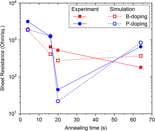
Figure 6 illustrates the dependence of sheet resistance on annealing time as extracted from simulations and measurements for phosphorus and boron diffusion. The simulated sheet resistances match the measurements well and follow the same trend, confirming a low activation ratio of boron and phosphorus. This indicates that the diffusion of boron and phosphorus from ALD oxides into silicon is affected by the formation of immobile dopant-defect clusters.
4 Conclusion
Diffusion of phosphorus and boron from ALD dopant-oxide stacks during drive-in annealing at 1000 °C into single-crystalline silicon was investigated. XPS and TEM analyses reveal a partial evaporation and complete transformation of the ALD-oxide stacks into silicon oxide during annealing. Furthermore, spherical, partially crystalline particles embedded in the oxide were found by TEM. The formation of Si-P precipitates was also observed in the P2O5/Sb2O5-Si and B2O3/Sb2O5-Si samples at the oxide-silicon interface. The chemical composition of the spherical particles determined by STEM-EDXS analysis is close to Sb66Si14O19P1 for the B2O3/Sb2O5-Si sample and to Sb25Si22O48P5 for the P2O5/Sb2O5-Si sample. Moreover, high-concentration shallow phosphorus (>1 × 1020 cm−3) and boron (>1 × 1021 cm−3) profiles in silicon were realized by the ALD oxides acting as diffusion sources. By simulations, the diffusion process of the dopants from ALD oxides was modeled and a set of parameters for process simulation was calibrated. Experimental phosphorus and boron profiles as well as sheet resistances were reproduced by numerical simulations considering dynamical dopant-defect clustering. It can be concluded from the simulations that a diffusion of phosphorus and boron as well as a low activation ratio of dopants in silicon are affected by the formation of immobile dopant clusters during the drive-in process. We expect that the activation ratio can be increased considerably by a millisecond or nanosecond flash or laser annealing.
Acknowledgements
This work was supported by the Deutsche Forschungsgemeinschaft (DFG) (Contracts FR 713/14-1 and KA 4358/1-1). The authors thank Romy Aniol for careful TEM specimen preparation. Furthermore, the use of HZDR Ion Beam Center TEM facilities and the funding of TEM Talos by the German Federal Ministry of Education of Research (BMBF, Grant No. 03SF0451) in the framework of HEMCP are acknowledged.
Conflict of Interest
The authors declare no conflict of interest.


