Journal list menu

 Issue
Issuephysica status solidi (a): Volume 217, Issue 12
Special Issue:Advanced Electromaterials
June 2020Guest Editor(s):
Export Citations
Download PDFs
Cover Picture
Hybrid Passivation for Foldable Indium Gallium Zinc Oxide Thin-Film Transistors Mediated by Low-Temperature and Low-Damage Parylene-C/Atomic Layer Deposition-AlOx Coating
- First Published: 18 June 2020
Thin-Film Transistors
In article number 1900832 by Shijie Zhan, Bo Hou, and co-workers, a parylene-C/AlOx hybrid passivation approach is introduced to reduce the damage during AlOx atomic layer deposition. This method enables a flexible transistor backplane matrix with remarkably improved bias stability.
Masthead
Editorials
Editor's Choice
Optimal Composition of ZnO/WO3 Composite Nanoparticle Gas Sensors
- First Published: 11 February 2020
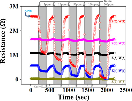
The effect of the ZnO/WO3 molar ratio on the response of ZnO/WO3 composite nanoparticle sensors to CO is investigated. The strongest response to 200 ppm CO is obtained by the 6:4 ZnO/WO3 composite sensor in this study, whereas a 5:5 ZnO/WO3 composite sensor showed the strongest response to gases in previous reports.
Original Papers
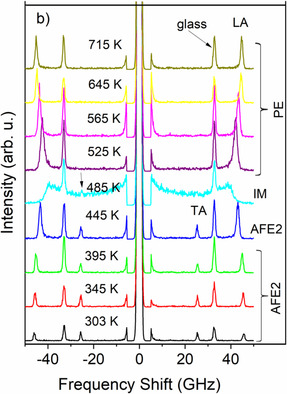
T* of Relaxor Ferroelectric (1 − x) Pb(Zn1/3Nb2/3)O3-xPbTiO3 Single Crystals Revisited Using Brillouin Spectroscopy
- First Published: 05 February 2020
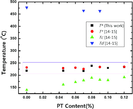
The intermediate temperature T* of Pb[(Zn1/3Nb2/3)1–xTix]O3 single crystals is investigated using Brillouin spectroscopy. The temperatures of the steepest descent of the half width of the longitudinal acoustic mode are nearly the same irrespective of composition, revealing universal feature of T* at which dynamic polar nanoregions are transformed into quasistatic ones.
Hybrid Passivation for Foldable Indium Gallium Zinc Oxide Thin-Film Transistors Mediated by Low-Temperature and Low-Damage Parylene-C/Atomic Layer Deposition-AlOx Coating
- First Published: 03 December 2019
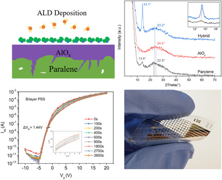
A parylene-C and aluminum oxide (AlOx) hybrid passivation approach are introduced to reduce the damage during AlOx atomic layer deposition. Based on Mott–Schottky and X-ray diffraction characterizations, the thin-film transistor (TFT) performance enhancement is attributed to doping density variation that results in high-performance depletion-mode indium–zinc–gallium–oxide TFT matrix to be operated on polyethylene naphthalate substrate with enhanced bias stability.
Morphology Effect of 1D ZnO Nanostructures Designed by Hydrothermal and Thermal Annealing for Fast Ultraviolet Photodetector Applications
- First Published: 21 April 2020
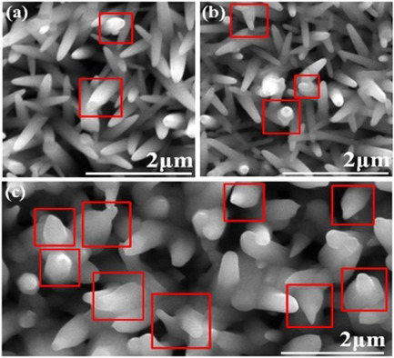
When the ZnO nanorods are grown using the hydrothermal method, interstitial oxygens are generated in the ZnO lattice. So, the decrease of the number of defects is necessary. Herein, the number of interstitial oxygens using thermal annealing is reduced, and it led to the improvement in the crystallinity and photosensitivity of ZnO nanorods compared with nonannealed ZnO nanorods.
Investigation on Hump Mechanism in Amorphous SiZnSnO Thin-Film Transistor Depending on Si Concentration
- First Published: 28 February 2020
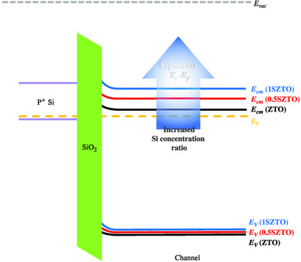
Amorphous SiInZnO thin films are fabricated according to the Si content, and their electrical properties are analyzed under various measurement conditions. It is confirmed that the nonideal transfer characteristics, at low Vds, may be caused by the bandgap changes. For the next generation of low-power devices, the bandgap between the electrode and the semiconductors requires consideration.
Effect of Sn Addition on Thermodynamic, Dielectric, Optical, and Acoustic Properties of Lead Hafnate
- First Published: 29 January 2020
Specific heat, dielectric properties, and domain structure studies in antiferroelectric PbHf1−xSnxO3 single crystals with three different concentrations (x = 0.08, 0.1, 0.23) are performed in function of temperature. Temperature- and composition (concentration of Sn ions)-induced phase transitions (PTs) are further investigated by Brillouin light scattering spectroscopy to deeply understand the dynamics of PTs in relation to domain structure and physical properties.
Enhanced Electrical Performance of Structurally Engineered Memristor Devices with Multi-Stacked Indium Zinc Oxide Films
- First Published: 21 March 2020
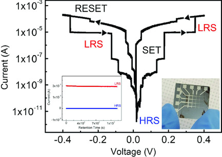
The crossbar array memristor with a structure of Al/three-multi-stacked indium zinc oxide/TiO2/Al exhibits uniformity and reproducibility of resistance switching behavior with low-resistance state and high-resistance state voltage sweeps, and show excellent retention performance over 2 × 10³ s. This research suggested that some other appropriate metal oxide thin films with good resistive switching performance can be used to prepare structurally enhanced memristor devices.
Transition Metals (Co or Ni) Encapsulated in Carbon Nanotubes Derived from Zeolite Imidazolate Frameworks (ZIFs) as Bifunctional Catalysts for the Oxygen Reduction and Evolution Reactions
- First Published: 21 April 2020
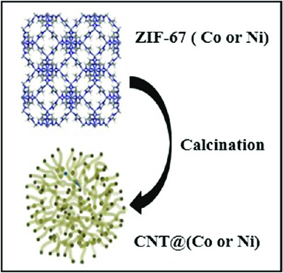
Co or Ni encapsulated in the carbon nanotubes [CNT@(Co or Ni)] was obtained via calcination of Co- and Ni-ZIF-67. The porous CNT@(Co or Ni) exhibits superior electrochemical performance when used as a cathode material for oxygen reduction reaction (ORR) and oxygen evolution reaction (OER).
Enhanced Electromechanical Properties of 0.65Bi1.05FeO3–0.35BaTiO3 Ceramics through Optimizing Sintering Conditions
- First Published: 20 March 2020
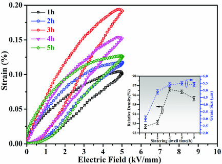
Pb-free 0.65Bi1.05FeO3–0.35BaTiO3 (BF–35BT) piezoceramics are synthesized via conventional solid-state reaction by varying sintering dwell time (ts) to study its effect on electromechanical properties. ts has a profound effect on grain size and density of composition, showing that for ts = 3 h, enhanced electromechanical properties are achieved with a maximum relative density of 96.61% and grain size of 5.41 μm.
Boron-Doped Single-Crystal Diamond Growth on Heteroepitaxial Diamond Substrate Using Microwave Plasma Chemical Vapor Deposition
- First Published: 11 February 2020
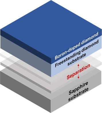
Herein, it is demonstrated that boron-doped diamond layer is grown on freestanding heteroepitaxial diamond substrates by microwave plasma chemical vapor deposition (MPCVD) to verify the high potential of large-size heteroepitaxial diamond as an ultimate semiconductor material.
Oxygen Vacancy Controlled SiZnSnO Thin-Film Inverters with High Gain
- First Published: 14 April 2020
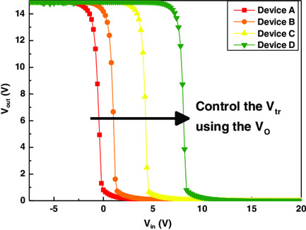
Herein, amorphous SiZnSnO (a-SZTO) thin-film transistors (TFTs) are fabricated and analyzed according to the oxygen partial pressure [p(O2)] ratio. The Vth moves to positive direction, as the p(O2) increases. In the inverter, the Vtr moves to positive direction as the p(O2) increases. It is possible to control the Vtr of n-type only inverter.
Phase Evolution, Microstructure, Electrical, and Magnetic Properties of Bi0.5(Na0.68K0.22Li0.10)0.5TiO3 Ceramics with Fe3+ Substitution
- First Published: 07 March 2020
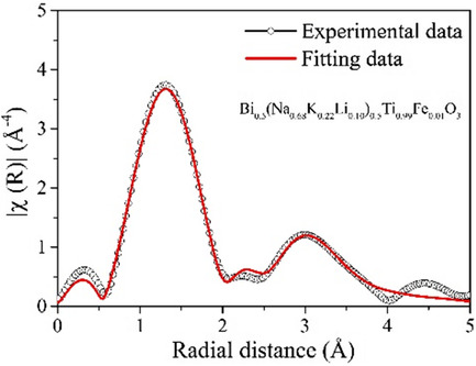
The substitution of Fe3+ into the Ti4+ sites leads to the oxygen vacancies formation, which can cause the lattice distortion. Excellent ferroelectric properties (Pr ≈ 26.8 μC cm−2, Ec ≈ 20.4 kV cm−1) and the highest normalized strain () of 386 pm V−1 are obtained in Bi0.5(Na0.68K0.22Li0.10)0.5Ti0.99Fe0.01O3 ceramic; the morphotropic phase boundary (MPB) composition where rhombohedral and tetragonal phases coexist with 51.3:48.7% ratio.
Ferroelectric and Piezoelectric Properties of BiFeO3-Based Piezoelectric Ceramics
- First Published: 06 January 2020
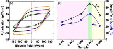
(1−x)Bi0.97Sm0.08FeO3−xBaTiO3 ceramics (with x = 0.00–0.05) are synthesized through the conventional solid-state reaction method. The remanent polarizaion of the furance cooled ceramic significantly enhances from 12 to 28.5 μC cm−2 with water quenching and BaTiO3 addition. High piezoelectric performace (d33 = 56 pC N−1 and d33* = 40 pm V−1) obatins for an optimum composition (with x = 0.03).
Dopant Activation of In Situ Phosphorus-Doped Silicon Using Multi-Pulse Nanosecond Laser Annealing
- First Published: 13 February 2020
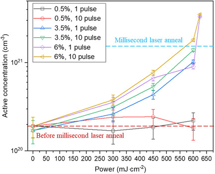
Nanosecond laser annealing is performed on in situ phosphorus-doped silicon in single- and multipulse modes. The active phosphorus concentration is increased with the laser power density and number of laser pulses and more phosphorus is activated with nanosecond lasers than with millisecond lasers. Moreover, almost all the incorporated phosphorus atoms are activated.
Comparison of Strain Characteristics and Contact Resistances of Heavily Phosphorus-Doped Si Formed by Phosphorus Implantation and In Situ Phosphorus-Doped Si Epitaxial Growth
- First Published: 18 March 2020
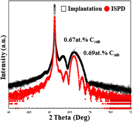
Comparison of the strain properties of phosphorus doped silicon formed by phosphorus implanted and in situ phosphorus-doped. The same level of strain is applied regardless of the doping method. This implies that phosphorus acting as a stressor is present, suggesting that stress can also be applied through the phosphorus implantation with laser spike annealing treatment to suppress diffusion.
Defect Generation Mechanism of Epitaxially Grown In Situ Phosphorus-Doped Silicon on Silicon (111) Substrate
- First Published: 03 March 2020
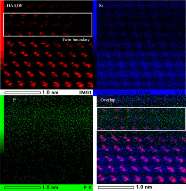
In situ phosphorus-doped (ISPD) silicon layer are epitaxially grown on silicon (100) and (111) substrates. The ISPD layer on the (111) silicon substrate exhibits more defects and they induce strain relaxation. Atomic resolution energy-dispersive X-ray spectroscopy (EDX) mapping results in a higher concentration of phosphorus at defects.
Thermolytic Deposition of MoS2 Nanolayer for Si Solar Cell Applications
- First Published: 24 March 2020
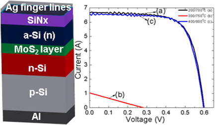
The thermolytic deposition is investigated for a large scale and direct synthesis of a MoS2 nanolayer on micro-pyramidal p-Si wafers for solar cell application. The MoS2 nanolayer shows a transition from an amorphous to a crystalline phase after the annealing process. The MoS2 based heterostructures in p-Si photovoltaic devices produce the photoconversion efficiencies of up to 11.47%.
Template-Free Synthesis and Growth Mechanism of Hollow Structure SnO2 and Fabrication of Core-Shell SnO2@ZnO
- First Published: 07 March 2020
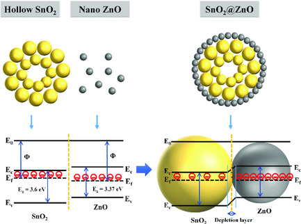
The hollow structure of tin oxide (SnO2) is synthesized without a template. The synthesis of the core-shell structure forms the heterojunction between SnO2 and zinc oxide (ZnO). The junction between SnO2 and ZnO changes the charge transfer and interfacial effects on the surface of the material. This structure can be applied to the field of gas sensors and photocatalysts.
Rare Metal-Free High-Performance Zinc–Tin Oxide Thin Film Transistors Using Efficient Energy Conversion of Microwave Annealing
- First Published: 03 March 2020
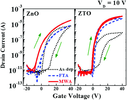
Herein, the efficient energy conversion of microwave annealing (MWA) on the electrical properties of rare metal-free zinc–tin oxide (ZTO) thin-film transistors (TFTs) is evaluated. Furthermore, the instabilities of gate bias temperature stress are also investigated. Compared with zinc oxide TFTs and furnace thermal-annealed devices, MWA-treated ZTO TFTs exhibit highly improved electrical and stability characteristics.
Metal Organic Frameworks as Tunable Linear Magnets
- First Published: 19 February 2020
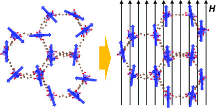
The magnetic properties of selected metal–organic frameworks (MOFs) are assessed using alternating current (AC)/direct current (DC) magnetic susceptibility and field-dependent magnetization. The magnetic state of the MOF-74-M (M = Fe, Co, Ni) studied can be changed from ferromagnetic or antiferromagnetic to superparamagnetic. These materials can be used for novel industrial applications in the field of molecular spintronics.
Visualization of Carrier Transport in Luminescent Polymer Thin Film by Using Transient Photoluminescence Decay Imaging
- First Published: 27 February 2020
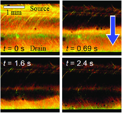
Anisotropic carrier transport in organic luminescent polymer semiconductor thin film is directly visualized using real-time photoluminescence (PL) decay imaging. Difference in the mobility anisotropy for hole and electron is clearly observed. That is attributed to the difference in the electron distribution in the highest occupied molecular orbital (HOMO) and lowest unoccupied molecular orbital (LUMO) levels.
Ni-Based Coordination Polymer as a Promising Anode Material for Potassium Batteries
- First Published: 15 May 2020
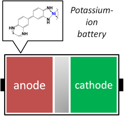
Ni-based 1D coordination polymer Ni-DAB derived from 3,3′-diaminobenzidine ligand is shown to be a stable and fast anode material for potassium batteries operating in the safe voltage window of 0.4–2.0 V versus K+/K. Capacity of 158 mA h g−1 is delivered by Ni-DAB at 1 A g−1, whereas the capacity fade is only 8.6% after 600 cycles.
Controlled Growth of Vertically Oriented Trilayer MoS2 Nanoflakes for Room-Temperature NO2 Gas Sensor Applications
- First Published: 21 April 2020
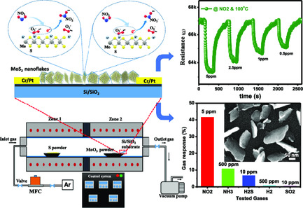
Without the use of any buffer layer, vertically oriented trilayer MoS2 nanoflakes are grown on-chip by chemical vapor deposition method for room-temperature NO2 gas sensor application. Taking advantages of the vertically aligned nanoflakes, the NO2 gas is adsorbed on both sides of the nanoflakes, thus significantly enhancing the gas sensing performance of the sensor.
Functionalized Naphthalene Diimides as Low-Cost Organic Cathodes for Potassium Batteries
- First Published: 15 May 2020
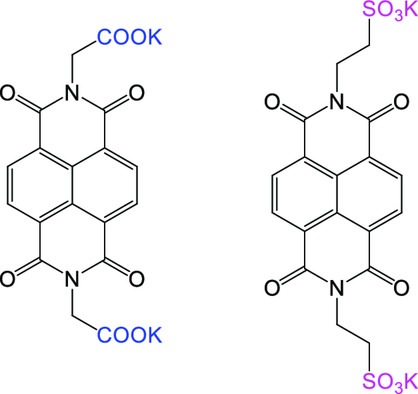
Two simple redox-active naphthalene diimide derivatives bearing sulfonic and carboxylic groups in the form of potassium salts are synthesized. Promising specific capacity of 86–96 mAh g−1 in combination with average cell discharge potentials of ≈2.2 V is achieved, thus featuring these compounds as cheap and scalable cathode materials for potassium batteries designed for stationary energy storage applications.
Sign up for email alerts
Tools
![]()
In 2022, the youngest family member physica status solidi (RRL) – Rapid Research Letters is turning 15 years. To celebrate this milestone, we present a new virtual collection with invited articles.
![]()
As we celebrate the 60th anniversary year of the physica status solidi family, click here to access our continuously updated collection of invited articles written by authors and partners of the pss journals.