
Journal list menu

 Issue
Issuephysica status solidi (RRL) – Rapid Research Letters: Volume 18, Issue 7
Special Issue: Recent Advances in Semiconductor Materials and Devices
July 2024Guest Editor(s):
Export Citations
Download PDFs
Cover Picture
Understanding the Breakdown Behavior of Ultrawide-Bandgap Boron Nitride Power Diodes Using Device Modeling
- First Published: 18 July 2024

Ultrawide-Bandgap Boron Nitride Power Diodes
In article number 2200397, Yuji Zhao and co-workers report on a device study using technology computer-aided design simulation to theoretically analyze the electrical performance of ultrawide bandgap boron-nitride (BN)-based vertical junction devices, including hexagonal (h)-BN Schottky diode, h-BN p–n diode, and h-BN/AlN p–n diode. The BN devices show outstanding performance and a high potential for future power electronic devices. The critical electric field of 2 × 1016 cm−3 p-type-doped h-BN is calculated to be 13.6 MV/cm.
Inside Front Cover
Solar-Blind Deep-Ultraviolet Photoconductive Detector Based on Amorphous Ga2O3 Thin Films for Corona Discharge Detection
- First Published: 18 July 2024
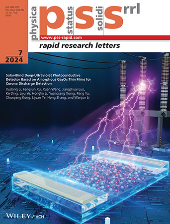
Fully-Transparent Solar-Blind Photodetector
In article number 2200512, Lijuan Ye, Hong Zhang, Wanjun Li, and co-workers propose a strategy to construct a fully transparent and high-performance solar-blind photoconductive detector based on amorphous Ga2O3 film, which effectively detects extremely weak solar-blind deep-ultraviolet signals through simulated corona discharge detection.
Masthead
Guest Editorial
Recent Advances in Semiconductor Materials and Devices
- First Published: 18 July 2024
Review
A Review of Intercalation of Rare Gas Solids on Graphene and Hexagonal Boron Nitride
- First Published: 10 June 2023
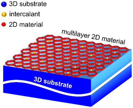
Herein, the emerging field of research focuses on the intercalation of rare gas solids on graphene and hexagonal boron nitride to generate novel intercalated systems. Despite the availability of a few experimental studies on this topic, vast research and niche application opportunities still exist in this nascent and rapidly growing field.
Research Article
Ultrasmall CoSe2 Nanoparticles Grown on MoS2 Nanofilms: A New Catalyst for Hydrogen Evolution Reaction
- First Published: 01 August 2023
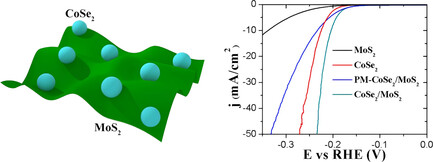
Ultrasmall CoSe2 nanoparticles are successfully grown on MoS2 nanofilms using a facile and low-cost hydrothermal method. With the small Tafel slope (37.8 mV dec−1) and low overpotential, the CoSe2/MoS2 hybrid catalyst shows good hydrogen evolution reaction activity. In addition, the CoSe2/MoS2 catalyst exhibits long-term durability under acidic conditions as well.
Structural, Electronic, Optical, and Mechanical Properties of Cu(I)Au(III)-Based Double Perovskites: A First-Principles Study
- First Published: 25 May 2023
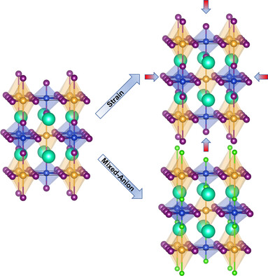
There are many researches on Ag-based and Au-based halide perovskites, but few on CuAu-based ones. Herein, the authors investigate the effect of mixed anions and strain on the compounds and find some interesting results, mainly resulting from the Jahn–Teller effect in CuAu-based double halide perovskites.
Theoretical Insights into Photovoltaic Application of a Novel Family of Perovskite-Inspired Pb-Free Metal Halide Materials
- First Published: 24 May 2023
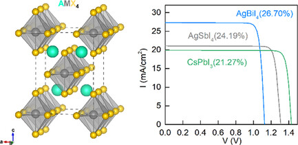
The optoelectronic properties of a series of novel Pb-free perovskite-like materials AMX4 (A = Cs, Ag and Rb; M = In, Sb and Bi; X = Cl, Br and I) are investigated by first-principles calculations, and their device performances are further simulated by the SCAPS code, which exhibit promising potential in the photovoltaic application.
Colloidal Quantum Dots-Based Three-Band Infrared Photodetector with the Bias-Tunable Spectral Response
- First Published: 24 May 2023
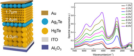
A colloidal quantum dot-based three-band infrared detector with short-wave infrared of 1.7 and 2.4 μm and midwave infrared of 4 μm controlled by the bias voltage with spatially stable doping of Ag2Te nanocrystals is studied.
Synthesis of Nonlayered 2D α-Fe2O3 Nanosheets by Ultralow Concentration Precursor with Se Catalysts Design
- First Published: 25 April 2023
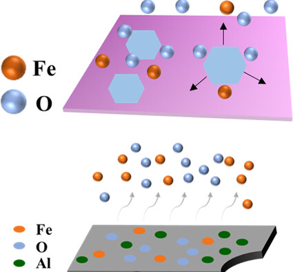
A new growth strategy is created by designing ultralow concentration precursors and Se catalysts, achieving the ultrathin α-Fe2O3 2D nanosheets with single-crystalline quality and large lateral size after tuning the growth temperature. The reasonable photoconductive response performance is shown by α-Fe2O3 photodetectors. Herein, a special growth technique for the synthesis of ultrathin 2D nonlayered materials is provided.
Solar-Blind Deep-Ultraviolet Photoconductive Detector Based on Amorphous Ga2O3 Thin Films for Corona Discharge Detection
- First Published: 09 February 2023
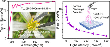
A fully transparent solar-blind deep-ultraviolet photoconductive detector with transparent electrodes is successfully constructed based on amorphous Ga2O3 films. The device demonstrates an ultra-high responsivity of 1.3 × 10⁴ A W−1, a detectivity of 3.2 × 10¹⁴ Jones, and an external quantum efficiency of 6.7 × 10⁶%. Also, the fully transparent device is applied to a proof-of-concept of high-voltage corona system to achieve solar-blind signal detection.
Lattice-Asymmetry-Driven Selective Area Sublimation: A Promising Strategy for III-Nitride Nanostructure Tailoring
- First Published: 19 April 2023
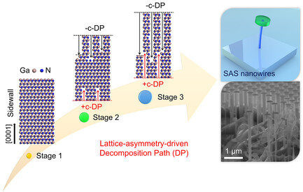
The rationale of the selective area sublimation (SAS) is confirmed as a strong anisotropic decomposition driven by lattice-asymmetry of wurtzite crystal: the sublimation preferably starts along the -c axis due to the relatively lower decomposition energy barrier. The fabrication of site- and size-controlled GaN nanowires has been achieved by utilizing the SAS process, exhibiting good controllability on the sidewall of nanowires.
Understanding the Breakdown Behavior of Ultrawide-Bandgap Boron Nitride Power Diodes Using Device Modeling
- First Published: 03 January 2023
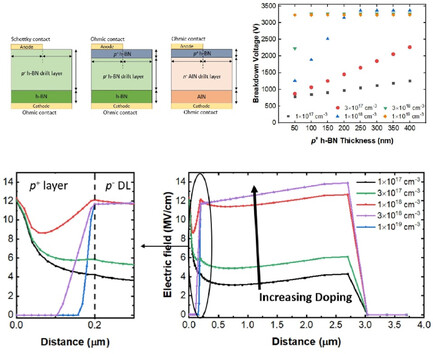
A device study using technology computer-aided design simulation is performed to theoretically analyze electrical performance of ultrawide-bandgap boron nitride (BN)-based vertical junction devices, including h-BN Schottky diode, h-BN pn diode, and h-BN/AlN pn diode, which provides an understanding of the device principles of vertical BN junctions, which can serve as a reference for the future development of BN power electronics.
Structure-Induced Tunable Multipolar Moments and the Associated Purcell Enhancement in Silicon-Like Metasurfaces
- First Published: 24 December 2022
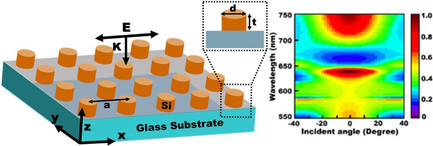
An all-dielectric metasurface with tunable Kerker condition to enhance emission from single nitrogen-vacancy center at zero-phonon line (ZPL) wavelength of 640 nm is discussed. The coherent superposition of multipolar moments results in Kerker condition, which depends on structural parameters of metasurfaces. Purcell enhancement of 300 times is achieved at ZPL, which is tunable by changing Kerker condition.
Ultranarrow Band UV Detection in GaN with Simple Device Architecture
- First Published: 08 November 2022
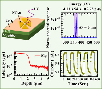
An ultranarrow-band ultraviolet (UV) GaN detector based on a simple p-GaN/un-intentionally doped GaN epilayer is presented. The device response is centred at 366 nm with only ≈5 nm width and UV–vis rejection ratio of >2 × 10³. The results demonstrate an innovative methodology for achieving a stable and high spectrum-selective UV photodetection without involving complex device architecture.
Metal–Organic Vapor-Phase Epitaxy of Semipolar InGaN Quantum Dots Based on GaN V-Shaped Pits
- First Published: 17 September 2022
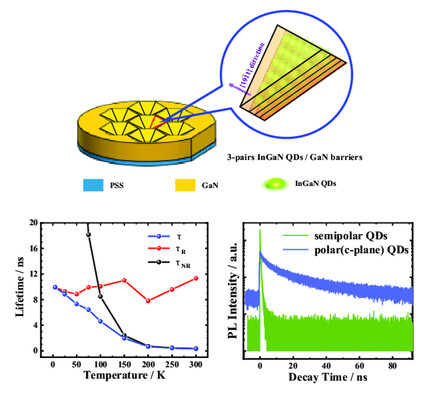
A novel method to fabricate semipolar InGaN quantum dots (QDs) by metal–organic vapor phase epitaxy is reported. The ellipse-shaped semipolar InGaN QDs with 523 nm photoluminescence emission at room temperature are formed on the GaN V-shaped pits directly grown on c-plane patterned sapphire substrate.
Enhanced Resonant Energy Transfer by Decorating Au Nanoparticles on the Sidewalls of InGaN Multiple-Quantum-Well Nanorods
- First Published: 10 June 2022
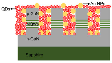
Herein, different heights of InGaN multiple quantum well (MQW) nanorods are fabricated and decorated with Au nanoparticles. The Au nanoparticles were found to be able to enhance the resonant energy transfer (RET) process between InGaN MQWs and quantum dots. The high RET efficiency in the hybrid structure demonstrated high potential for usage in energy conversion devices.
Structure and Electronic Properties of 2D GaN/AlxGa1−xN 2D/3D Heterostructure Controlled by Al Components and Interlayer Distance
- First Published: 29 June 2022
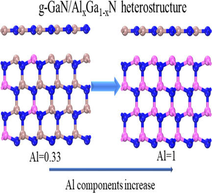
Herein, atomic structure and electronic properties of g-GaN/AlxGa1−xN heterostructure with different Al components and interlayer distance are discussed. Ordered arrangement of Al components in AlxGa1−xN materials is more conducive to forming heterostructures. The g-GaN/Al0.5Ga0.5N heterostructure is most stable by comparing binding energy under different Al components. The optimal interlayer distance range of heterostructure is 2.5–3 Å.
Sign up for email alerts
Tools
![]()
In 2022, the youngest family member physica status solidi (RRL) – Rapid Research Letters is turning 15 years. To celebrate this milestone, we present a new virtual collection with invited articles.
![]()
As we celebrate the 60th anniversary year of the physica status solidi family, click here to access our continuously updated collection of invited articles written by authors and partners of the pss journals.