
Journal list menu

 Issue
Issuephysica status solidi (RRL) – Rapid Research Letters: Volume 16, Issue 1
January 2022
Export Citations
Download PDFs
Cover Picture
Solid-Phase Crystallization of GeSn Thin Films on GeO2-Coated Glass
- First Published: 06 January 2022
In article number 2100509, Kaoru Toko and co-workers illustrate how oxygen diffusion from the GeO2 layer during crystallization enables the synthesis of GeSn layers with large grains, which considerably reduces acceptor defects while maintaining a high hole mobility. These achievements will pave the way for advanced Ge-based thin-film transistors.
Masthead
Editorials
More Milestones: 15 Years of physica status solidi (RRL) – Rapid Research Letters
- First Published: 06 January 2022
Reviews
15 years of pss RRL
Chemical Vapor Deposition Single-Crystal Diamond: A Review
- First Published: 17 September 2021
Single-crystal diamond is the material of choice for future power electronics and quantum devices. The state of the art of single-crystal diamond growth by chemical vapor deposition, either starting with a diamond substrate (homoepitaxy) or controlling diamond nucleation on a foreign substrate (heteroepitaxy) is described. Future challenges and roles of both materials in the applications are discussed.
Recent Progress and Perspectives of Field-Effect Transistors Based on p-Type Oxide Semiconductors
- First Published: 21 September 2021
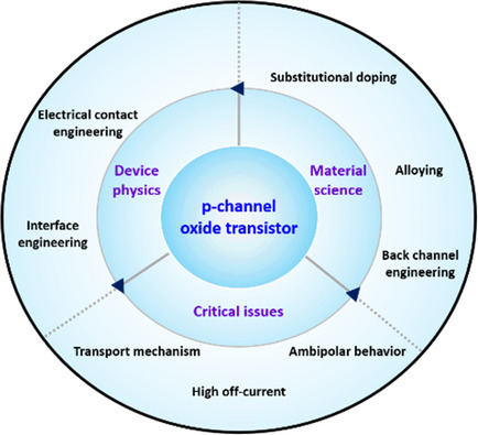
A brief history, recent achievements, and future directions for p-channel oxide field-effect transistors are addressed. The representative p-type oxide semiconductors based on copper and tin are reviewed. The studies reviewed adopted complementary metal–oxide–semiconductor (CMOS)-compatible fabrication methods, such as physical or chemical vapor deposition.
Research Articles
15 years of pss RRL
Partial Auxeticity of Laterally Compressed Carbon Nanotube Bundles
- First Published: 12 September 2021
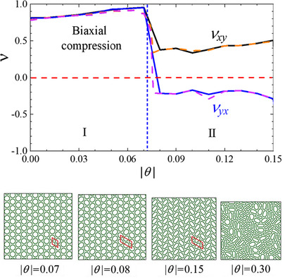
A bundle of carbon nanotubes (CNTs) exhibits unusual elastic properties under biaxial compression. With increasing compressive strain, the Poisson's ratios of the bundle approach 1 before the CNTs lose their circular shape. After the bundle loses the cross-sectional isotropy due to the CNT shape change, one of its Poisson's ratios becomes negative.
Low-Temperature Growth of Au-Catalyzed InAs Nanowires: Experiment and Theory
- First Published: 21 September 2021
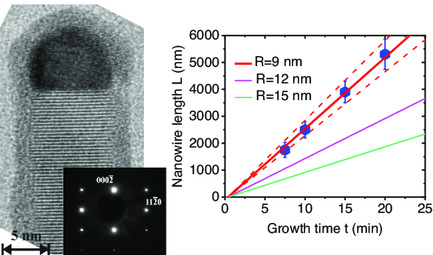
Unusually high axial growth rate (4.4 nm s−1) of Au-catalyzed InAs nanowires (NWs) grown by molecular beam epitaxy (MBE) on silicon at 270 °C is revealed. Surprisingly, the low temperature leads to a considerable enhancement of the NW growth rate compared to the vapor–liquid–solid (VLS) growth despite the catalyst nanoparticle being solid.
Hierarchically Interlaced 2D Copper Iodide/MXene Composite for High Thermoelectric Performance
- First Published: 01 September 2021
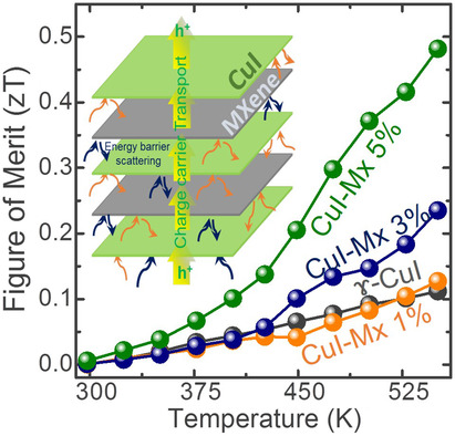
Layered 2D thermoelectric materials are known for their exceptional electrical and thermal properties. Hierarchical structuring of these novel 2D materials enhances the thermoelectric properties by steadily tuning the electron and phonon transport characteristics in the material. In this work, the phenomenon of interfacial energy barrier scattering in the hierarchically interlaced structure of copper iodide with Mxene for enhanced thermoelectric performance is demonstrated.
Impact of Substrate Hydrophobicity on Layer Composition and Work Function of PEDOT:PSS Thin Films
- First Published: 19 October 2021
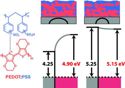
The work function of spin-coated PEDOT:PSS thin films on O2–plasma- or UV–ozone-treated indium tin oxide is around 5 eV and rather independent of the substrate cleaning parameters. Moreover, the PEDOT:PSS layer thickness does not affect the work function. Increasing the substrate hydrophobicity by self-assembled monolayers provides a facile way to increase the PEDOT:PSS work function up to 5.15 eV.
Large Anharmonicity and Low Lattice Thermal Conductivity of Thermoelectric Sn(SbTe2)2
- First Published: 06 October 2021
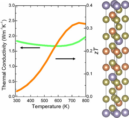
Sn(SbTe2)2 is considered as a promising thermoelectric material with a relatively high zTmax of 0.32 at 770 K, mainly due to its extremely low lattice thermal conductivity. It is experimentally confirmed that such low thermal conductivity is related to a strong anharmonicity in the material, indicated by its relatively high Grüneisen parameter.
Thin-Film Solar Cells of an Indium-Modified Silver Antimony Sulfide Selenide Absorber Prepared by Spray Pyrolysis
- First Published: 09 September 2021
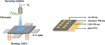
Spray pyrolysis is used to fabricate a film with In-added Ag–Sb–S and the film is selenized subsequently. With the addition of In, the morphology and the crystallinity of the films are simultaneously improved due to the diminished defects. The power conversion efficiency of the device is largely improved from 0.74% (In/Sb = 0) to 1.98% (In/Sb = 0.47).
Editor's Choice
Preferential Placement of Aligned Nitrogen Vacancy Centers in Chemical Vapor Deposition Overgrown Diamond Microstructures
- First Published: 09 September 2021
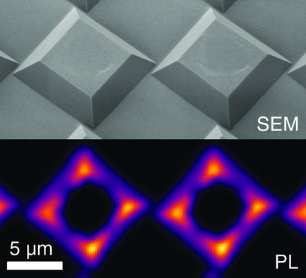
Nitrogen vacancy (NV) centers are selectively placed on a diamond substrate with their crystallographic axes aligned to enhance fluorescence contrast. This is achieved by nitrogen-doped chemical vapor deposition (CVD) overgrowth of dry chemically etched diamond structures. The resulting NV centers exhibit long spin coherence times and minimal residual spin noise is detected in the host diamond crystal.
Magnetoelectric Switching Energy of Antiferromagnetic Cr2O3 Used for Spintronic Logic Devices and Memory
- First Published: 01 September 2021
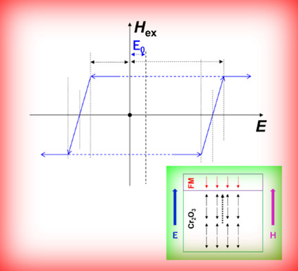
Antiferromagnetic oxide Cr2O3-based perpendicular exchange-coupling heterostructures are promising for use in spintronic logic devices and memory. However, the magnetoelectric (ME) switching energy, which is the most crucial aspect of these systems, remains unclear. In this work, a phenomenological model based on literature data is developed to clarify this item, and the asymmetric ME switching behavior of Cr2O3 is also explored.
Magnetic and Critical Properties of Cr1/3NbS1.86 with T C = 56 K
- First Published: 22 September 2021
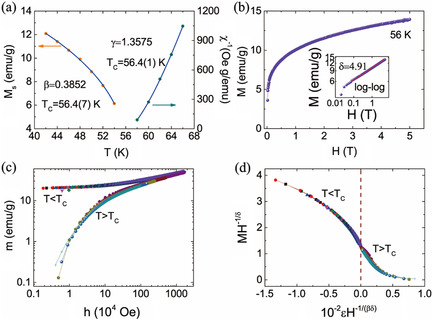
Cr1/3NbS2 triggers intensive interest as it provides a unique opportunity to study simultaneously the interplay of reduced dimensionality, crystallographic/magnetic chirality, and topologically magnetic order novelty. In this work, the magnetic and critical behavior of a low-Curie-temperature single crystal is demonstrated. The properties are elucidated by the magnetic measurements and the scaling law analysis.
Phase Diagram of Sub-GHz Electric-Field-Induced Polarization Oscillation
- First Published: 24 September 2021
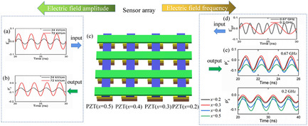
Through applying sub-GHz electric field external stimuli, in Pb(Zr,Ti)O3, the maximum polarization and strain oscillation amplitude can be obtained through the frequency tuning of the input ac electric field. The maximum polarization behavior occurs at the point that the phase difference between the input electric field and the polarization response is π/2.
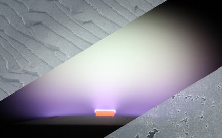
High Hole Mobility of Polycrystalline GeSn Layers Grown by Hot-Wire Chemical Vapor Deposition on Diamond Substrates
- First Published: 28 September 2021
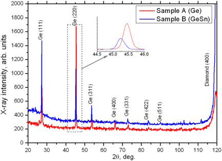
The conditions for the growth of polycrystalline GeSn layers by the hot-wire chemical vapor deposition method at 300 °C without annealing on diamond substrates are determined. It is shown that the incorporation of 1% Sn into the Ge lattice significantly increases the hole mobility of GeSn layers from 30 to 140 cm2 V−1 s−1.
Local Structure of Ga85:8In14:2 Eutectic Alloy and Its Pressure–Temperature Melting Line
- First Published: 01 October 2021
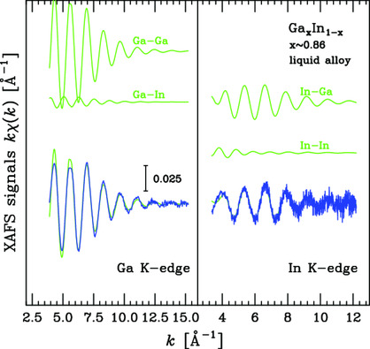
The local structures in the Ga85.8In14.2 eutectic liquid alloy at ambient conditions are analyzed with details using double-edge refinements of the X-ray absorption fine structure (XAFS). The pressure–temperature melting line of the alloy is established up to 10 GPa using combined X-ray absorption and diffraction measurements.
Electrically Pumped Epitaxially Regrown GaSb-Based Type-I Quantum-Well Surface-Emitting Lasers with Buried High-Index-Contrast Photonic Crystal Layer
- First Published: 25 September 2021
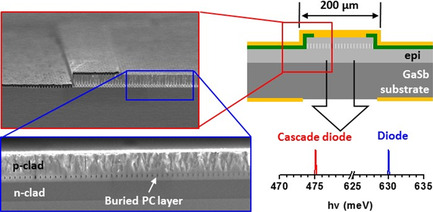
GaSb-based photonic crystal surface-emitting lasers operating near 2 and 2.6 μm are designed, fabricated, and characterized. A high-index-contrast photonic crystal layer is incorporated into the diode and cascade diode laser heterostructure by air-hole-retaining epitaxial regrowth. The devices generate mW-level output in a narrow divergence beam emitted from the window in the substrate contact.
Second-Harmonic Generation Based on the Dual-Band Second-Order Topological Corner States
- First Published: 21 September 2021
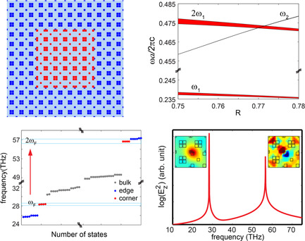
Efficient second-harmonic generation (SHG) using dual-band second-order topological corner states is reported. Dual-band corner states can be obtained in the first and second bandgaps, when the eigenfrequency of the corner state in the higher bandgap is twice that of corner one in the lower gap, resulting on high SHG efficiency in the order of 10−1%.
Potassium versus Sodium in Cu(In,Ga)Se2—Similarities and Differences in the Electrical Characteristics of Solar Cells and Thin Films after NaF or KF Postdeposition Treatment
- First Published: 05 October 2021
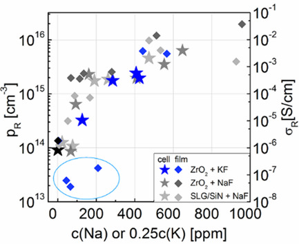
Thermal equilibrium and metastable (after light soaking) electrical properties of Cu(In,Ga)Se2 thin films (conductivity) and corresponding solar cells (hole concentration) are investigated after doping with a controlled amount of sodium or potassium. Similarities in the impact of both alkali metals point to the changes not being atom-specific and being likely caused by grain boundary passivation.
Electro−Photo Double Control of Resistive Switching in Electron-Doped La0.9Hf0.1MnO3 Films
- First Published: 14 October 2021
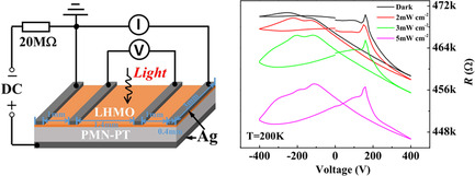
Light and electric field double control of electronic transport in electron-doped manganite films on ferroelectric crystals is demonstrated. The photoresistance effect and the electroresistance effect highly correlate with each other. The relative magnitude of the electric-field-induced lattice strain effect and interfacial charge effect is identified to be controllable by applying light and by not just varying temperature.
Strong Electron–Phonon Coupling in 3D WN and Coexistence of Intrinsic Superconductivity and Topological Nodal Line in Its 2D Limit
- First Published: 06 October 2021
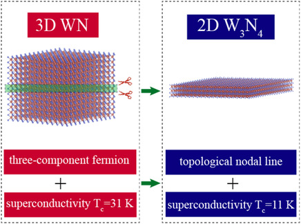
The three-component-fermion candidate WN behaves as a good superconductor with Tc of 31 K. The WN thin film is also predicted to be an intrinsic superconductor with Tc of 11 K; it hosts nodal lines that are robust against spin–orbit coupling (SOC), close to the Fermi level and apart from other trivial bands, which are scarce in real materials.
15 years of pss RRL
Solid-Phase Crystallization of GeSn Thin Films on GeO2-Coated Glass
- First Published: 06 November 2021
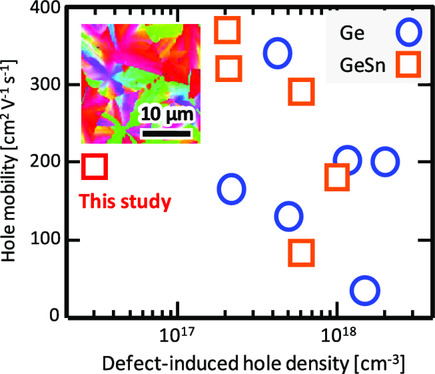
Sn addition and GeO2 preparation considerably lower the density of acceptor defects in polycrystalline Ge layers. The GeSn layer formed by low-temperature (375 °C) solid-phase crystallization records a low hole concentration (3 × 1016 cm−3) while maintaining a high hole mobility (190 cm2 V−1 s−1) owing to the large grain size (15 μm diameter).
Sign up for email alerts
Tools
![]()
In 2022, the youngest family member physica status solidi (RRL) – Rapid Research Letters is turning 15 years. To celebrate this milestone, we present a new virtual collection with invited articles.
![]()
As we celebrate the 60th anniversary year of the physica status solidi family, click here to access our continuously updated collection of invited articles written by authors and partners of the pss journals.