

Journal list menu

 Issue
Issuephysica status solidi c: Volume 9, Issue 3-4
Special Issue:9th International Conference on Nitride Semiconductors (ICNS‐9); see further papers in Phys. Status Solidi B 249, No. 3 (2012) and Phys. Status Solidi A 209, No. 3 (2012) • E‐MRS 2011 Spring Meeting – Symposium H; see further papers in Phys. Status Solidi A 209, No. 1 (2012) • E‐MRS 2011 Spring Meeting – Symposium F; see further papers in Phys. Status Solidi RRL 6, No. 2 (2012) and Phys. Status Solidi B 249, No. 3 (2012)
411-1113March 2012
Export Citations
Download PDFs
Cover Picture
Cover Picture: Phys. Status Solidi C 3–4/2012
- First Published: 22 March 2012
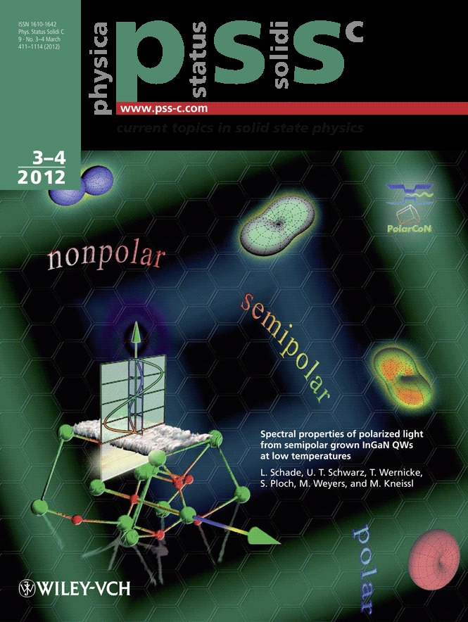
In the nitride system, polarization of light is an extraordinary property of quantum wells (QWs) with growth direction inclined to the c-axis. This anisotropy of emission is a direct consequence of strain symmetry in these pseudomorphically grown semipolar and nonpolar oriented layers.
A nonpolar quantum well above a schematic illustration of the wurtzite crystalline structure is drafted in the left part of the image. This property of its emission is expressed by spherical harmonics on top. They reflect the optical polarization of the emitted light in all growth directions. From polar to nonpolar grown QWs, even a switching behavior can be detected, indicated on the surrounding circle.
In their article on pp. 700 L. Schade et al. report on the spectral properties of optically polarized light originating from semipolar and nonpolar InGaN quantum wells at low temperatures. There, only one radiative transition contributes to the emission. All data can be explained by the influence of the varying indium content within the quantum wells of different crystal orientation.
Back Cover
Back Cover: Phys. Status Solidi C 3–4/2012
- First Published: 22 March 2012
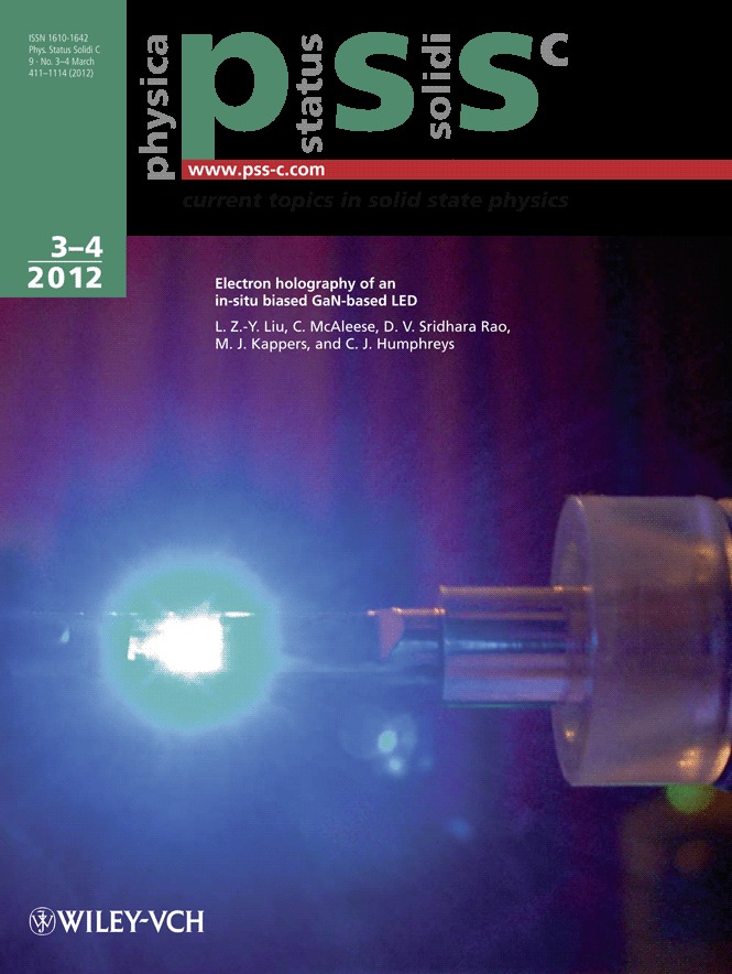
The work of Lewis Z.-Y. Liu et al. (pp. 704) enables high resolution real-time characterisation of LEDs under their working conditions. The figure shows a GaN-based LED chip emitting light on an in-situ biasing TEM holder, on which a TEM lamella has been prepared by FIB. The design ensures that a significant amount of the current goes through the cross-sectional TEM lamella. The paper focuses on using electron holography to determine the electrostatic potential across the LED structure. This experimental platform allows a variety of TEM techniques to be applied to extract a range of information from a working LED at high spatial resolution.
Issue Information
Contents
Contents: Phys. Status Solidi C 3–4/2012
- Pages: 411-427
- First Published: 22 March 2012
ICNS-9 – Preface
Preface: Phys. Status Solidi C 3–4/2012
- Pages: 430-432
- First Published: 22 March 2012
ICNS-9 – Contributed Articles
Bulk and template growth
Atomically controlled chemical polishing of GaN using platinum and hydrofluoric acid
- Pages: 433-435
- First Published: 29 February 2012
In situ monitoring technologies for ammonthermal reactors
- Pages: 436-439
- First Published: 21 November 2011
Epitaxial lateral overgrowth of InGaN/GaN multiple quantum wells on HVPE GaN template
- Pages: 445-448
- First Published: 07 December 2011
Faceting in AlN bulk crystal growth and its impact on optical properties of the crystals
- Pages: 449-452
- First Published: 13 January 2012
High nitrogen pressure solution growth of GaN in multi feed-seed configuration
- Pages: 453-456
- First Published: 03 February 2012
Effect of additives on liquid phase epitaxy growth of non-polar GaN single crystals using Na flux method
- Pages: 457-460
- First Published: 24 November 2011
Epitaxial growth and structural properties
The negligible effects of miscut on indium aluminium nitride growth
- Pages: 461-464
- First Published: 29 November 2011
On the origin of blue-green emission from heteroepitaxial nonpolar a-plane InGaN quantum wells
- Pages: 465-468
- First Published: 26 January 2012
Transfer characteristic of zinc nitride based thin film transistors
- Pages: 469-472
- First Published: 29 February 2012
Improved surface morphology and mobility of AlGaN/GaN HEMT grown on silicon substrate
- Pages: 473-475
- First Published: 29 November 2011
Monolithic integration of semipolar pyramidal LEDs with tailored wavelengths
- Pages: 476-479
- First Published: 29 November 2011
In-situ void formation technique using an AlN shell structure grown on GaN stripes on Si(111) and c-plane sapphire substrates
- Pages: 480-483
- First Published: 26 January 2012
Effect of doping on screw threading dislocations in AlN and their role as conductive nanowires
- Pages: 484-487
- First Published: 29 February 2012
Behavior of misfit dislocations in semipolar InGaN/GaN grown by MOVPE
- Pages: 488-491
- First Published: 07 December 2011
Investigations on Si-doped AlGaN: Below and above the Mott density
- Pages: 492-495
- First Published: 26 January 2012
Investigation of inversion domain formation in AlN grown on sapphire by MOVPE
- Pages: 496-498
- First Published: 12 December 2011
Effects of carrier gas ratio and growth temperature on MOVPE growth of AlN
- Pages: 499-502
- First Published: 26 January 2012
Epitaxial growth of GaN films on Si(110) substrates by rf-MBE
- Pages: 503-506
- First Published: 24 November 2011
Growth and stacking fault reduction in semi-polar GaN films on planar Si(112) and Si(113)
- Pages: 507-510
- First Published: 26 January 2012
Significance of initial stages on the epitaxial growth of AlN using high temperature halide chemical vapor deposition
- Pages: 511-514
- First Published: 24 November 2011
Influence of sputter power and N2 gas flow ratio on crystalline quality of AlN layers deposited at 823 K by RF reactive sputtering
- Pages: 515-518
- First Published: 12 December 2011
Growth of GaN and AlGaN on (100) β-Ga2O3 substrates
- Pages: 519-522
- First Published: 26 January 2012
Influence of nitrogen precursor and its flow rate on the quality and the residual doping in GaN grown by molecular beam epitaxy
- Pages: 523-526
- First Published: 26 January 2012
Formation of low-resistance and thermally stable Ohmic contacts to laser lift-off prepared N-polar n-GaN
- Pages: 527-529
- First Published: 07 December 2011
Anion modulation epitaxy (AME), an alternative growth strategy for group III-nitrides
- Pages: 530-533
- First Published: 03 February 2012
Structural characterization of InN epilayers grown on r -plane sapphire by plasma-assisted MBE
- Pages: 534-537
- First Published: 14 February 2012
Plasma-assisted electroepitaxy as a novel method for the growth of GaN layers
- Pages: 538-541
- First Published: 03 February 2012
MOVPE growth of InGaAsN films on Ge(001) on-axis and vicinal substrates
- Pages: 542-545
- First Published: 07 December 2011
Characterization of InGaN/GaN epitaxial layers by aberration corrected TEM/STEM
- Pages: 546-549
- First Published: 26 January 2012
Strain control of GaN grown on 3C-SiC/Si substrate using AlGaN buffer layer
- Pages: 550-553
- First Published: 24 November 2011
III-nitride grown on freestanding GaN nanostructures
- Pages: 554-557
- First Published: 29 February 2012
MBE growth of cubic AlN films on MgO substrate via cubic GaN buffer layer
- Pages: 558-561
- First Published: 29 February 2012
Growth of high quality III-N heterostructures using specialized MBE system
- Pages: 562-563
- First Published: 15 February 2012
Greatly improved crystal quality of non-polar GaN grown on a-plane GaN nano-rod template obtained using self-organised nano-masks
- Pages: 564-567
- First Published: 26 January 2012
Growth of {11-22} GaN on shallowly etched r -plane patterned sapphire substrates
- Pages: 568-571
- First Published: 24 November 2011
Improved crystalline quality and light output power of GaN-based light-emitting diodes grown on Si substrate by buffer optimization
- Pages: 572-575
- First Published: 26 January 2012
Fabrication of crack-free thick AlN film on a-plane sapphire by low-pressure HVPE
- Pages: 576-579
- First Published: 29 February 2012
The role of liquid phase epitaxy during growth of AlGaN by MBE
- Pages: 580-583
- First Published: 07 December 2011
Schottky barrier and interface chemistry for Ni contacted to Al0.8Ga0.2N grown on c-oriented AlN single crystal substrates
- Pages: 584-587
- First Published: 26 January 2012
Sequential tunneling transport in GaN/AlGaN quantum cascade structures
- Pages: 588-591
- First Published: 26 January 2012
Optimization of AlGaN-based spacer layer for InAlN/GaN interfaces
- Pages: 592-595
- First Published: 12 December 2011
Nanostructures and novel nitride alloys
Self-catalyzed, vertically aligned GaN rod-structures by metal-organic vapor phase epitaxy
- Pages: 596-600
- First Published: 29 November 2011
InGaN/GaN quantum wells grown on freestanding HfO2 photonic crystals
- Pages: 601-604
- First Published: 13 January 2012
Epitaxial growth and properties of GdN, EuN and SmN thin films
- Pages: 605-608
- First Published: 07 December 2011
Fabrication of site-controlled InGaN quantum dots using reactive-ion etching
- Pages: 609-612
- First Published: 07 December 2011
Self-assembled m -plane InGaN quantum dots: formation and shape evolution
- Pages: 613-615
- First Published: 26 January 2012
Size effect on efficiency droop of blue light emitting diode
- Pages: 616-619
- First Published: 12 December 2011
Investigation of the optical properties of InGaN/GaN nanorods with different indium composition
- Pages: 620-623
- First Published: 26 January 2012
Morphology evolution and optical properties of GaN nano-pyramids grown by selective area MOVPE
- Pages: 624-627
- First Published: 21 November 2011
X-ray excited optical luminescence imaging of InGaN nano-LEDs
- Pages: 628-630
- First Published: 21 November 2011
Fabrication and properties of etched GaN nanorods
- Pages: 631-634
- First Published: 21 November 2011
Optical studies of quantum dot-like emission from localisation centres in InGaN/GaN nanorod array LEDs
- Pages: 635-638
- First Published: 03 February 2012
Characterization of single semiconductor nanowires by synchrotron radiation nanoprobe
- Pages: 639-641
- First Published: 14 February 2012
Responsivity and photocurrent dynamics in single GaN nanowires
- Pages: 642-645
- First Published: 13 January 2012
Growth of InGaN nanowires on a (111)Si substrate by RF-MBE
- Pages: 646-649
- First Published: 26 January 2012
InN and related materials
Growth of crack-free GaN epitaxial thin films on composite Si(111)/polycrystalline diamond substrates by MOVPE
- Pages: 650-653
- First Published: 14 February 2012
Phase diagram on phase purity of InN grown pressurized-reactor MOVPE
- Pages: 654-657
- First Published: 03 February 2012
RF-MBE growth of semipolar InN(10-13) and InGaN(10-13) on GaAs(110)
- Pages: 658-661
- First Published: 29 February 2012
Surface electronic properties of In-rich InGaN alloys grown by MOCVD
- Pages: 662-665
- First Published: 07 December 2011
Growth of InN quantum dots by droplet epitaxy and their characterization
- Pages: 666-669
- First Published: 12 December 2011
MOVPE growth of InGaN on Si(111) substrates with an intermediate range of In content
- Pages: 670-672
- First Published: 24 November 2011
Anti-corrosive stainless steel separator coated with MOCVD InGaN for polymer electrolyte fuel cell (PEFC)
- Pages: 673-676
- First Published: 03 February 2012
Influence of growth temperature on the twin formation of InN{10 3} on GaAs(110) by metalorganic vapor phase epitaxy
- Pages: 677-680
- First Published: 21 November 2011
Relationship between residual carrier density and phase purity in InN grown by pressurized-reactor MOVPE
- Pages: 681-684
- First Published: 26 January 2012
Valence band offsets at oxide/InN interfaces determined by X-ray photoelectron spectroscopy
- Pages: 685-688
- First Published: 13 January 2012
Peculiarities of galvanomagnetic effects in GaN epilayers and GaN/InGaN quantum wells
- Pages: 689-692
- First Published: 29 February 2012
Surface photovoltage spectroscopy characterization of Al1-xInxN/AlN/GaN heterostructures
- Pages: 693-696
- First Published: 24 November 2011
Highly enhanced migration in Pt-catalyst-assisted MOVPE InN by controlling the catalyst temperature
- Pages: 697-699
- First Published: 26 January 2012
Optical and magnetic properties
Spectral properties of polarized light from semipolar grown InGaN quantum wells at low temperatures
- Pages: 700-703
- First Published: 29 November 2011
Electron holography of an in-situ biased GaN-based LED
- Pages: 704-707
- First Published: 26 January 2012
Injection efficiency and optical gain characteristics of polar and nonpolar III-nitride light emitters
- Pages: 708-711
- First Published: 07 December 2011
Optical studies of GaN nanocolumns containing InGaN quantum disks and the effect of strain relaxation on the carrier distribution
- Pages: 712-714
- First Published: 13 January 2012
Photoluminescence changes in n-type GaN samples after photoelectrochemical treatment
- Pages: 715-718
- First Published: 29 February 2012
Large magneto-optical effect in low-temperature-grown GaCrN and GaCrN:Si
- Pages: 719-722
- First Published: 12 December 2011
Effect of GaN cap thickness on carrier dynamics in InGaN quantum wells
- Pages: 727-729
- First Published: 21 November 2011
Observation of A1(LO), E2(high) and B1(high) phonon modes in Inx Ga1–xN alloys with x = 0.11–0.54
- Pages: 730-732
- First Published: 12 December 2011
Photoluminescence properties of Al-rich AlXGa1-XN grown on AlN/sapphire template by MOCVD
- Pages: 733-736
- First Published: 26 January 2012
Structural, magnetic and optical studies of ultrathin GaGdN/AlGaN multiquantum well structure
- Pages: 737-740
- First Published: 12 December 2011
Effect of growth conditions on magnetic and structural properties in Gd-doped GaN layers grown by plasma-assisted molecular beam epitaxy
- Pages: 741-744
- First Published: 21 November 2011
Shallow donors and deep level color centers in AlN single crystals: EPR, ODMR and optical studies
- Pages: 745-748
- First Published: 21 November 2011
Light emitting diodes and improving efficiency
Highly-uniform 260 nm-band AlGaN-based deep-ultraviolet light-emitting diodes developed by 2-inch×3 MOVPE system
- Pages: 749-752
- First Published: 07 December 2011
Laser lift-off of AlN/sapphire for UV light-emitting diodes
- Pages: 753-756
- First Published: 14 February 2012
Analyses of light extraction efficiency in GaN-based LEDs grown on patterned sapphire substrates
- Pages: 757-760
- First Published: 21 November 2011
Higher output power of near-ultraviolet LED grown on GaN substrate with back-side etching
- Pages: 761-764
- First Published: 13 January 2012
A comparative study of UV electro-absorption modulators based on bulk III-nitride films and multiple quantum wells
- Pages: 770-773
- First Published: 12 December 2011
Effect of stimulated phase separation on properties of blue, green and monolithic white LEDs
- Pages: 774-777
- First Published: 24 November 2011
Reduction of reverse-bias leakage current in GaN-based Schottky-type light-emitting diodes by surface modification using the aluminum facepack technique
- Pages: 778-781
- First Published: 21 November 2011
The influence of underlying layer on morphology of InGaN quantum dots self-assembled by metal organic vapor phase epitaxy
- Pages: 782-785
- First Published: 07 December 2011
Improvement of the droop efficiency in InGaN-based light-emitting diodes by growing on GaN substrate
- Pages: 786-789
- First Published: 24 November 2011
High-efficiency AlGaN deep-UV LEDs fabricated on a- and m-axis oriented c-plane sapphire substrates
- Pages: 790-793
- First Published: 26 January 2012
Effect of In incorporation into the quantum well active region on the efficiency of AlGaN-based ultraviolet light-emitting diodes
- Pages: 794-797
- First Published: 14 February 2012
Recent progress of efficient deep UV-LEDs by plasma-assisted molecular beam epitaxy
- Pages: 798-801
- First Published: 12 December 2011
Characteristics of epitaxial lateral overgrowth AlN templates on (111)Si substrates for AlGaN deep-UV LEDs fabricated on different direction stripe patterns
- Pages: 802-805
- First Published: 03 February 2012
Growth of flat p-GaN contact layer by pulse flow method for high light-extraction AlGaN deep-UV LEDs with Al-based electrode
- Pages: 806-809
- First Published: 29 February 2012
Characteristics of AlN crystal growth depending on m- and a-axis oriented off-angle of c-sapphire substrate
- Pages: 810-813
- First Published: 29 February 2012
Integrated high reflectivity silicon substrates for GaN LEDs
- Pages: 814-817
- First Published: 13 January 2012
The difference between reflectance and electroreflectance spectra of AlGaN/GaN/InGaN LED structures
- Pages: 818-821
- First Published: 29 November 2011
Lasing and laser diodes
Optically pumped UV lasers grown on bulk AlN substrates
- Pages: 822-825
- First Published: 03 February 2012
Theory and modelling of materials and devices
Ab initio study of the properties of GaN(0001) surface at MOVPE and HVPE growth conditions
- Pages: 826-829
- First Published: 29 February 2012
Broadening of photoluminescence for inhomogeneous polar and non-polar InGaN/GaN quantum wells
- Pages: 830-833
- First Published: 12 December 2011
Optical polarization and anisotropic gain characteristics in semipolar and nonpolar InGaN quantum well lasers
- Pages: 834-837
- First Published: 03 February 2012
Built-in field control in nitride nanostructures operating in the UV
- Pages: 838-841
- First Published: 29 November 2011
Electron scattering on the short-range potential of crystal lattice defects in gallium nitride
- Pages: 842-846
- First Published: 03 February 2012
Power and high frequency devices
Effect of hole injection in AlGaN/GaN HEMT with GIT structure by numerical simulation
- Pages: 847-850
- First Published: 13 January 2012
Carrier transport mechanism of AlGaN/GaN Schottky barrier diodes with various Al mole fractions
- Pages: 851-854
- First Published: 12 December 2011
10-GHz 4.69-W/mm InAlN/GaN HFET on sapphire substrate
- Pages: 855-857
- First Published: 13 January 2012
High threshold voltage normally-off GaN MISFETs using self-alignment technique
- Pages: 858-860
- First Published: 07 December 2011
Study of CF4 plasma treatment in drift region optimization of high-voltage GaN MOSC-HEMTs
- Pages: 861-863
- First Published: 07 December 2011
Threshold voltage stability comparison in AlGaN/GaN FLASH MOS-HFETs utilizing charge trap or floating gate charge storage
- Pages: 864-867
- First Published: 21 November 2011
Normally-off AlGaN/GaN MOSHFET using ALD SiO2 tunnel dielectric and ALD HfO2 charge storage layer for power device application
- Pages: 868-870
- First Published: 29 February 2012
Normally-off AlGaN/GaN power tunnel-junction FETs
- Pages: 871-874
- First Published: 03 February 2012
Small current collapse in AlGaN/GaN HFETs on a-plane GaN self-standing substrate
- Pages: 875-878
- First Published: 15 February 2012
Threshold voltage dependence on channel width in nano-channel array AlGaN/GaN HEMTs
- Pages: 879-882
- First Published: 07 December 2011
Distribution of built-in electric field in GaN(cap)/AlGaN/GaN(buffer) transistor heterostructures with various AlGaN thicknesses
- Pages: 883-886
- First Published: 26 January 2012
Equivalent-circuit-model for GaN-GIT bi-directional switch including influence of gate resistance
- Pages: 887-890
- First Published: 14 February 2012
Enhancement-mode m -plane AlGaN/GaN HFETs with regrown n+-GaN contact layer
- Pages: 891-893
- First Published: 03 February 2012
N-polar n+ GaN cap development for low ohmic contact resistance to inverted HEMTs
- Pages: 894-897
- First Published: 07 December 2011
Reduction of current collapse in the multi-mesa-channel AlGaN/GaN HEMT
- Pages: 898-902
- First Published: 03 February 2012
Development of 100 nm gate AlGaN/GaN HEMT and MMIC technology suitable for mm-wave applications
- Pages: 903-906
- First Published: 26 January 2012
Impact of annealing on ALD Al2O3 gate dielectric for GaN MOS devices
- Pages: 907-910
- First Published: 07 December 2011
Device fabrication and reliability
Residual strain in recessed AlGaN/GaN heterostructure field-effect transistors evaluated by micro photoluminescence measurements
- Pages: 911-914
- First Published: 26 January 2012
Reduction of peak electric field strength in GaN-HEMT with carbon doping layer
- Pages: 915-918
- First Published: 13 January 2012
Effect of post-gate RTA on leakage current (Ioff) in GaN MOSHEMTs
- Pages: 919-922
- First Published: 26 January 2012
Characterization of Vth-instability in Al2O3/GaN/AlGaN/GaN MIS-HEMTs by quasi-static C-V measurement
- Pages: 923-926
- First Published: 29 February 2012
Study on post-etching processes for p-type GaN using HAX-PES
- Pages: 927-930
- First Published: 07 December 2011
Current transport through an n-doped, nearly lattice matched GaN/AlInN/GaN heterostructure
- Pages: 931-933
- First Published: 29 February 2012
Effective surface passivation of AlGaN/GaN heterostructures by using PH3 plasma treatment and HfO2 dielectric
- Pages: 934-937
- First Published: 26 January 2012
Plasma affected 2DEG properties on GaN/AlGaN/GaN HEMTs
- Pages: 938-941
- First Published: 29 February 2012
Fabrication of AlInN/AlN/GaInN/GaN heterostructure field-effect transistors
- Pages: 942-944
- First Published: 29 November 2011
A 600 V AlGaN/GaN Schottky barrier diode on silicon substrate with fast reverse recovery time
- Pages: 949-952
- First Published: 03 February 2012
InGaN photodiodes using CaF2 insulator for high-temperature UV detection
- Pages: 953-956
- First Published: 21 November 2011
Sensors and photodetectors
Comparison of neutron conversion layers for GaN-based scintillators
- Pages: 957-959
- First Published: 07 December 2011
Pressure and temperature dependence of GaN/AlGaN high electron mobility transistor based sensors on a sapphire membrane
- Pages: 960-963
- First Published: 15 February 2012
Highly n-type doped InGaN films for efficient direct solar hydrogen generation
- Pages: 964-967
- First Published: 07 December 2011
Ohmic and rectifying contacts on bulk AlN for radiation detector applications
- Pages: 968-971
- First Published: 29 February 2012
Solar cells and energy harvesting
Characterization of InGaAs/GaNAs strain-compensated quantum dot solar cells
- Pages: 972-974
- First Published: 29 February 2012
EMRS-H – Preface
Preface: Indium nitride and related alloys
- Page: 976
- First Published: 22 March 2012
EMRS-H – Contributed Articles
Materials, characterization and devices
Comparison study of N- and In-polar {0001} InN layers grown by MOVPE
- Pages: 977-981
- First Published: 13 January 2012
Investigation of the properties of In-related alloys by AFM
- Pages: 982-985
- First Published: 13 January 2012
Current-voltage measurement of AlxIn1-xN/AlN/GaN heterostructures
- Pages: 986-988
- First Published: 13 January 2012
Low loss EEL spectroscopy performed on InxAl1-xN layers grown by MOVPE: comparison between experiment and ab-initio calculations
- Pages: 989-992
- First Published: 13 January 2012
Structural, chemical, and electrical characterization of indium nitride produced by pulsed laser ablation
- Pages: 993-996
- First Published: 13 January 2012
Theory
Inhomogeneous electron distribution in InN nanowires: Influence on the optical properties
- Pages: 1001-1004
- First Published: 13 January 2012
EMRS-F – Preface
Preface: Group III nitrides and their heterostructures for electronics and photonics
- Pages: 1005-1006
- First Published: 22 March 2012
EMRS-F – Contributed Articles
Optical properties
The influence of inhomogeneities on broadening of fundamental transition in polar and nonpolar InGaN quantum wells dedicated for green emitters
- Pages: 1007-1010
- First Published: 15 February 2012
Control of polarized emission from selectively etched GaN/AlN quantum dot ensembles on Si(111)
- Pages: 1011-1015
- First Published: 14 February 2012
Influence of neutron irradiation and annealing on the optical properties of GaN
- Pages: 1016-1020
- First Published: 14 February 2012
Suppression of defect-related luminescence in laser-annealed InGaN epilayers
- Pages: 1021-1023
- First Published: 29 February 2012
Growth and characterization
Formation of defects in cubic GaN grown on nano-patterned 3C-SiC (001)
- Pages: 1028-1031
- First Published: 15 February 2012
Cd doping of AlN via ion implantation studied with perturbed angular correlation
- Pages: 1032-1035
- First Published: 14 February 2012
Real-time studies of In-adlayer during PAMBE of InGaN/GaN MQWs
- Pages: 1036-1039
- First Published: 14 February 2012
Growth and optical properties of gadolinium aluminum nitride thin films
- Pages: 1040-1042
- First Published: 14 February 2012
Electrical characterisation of GaN and AlGaN layers grown by plasma-assisted MBE
- Pages: 1043-1047
- First Published: 15 February 2012
Growth and structural, optical and electrical properties study of bulk GaN
- Pages: 1048-1052
- First Published: 29 February 2012
Influence of process conditions on chemical composition and electronic properties of AlN thin films prepared by ArF reactive pulsed laser deposition
- Pages: 1053-1056
- First Published: 14 February 2012
Reduction of mechanical stresses in GaN/sapphire templates via formation of regular porous structure
- Pages: 1057-1059
- First Published: 14 February 2012
Ion implantation of Cd and Ag into AlN and GaN
- Pages: 1060-1064
- First Published: 14 February 2012
Development of ZnO:Al-based transparent contacts deposited at low-temperature by RF-sputtering on InN layers
- Pages: 1065-1069
- First Published: 15 February 2012
Initial experiments in the migration enhanced afterglow growth of gallium and indium nitride
- Pages: 1070-1073
- First Published: 14 February 2012
Influence of substrate biasing on the growth of c-axis oriented AlN thin films by RF reactive sputtering in pure nitrogen
- Pages: 1074-1078
- First Published: 14 February 2012
Measurement of the Al content in AlGaN epitaxial layers by combined energy-dispersive X-ray and electron energy-loss spectroscopy in a transmission electron microscope
- Pages: 1079-1082
- First Published: 14 February 2012
Advanced devices
Analysis of the SiO2/Si3N4 passivation bilayer thickness on the rectifier behavior of AlGaN/GaN HEMTs on (111) silicon substrate
- Pages: 1083-1087
- First Published: 29 February 2012
Electrical properties of MBE grown Si3N4–cubic GaN MIS structures
- Pages: 1088-1091
- First Published: 14 February 2012
Electromodulation spectroscopy of optical transitions and electric field distribution in GaN/AlGaN/GaN transistor heterostructures with various AlGaN layer thicknesses
- Pages: 1092-1095
- First Published: 15 February 2012
Influence of plasma treatments on the properties of GaN/AlGaN/GaN HEMT structures
- Pages: 1096-1098
- First Published: 15 March 2012
Simulation of AlGaN and BGaN metal-semiconductor-metal ultraviolet photodetectors
- Pages: 1099-1104
- First Published: 29 February 2012
Modelling and optimization of electric current spreading in III-nitride LEDs
- Pages: 1105-1108
- First Published: 14 February 2012
A new dual-material (DM) gate design to improve the subthreshold behavior of deep submicron GaN-MESFETs
- Pages: 1109-1113
- First Published: 14 February 2012