Journal list menu

 Issue
Issuephysica status solidi (a): Volume 211, Issue 3
525-724March 2014
Export Citations
Download PDFs
Cover Picture
Origin of broad luminescence from site-controlled InGaN nanodots fabricated by selective-area epitaxy (Phys. Status Solidi A 3∕2014)
- First Published: 18 March 2014
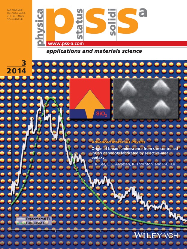
GaN/InGaN nanostructures have numerous potential electronic and opto-electronic applications, such as energy-selective contacts for hot carrier solar cells and light-emitting diodes. A joint experimental and computational approach has been developed to understand the properties of GaN/InGaN nanostructures grown by selective area epitaxy (see the article by P.-C. Ku and co-workers, pp. 531–535). GaN quantum dots were grown by metal-organic chemical vapor deposition on a GaN substrate, with a SiO2 mask patterned by electron-beam lithography used to control the initial quantum dot size and position. The morphology of the quantum dot in the early stages of deposition is non-uniform, resembling a volcano that gradually fills in and finally takes the shape of a hexagonal pyramid (inset, right). To understand the evolution of the morphology, a phase-field model was developed to simulate the growth process (inset, left), which included crystallographic orientation-dependent GaN growth and surface diffusion. Good agreement between simulation and experiment was obtained throughout the growth process. The growth of InGaN layers embedded in the quantum dots was also simulated, and the results were used to explain why the measured photoluminescence spectrum was considerably broader than expected.
Back Cover
Interfacial intermixing in SrRuO3/Pr0.7Ca0.3MnO3 epitaxial superlattices: A HAADF-STEM study (Phys. Status Solidi A 3∕2014)
- First Published: 18 March 2014
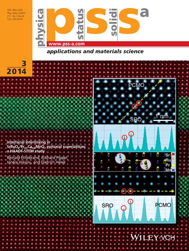
Perovskite superlattices show a large variety of useful physical properties, like (anti)ferromagnetism, (anti)ferroelectricity, superconductivity and multiferroicity. These properties may strongly depend on the interface morphology. In the article by Reinald Hillebrand et al. (see pp. 536–542), high angle annular dark field scanning transmission electron micrographs (HAADF-STEM) of SrRuO3/Pr0.7Ca0.3MnO3 (SRO/PCMO) superlattices are interpreted quantitatively. The superlattices were fabricated by pulsed-laser deposition (PLD). The growth was performed at a temperature of 650 °C and in an oxygen partial pressure of 0.14 mbar. The images were taken in the probe-corrected (cs = 0) FEI microscope TITAN 80-300 at 300 kV. The experimental studies have been substantially supported by image simulations. The specimen thickness is estimated by comparing experimental and simulated Z-contrast ratios. The quantitative image analyses proved that the intermixing at the interfaces is different for the growth of SRO on PCMO and that of PCMO on SRO. In addition, the thermal stability of SRO/PCMO superlattices is studied, based on a series of annealing experiments up to 1200 °C.
Issue Information
Contents
Recent and forthcoming publications in pss
Recent and forthcoming publications in pss
- Page: 529
- First Published: 18 March 2014
Advanced Materials Physics
Origin of broad luminescence from site-controlled InGaN nanodots fabricated by selective-area epitaxy
- Pages: 531-535
- First Published: 31 January 2014
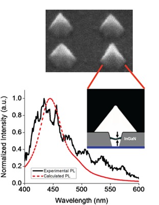
GaN nanodots with embedded InGaN layers are grown by selective area epitaxy. Photoluminescence measurements show significant energy state broadening compared to disk-shaped emitters of uniform thickness. Phase-field simulation of the growth process reveals an unexpected thickness variation in the InGaN layer. The photoluminescence spectrum calculated from the simulated InGaN layer profile agrees with the measured spectrum, demonstrating that the layer non-uniformity was the cause of the energy state broadening.
Original Papers
Interfacial intermixing in SrRuO3/Pr0.7Ca0.3MnO3 epitaxial superlattices: A HAADF-STEM study
- Pages: 536-542
- First Published: 04 December 2013
Temperature-dependent electrical characterization of exfoliated β-Ga2O3 micro flakes
- Pages: 543-549
- First Published: 19 February 2014
Frontispiece
Role of metal/silicon semiconductor contact engineering for enhanced output current in micro-sized microbial fuel cells (Phys. Status Solidi A 3∕2014)
- Page: 550
- First Published: 18 March 2014
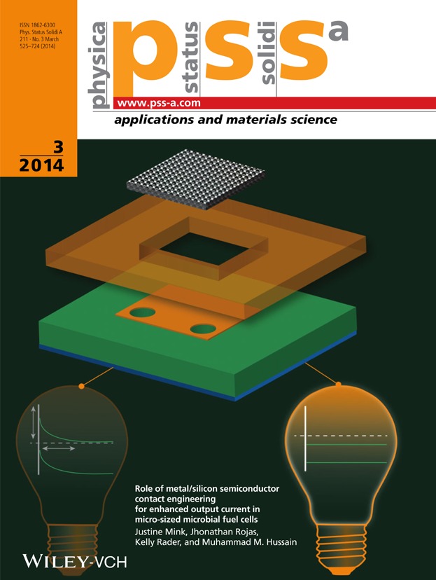
The metal-semiconductor contact plays an important role to define the performance of a device where current extraction is critical. In that regard, Mink et al. (pp. 551–554) examined a set of metals (Al, Ti, Co) fabricated as Ohmic and Schottky contact to study which can enable better performance in micro-sized microbial fuel cells fabricated on silicon. The study shows that, in general AlSix (Ohmic contacts) provide higher current density whereas CoSi2 Ohmic contacts provide higher power density.
Original Papers
Role of metal/silicon semiconductor contact engineering for enhanced output current in micro-sized microbial fuel cells
- Pages: 551-554
- First Published: 25 November 2013
The effect of samarium doping on structure and enhanced thermionic emission properties of lanthanum hexaboride fabricated by spark plasma sintering
- Pages: 555-564
- First Published: 11 November 2013
Evolution of parasitic phases with growth temperature in sputtered BiFeO3 thick films and their effect on magnetic properties
- Pages: 565-569
- First Published: 11 November 2013
Characteristics of ZnO Schottky photodiode and effects of high-energy proton irradiation
- Pages: 570-573
- First Published: 11 November 2013
Electro-elastic properties of YCa4O(BO3)3 piezoelectric crystals
- Pages: 574-579
- First Published: 12 November 2013
Fabrication and characterization of Al/Cu2ZnSnS4/n-Si/Al heterojunction photodiodes
- Pages: 580-586
- First Published: 12 November 2013
Effect of boron addition on interface microstructure and thermal conductivity of Cu/diamond composites produced by high temperature–high pressure method
- Pages: 587-594
- First Published: 12 November 2013
Precursor-controlled synthesis of different ZnO nanostructures by the hydrothermal method
- Pages: 595-600
- First Published: 13 November 2013
Improvement effect of electrical properties in post-annealed wafer-bonded Ge(001)-OI substrate
- Pages: 601-605
- First Published: 11 February 2014
Effects of annealing and MgO thickness on perpendicular magnetic anisotropy in Pt/Co2FeAl0.5Si0.5/MgO/Pt multilayers
- Pages: 606-610
- First Published: 20 November 2013
Effect of the orthorhombic/rhombohedral volume ratio on the piezoelectric properties of BaCaxTiO3–0.04LiF ceramics
- Pages: 611-617
- First Published: 20 November 2013
Thermoelectric properties of Cu2Ga4Te7 based compounds with Zn substitution for Cu and Ga
- Pages: 618-624
- First Published: 13 February 2014
Investigation of ZnO nanostructures grown on Si and GaAs substrates by low-temperature CBD method
- Pages: 625-629
- First Published: 20 November 2013
Effects of Y2O3 on mechanical, dielectric, and microwave-absorbing properties of short carbon-fiber/Al2O3 composites
- Pages: 630-635
- First Published: 29 November 2013
Magnetron sputtering of epitaxial ZrB2 thin films on 4H-SiC(0001) and Si(111)
- Pages: 636-640
- First Published: 02 December 2013
Magnetostriction-strain-induced enhancement and modulation of photovoltaic performance in Si-p–n/TbxDy1−xFe2 composite
- Pages: 641-644
- First Published: 02 December 2013
Effect of indium doping on the properties of GeSb phase-change alloy
- Pages: 645-650
- First Published: 04 December 2013
White light emission from a blue polymer light emitting diode combined with YAG:Ce3+ nanoparticles
- Pages: 651-655
- First Published: 05 December 2013
Deep-ultraviolet AlGaN light-emitting diodes with variable quantum well and barrier widths
- Pages: 656-660
- First Published: 05 December 2013
Influence of iron contaminations on local and bulk magnetic properties of nonfunctionalized and functionalized multi-wall carbon nanotubes
- Pages: 661-669
- First Published: 05 December 2013
Correlation between nanostructural, optical, and photoelectrical properties of P3HT:SiNW nanocomposites for solar-cell application
- Pages: 670-676
- First Published: 05 December 2013
Functionalization of boron nitride nanoparticles and their utilization in epoxy composites with enhanced thermal conductivity
- Pages: 677-684
- First Published: 05 December 2013
Optimizing the electrical power output of a thermogenerator with the Gerstenmaier/Wachutka approach
- Pages: 685-695
- First Published: 21 December 2013
High saturation ferromagnetic behavior of Fe:BN nanoceramic
- Pages: 696-699
- First Published: 12 December 2013
Theoretical investigation of sensitivity enhancement in dielectric multilayer surface plasmon sensor
- Pages: 700-704
- First Published: 13 December 2013
Rectifying behavior and photoinduced characteristic in La-doped BaSnO3/p-Si heterojunctions
- Pages: 705-708
- First Published: 13 December 2013
Effect of growth temperature on structural, electrical, and optical properties of Gd-doped zinc oxide films
- Pages: 709-713
- First Published: 18 December 2013
Structural, optical and electrical properties of Sb doped and undoped AgIn1 − xGaxSe2 and Ag(InGa)5Se8 thin films
- Pages: 714-722
- First Published: 19 December 2013
Information for authors
Sign up for email alerts
Tools
![]()
In 2022, the youngest family member physica status solidi (RRL) – Rapid Research Letters is turning 15 years. To celebrate this milestone, we present a new virtual collection with invited articles.
![]()
As we celebrate the 60th anniversary year of the physica status solidi family, click here to access our continuously updated collection of invited articles written by authors and partners of the pss journals.