

Journal list menu

 Issue
Issuephysica status solidi c: Volume 12, Issue 8
Special Issue:17th International Conference on Extended Defects in Semiconductors (EDS 2014), see 1 further paper in Phys. Status Solidi A 212, No. 8 (2015)
1061-1191August 2015
Export Citations
Download PDFs
Cover Picture
Cover Picture: Phys. Status Solidi C 8/2015
- First Published: 20 August 2015
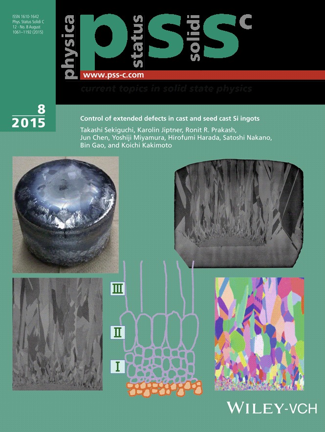
Multicrystalline silicon (mc-Si) grown by cast method has been most widely used for solar cell application. The improvement of mc-Si quality is the crucial issue for photovoltaics. There exist two directions for this purpose. One is the seed cast technique which can grow mono Si ingot free from GBs. The other is the controlled mc-Si growth, which is called high performance mc-Si. However, it is still not clear how the grain structure in mc-Si evolves and to which extent GBs can be controlled. In this study of Takashi Sekiguchi and coworkers (pp. 1094–1098), the authors have grown mc-Si from microcrystalline template. The grain evolution (low left) and electron backscattered diffraction (EBSD) pattern (low right) are analyzed and a three-step mechanism of grain growth was proposed.
Back Cover
Back Cover: Phys. Status Solidi C 8/2015
- First Published: 20 August 2015
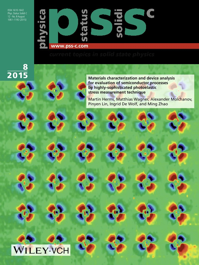
The layout of electronic systems of the next generation will be mainly three-dimensional. For vertical interconnections so-called TSVs (through silicon vias) are used. These are vertical holes filled with metal, e.g. copper. Resulting stress can affect the functionality of electronic devices and, a keep-out zone has to be defined. The integrity of TSV structures has to be tested by non-destructive analytical tools (see the paper of Martin Herms and coworkers on pp. 1085–1089). The figure shows a map of optical birefringence of a group of 6 × 6 single TSVs (ca. 500 μm × 500 μm) recorded with a photo-elastic microscope SIREX (Scanning Infrared Explorer). SIREX is a reflection-based plane polarimeter specially developed for the high-resolution stress state visualization in silicon-based electronic and mechanic devices. The diameter of a single TSV shown in the figure is 5 μm. Optical birefringence does occur if the silicon crystal matrix around the single TSV is optically anisotropic. The anisotropy revealed is caused by a radial stress field which is typical for point-like stress sources. The visualized “butterflies” represent the in-plane shear stress which can be converted into stress units in the order of a few kPa. The color sequence indicates the stress direction. Here, the TSVs generate a radial tensile stress component in the silicon matrix. Generally, magnitude, direction and lateral distribution of stress are determined by size and shape of a TSV but also by the presence of defects like voids.
Issue Information
Contents
Contents: Phys. Status Solidi C 8/2015
- Pages: 1061-1064
- First Published: 20 August 2015
Preface
Extended Defects in Semiconductors
- Pages: 1065-1066
- First Published: 20 August 2015
Contributed Articles
Dislocations in semiconductors
On the dislocation core structures associated to point defect cluster formation in diamond and silicon
- Pages: 1067-1070
- First Published: 15 July 2015
About dislocation and oxygen related luminescence of Si around 0.8 eV
- Pages: 1077-1080
- First Published: 11 May 2015
EBIC and LBIC investigations of dislocation trails in Si
- Pages: 1081-1084
- First Published: 05 June 2015
Materials characterization and device analysis for evaluation of semiconductor processes by highly-sophisticated photoelastic stress measurement technique
- Pages: 1085-1089
- First Published: 11 May 2015
The photoresponse of crystalline silicon strained via ultrasonic cavitation processing
- Pages: 1090-1093
- First Published: 28 July 2015
Invited Article
Extended defects in semiconductors for energy conversion
Control of extended defects in cast and seed cast Si ingots for photovoltaic application
- Pages: 1094-1098
- First Published: 05 June 2015
Contributed Articles
Extended defects in semiconductors for energy conversion
Control of extended defects in cast multicrystalline silicon using polycrystalline template
- Pages: 1099-1102
- First Published: 24 April 2015
Nanoscopic studies of 2D-extended defects in silicon that cause shunting of Si-solar cells
- Pages: 1103-1107
- First Published: 22 July 2015
Oxygen-related defects: minority carrier lifetime killers in n-type Czochralski silicon wafers for solar cell application
- Pages: 1108-1110
- First Published: 05 June 2015
Grain boundary recombination in semiconductors: the grain boundary interaction case
- Pages: 1111-1114
- First Published: 22 July 2015
Extended defects in MBE-grown CdTe-based solar cells
- Pages: 1115-1118
- First Published: 05 June 2015
Surface damage and mechanical strength of silicon wafers
- Pages: 1119-1122
- First Published: 28 July 2015
Extended defects in wide bandgap materials
Electronic structure of threading dislocations in wurtzite GaN
- Pages: 1123-1128
- First Published: 13 May 2015
Cathodoluminescence study of optical properties along the growth direction of ZnO films on GaN substrate
- Pages: 1129-1131
- First Published: 22 July 2015
Peculiarities of defect generation under injection current in LEDs based on group-III nitride3N nanostructures
- Pages: 1136-1139
- First Published: 11 May 2015
Study of the structural and magnetic properties of Fe-doped ZnO
- Pages: 1140-1143
- First Published: 22 July 2015
Structural, electrical and luminescent properties of ZnO:Li films fabricated by screen-printing method on sapphire substrate
- Pages: 1144-1147
- First Published: 05 June 2015
Epitaxial layers and heterostructures
Structural studies of Al thin layer on misoriented GaAs(100) substrate by transmission electron microscopy
- Pages: 1148-1151
- First Published: 05 June 2015
Impact of bismuth incorporation into (Ga,Mn)As thin films on their structural and magnetic properties
- Pages: 1152-1155
- First Published: 05 June 2015
Implantation, doping and irradiation
Hydrogen induced growth and coalescence of helium-based defects
- Pages: 1156-1159
- First Published: 15 July 2015
Impact of dopants and silicon structure dimensions on {113}-defect formation during 2 MeV electron irradiation in an UHVEM
- Pages: 1160-1165
- First Published: 13 May 2015
Atomic redistribution of implanted Fe and associated defects around moving SiO2/Si interfaces
- Pages: 1166-1169
- First Published: 05 June 2015
Properties of near-surface layer of 64Zn+ ion hot-implanted Si
- Pages: 1170-1174
- First Published: 22 July 2015
Nano-scale pattern formation on the surface of HgCdTe produced by ion bombardment
- Pages: 1175-1178
- First Published: 22 July 2015
Nanostructures and disordered materials
Turbostratic pyrocarbon structure study by means of exit wave reconstruction from high-resolution transmission electron microscopy
- Pages: 1179-1182
- First Published: 05 June 2015
Thermal activation and temperature dependent PL and CL of Tb doped amorphous AlN and SiN thin films
- Pages: 1183-1186
- First Published: 22 July 2015
Two-energy-scale model for description of the thermal quenching of photoluminescence in disordered Ga(As,Bi)
- Pages: 1187-1190
- First Published: 05 June 2015
leer
Retraction: Poly(3-hexylthiophene) films by electrospray deposition for crystalline silicon/organic hybrid junction solar cells
- Page: 1191
- First Published: 07 July 2015