Back Cover: Phys. Status Solidi C 8/2015
Graphical Abstract
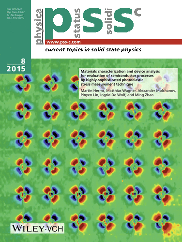
The layout of electronic systems of the next generation will be mainly three-dimensional. For vertical interconnections so-called TSVs (through silicon vias) are used. These are vertical holes filled with metal, e.g. copper. Resulting stress can affect the functionality of electronic devices and, a keep-out zone has to be defined. The integrity of TSV structures has to be tested by non-destructive analytical tools (see the paper of Martin Herms and coworkers on pp. 1085–1089). The figure shows a map of optical birefringence of a group of 6 × 6 single TSVs (ca. 500 μm × 500 μm) recorded with a photo-elastic microscope SIREX (Scanning Infrared Explorer). SIREX is a reflection-based plane polarimeter specially developed for the high-resolution stress state visualization in silicon-based electronic and mechanic devices. The diameter of a single TSV shown in the figure is 5 μm. Optical birefringence does occur if the silicon crystal matrix around the single TSV is optically anisotropic. The anisotropy revealed is caused by a radial stress field which is typical for point-like stress sources. The visualized “butterflies” represent the in-plane shear stress which can be converted into stress units in the order of a few kPa. The color sequence indicates the stress direction. Here, the TSVs generate a radial tensile stress component in the silicon matrix. Generally, magnitude, direction and lateral distribution of stress are determined by size and shape of a TSV but also by the presence of defects like voids.


