

Journal list menu

 Issue
Issuephysica status solidi c: Volume 8, Issue 3
Special Issue:E‐MRS 2010 Spring Meeting – Symposium I: Advanced Silicon Materials Research for Electronic and Photovoltaic Applications II • E‐MRS 2010 Spring Meeting – Symposium J: Silicon‐based Nanophotonics
641-1096March 2011
Export Citations
Download PDFs
Cover Picture
Cover Picture: Phys. Status Solidi C 3/2011
- First Published: 11 March 2011
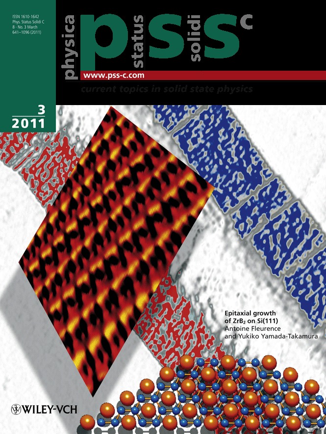
In their article on pp. 779ff., A. Fleurence and Y. Yamada-Takamura evidence by means of scanning tunneling microscopy that the formation of homogeneous ZrB2(0001) thin films is hindered by the nucleation of misoriented ZrB2 crystallites. The cover picture shows one of these parasitic structures. Its existence is unambiguously related to the formation of (1 00) facets, the stability of which is speculated to be originating in the (2 × 6) surface reconstruction we report here for the first time. Based on these experimental observations, they propose solutions to prevent the formation of these parasitic crystallites which will lead to better integration of III-nitrides with silicon.
Back Cover
Back Cover: Phys. Status Solidi C 3/2011
- First Published: 11 March 2011
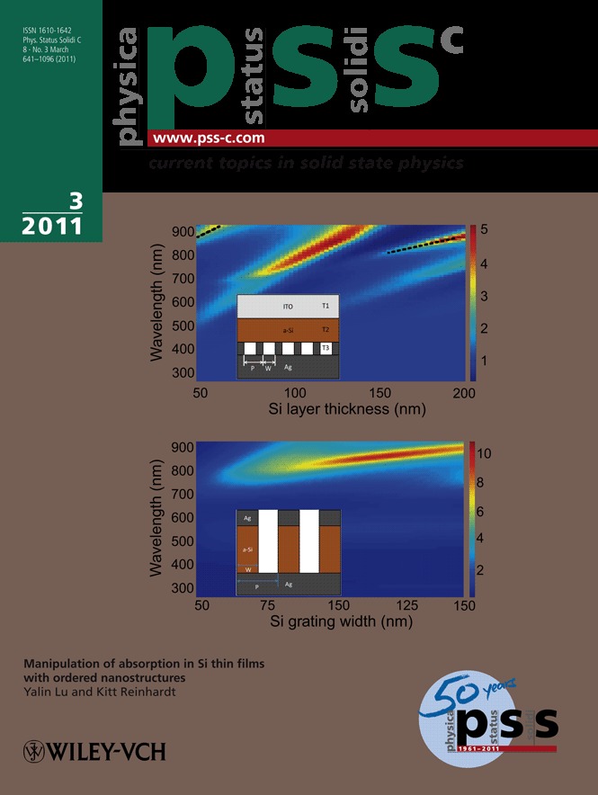
In their article on pp. 839ff., Yalin Lu and Kitt Reinhardt investigate the use of two nanostructure designs in solar cells, with the goal to enhance both light absorption and current density. The pictures show absorption in the solar spectrum using an embedded nanograting (top) and a through-grating nanostructures (bottom), over the Si layer thickness and the Si grating width, respectively. Both cases are under TM incidence.
Prof. Yalin Lu's working fields include photonics, nanomaterials, energy materials, etc.
Inside Front Cover
Inside Front Cover: Phys. Status Solidi C 3/2011
- First Published: 11 March 2011
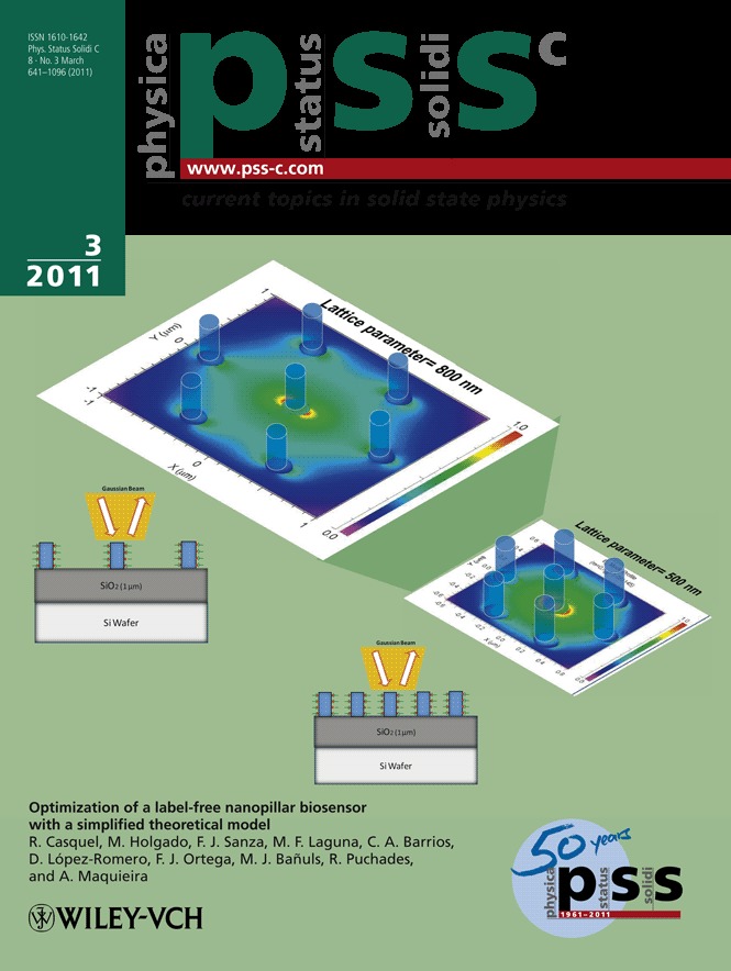
The research activities of the Micro–nano Biophotonics Group at the Centro Láser UPM are focused on the design, fabrication and characterization of sub micro patterned biophotonic sensing cells (BICELLs), characterized using vertical coupling techniques. In their work on pp. 1087, R. Casquel and coworkers develop a simplified theoretical method which allows the optimization of a SU-8 pillar based BICELL, previously fabricated and demonstrated as biosensor by using antiBSA/BSA immunoreaction. 3D FDTD calculations, experimental results and proposed model calculations are compared. The suitability of the method allows to obtain values for expected biodetection limits for a variety of geometrical configurations.
Issue Information
Contents
Preface
Preface – Symposium I: Phys. Status Solidi C 3/2011
- Pages: 653-654
- First Published: 11 March 2011
Obituary
Ulrich Gösele – 35 years of research: From defects and diffusion to nanomaterials
- Pages: 655-658
- First Published: 17 December 2010
EMRS-I – Invited Articles
Point defects, impurities, defect complexes and compensation effects
Numerical analysis of light elements transport in a unidirectional solidification furnace
- Pages: 659-661
- First Published: 11 March 2011
Selection of silicon wafer for power devices and the influence of crystal defects including impurities
- Pages: 662-665
- First Published: 20 January 2011
EMRS-I – Contributed Articles
Point defects, impurities, defect complexes and compensation effects
Study of oxygen clustering in Czochralski silicon at 450 °C–800 °C: correlation with thermal donors formation
- Pages: 666-669
- First Published: 13 January 2011
Dopant diffusivity and solubility in nickel silicides
- Pages: 670-673
- First Published: 13 January 2011
Electron irradiation induced defects in germanium-doped Czochralski silicon substrates and diodes
- Pages: 674-677
- First Published: 23 November 2010
Ga co-doping in Cz-grown silicon ingots to overcome limitations of B and P compensated silicon feedstock for PV applications
- Pages: 678-681
- First Published: 20 January 2011
Quantumchemical simulation of diffusion in alloys: diffusion of interstitial oxygen atoms in Si1-xGex
- Pages: 682-685
- First Published: 17 December 2010
Effects of uniaxial stress on local vibration of a platinum-hydrogen complex in silicon
- Pages: 686-689
- First Published: 15 November 2010
First-principles calculation on screw defects at Si(110)/(100) interface
- Pages: 690-693
- First Published: 13 January 2011
Interaction of point defects with impurities in the Si-SiO2 system and its influence on the interface properties
- Pages: 694-696
- First Published: 22 December 2010
Dopant profiles in silicon created by MeV hydrogen implantation: Influence of annealing parameters
- Pages: 697-700
- First Published: 23 November 2010
IR studies of oxygen-related and carbon-related defects in Sn-doped silicon
- Pages: 701-704
- First Published: 15 November 2010
Hydrogen-related defects in boron doped p-type silicon
- Pages: 705-708
- First Published: 22 December 2010
Local vibrational modes of the oxygen trimer in Si
- Pages: 709-712
- First Published: 13 January 2011
Relationship between net doping density and resistivity of compensated mc-Si ingots
- Pages: 713-716
- First Published: 23 November 2010
First-principles study on initial stage of oxidation on Si(110) surface
- Pages: 717-720
- First Published: 13 January 2011
Lifetime and DLTS studies of interstitial Fe in p-type Si
- Pages: 721-724
- First Published: 22 December 2010
Electrically active centers introduced in p-type Si by rapid thermal processing
- Pages: 725-728
- First Published: 22 December 2010
Hall mobility drops in disordered boron-doped Czochralski silicon compensated by thermal donors activation
- Pages: 729-732
- First Published: 17 December 2010
EMRS-I – Invited Article
Gettering passivation and defect engineering
Research on efficiency limiting defects and defect engineering in silicon solar cells - results of the German research cluster SolarFocus
- Pages: 733-738
- First Published: 22 December 2010
EMRS-I – Contributed Articles
Gettering passivation and defect engineering
Structure of the near-surface layer of Cz Si wafers subjected to low-temperature low-energy ion-beam treatment
- Pages: 739-742
- First Published: 20 January 2011
Phosphorous gettering in acidic textured multicrystalline solar cells
- Pages: 743-746
- First Published: 17 December 2010
A comparative study on different textured surfaces passivated with amorphous silicon
- Pages: 747-750
- First Published: 17 December 2010
Gettering of iron in CZ-silicon by polysilicon layer
- Pages: 751-754
- First Published: 23 November 2010
Improvement of solar cells performances by surface passivation using porous silicon chemically treated with LiBr solution
- Pages: 755-758
- First Published: 13 January 2011
Enhanced iron gettering by short, optimized low-temperature annealing after phosphorus emitter diffusion for industrial silicon solar cell processing
- Pages: 759-762
- First Published: 20 January 2011
Comprehensive investigation of silicon surface passivation by a -Si:H and a -SiNx:H films
- Pages: 763-766
- First Published: 22 December 2010
Influence of precipitates on the kinetics of iron gettering from the Si wafers by the Al layers
- Pages: 767-770
- First Published: 23 November 2010
Characterization techniques and advanced methods of defect diagnostics
Growth rate model and doping metrology by atom probe tomography in silicon nanowire
- Pages: 771-774
- First Published: 17 December 2010
Spatially resolved lifetime measurements of silicon heterojunctions from the modulated photoluminescence technique
- Pages: 775-778
- First Published: 13 January 2011
Scanning tunneling microscopy investigations of the epitaxial growth of ZrB2 on Si(111)
- Pages: 779-783
- First Published: 22 December 2010
Investigation of current-voltage characteristics of p-type silicon during electrochemical anodization and application to doping profiling
- Pages: 784-787
- First Published: 20 January 2011
Decoration and preferential etching of crystal defects in silicon materials: influence of metal decoration on the defect etching process
- Pages: 788-791
- First Published: 20 January 2011
Quantitative analysis of impurities in solar-grade Si by photoluminescence spectroscopy around 20 K
- Pages: 792-795
- First Published: 23 November 2010
Chemical characterization of SiC and Si3N4 precipitates in multicrystalline silicon by NIR microscopy and ToF-SIMS
- Pages: 796-799
- First Published: 22 December 2010
Solar grade silicon, silicon thin films, amorphous silicon, silicon nanocrystals, nanowires and naonodots
Role of carbon content in tuning the physical quantities of a-Si1-xCx:H alloys deposited by PECVD
- Pages: 800-803
- First Published: 22 December 2010
Stoichiometry of silicon-rich dielectrics for silicon nanocluster formation
- Pages: 804-807
- First Published: 20 January 2011
Diffusion length determination in solar grade silicon by room temperature photoluminescence measurements
- Pages: 808-811
- First Published: 17 December 2010
Confined growth of silicon nanowires as a possible process for third generation solar cells
- Pages: 812-815
- First Published: 22 December 2010
Electrical characterisation of Si-SiO2 structures
- Pages: 816-818
- First Published: 15 November 2010
Simulations of silicon nanocrystals embedded in oxide for nanoelectronic applications
- Pages: 819-822
- First Published: 22 December 2010
Influence of rf power on the properties of nanostructured silicon-carbon films deposited by PECVD
- Pages: 823-826
- First Published: 13 January 2011
Electrical properties of polysilicon nanowires for device applications
- Pages: 827-830
- First Published: 17 December 2010
Si and SiC nanocrystals in an amorphous SiC matrix: Formation and electrical properties
- Pages: 831-834
- First Published: 23 November 2010
Carrier mobilities in multicrystalline silicon wafers made from UMG-Si
- Pages: 835-838
- First Published: 23 November 2010
Manipulation of absorption in Si thin films with ordered nanostructures
- Pages: 839-842
- First Published: 17 December 2010
Adding a thin metallic plasmonic layer to silicon thin film solar cells
- Pages: 843-845
- First Published: 17 December 2010
High-rate deposition of nano-crystalline silicon thin films on plastics
- Pages: 846-849
- First Published: 13 January 2011
Variation in the structure and optical properties of polymorphous silicon thin films using dichlorosilane as silicon precursor
- Pages: 850-853
- First Published: 17 December 2010
Compensated silicon crystals by metallurgy route
- Pages: 854-858
- First Published: 15 November 2010
Microstructural tuning of polycrystalline silicon films from hydrogen diluted amorphous silicon films by AIC
- Pages: 859-862
- First Published: 20 January 2011
Analyses of the As doping of SiO2/Si/SiO2 nanostructures
- Pages: 863-866
- First Published: 15 November 2010
EMRS-I – Invited Articles
Devices, alternative growth and doping processes, modeling
Material effects in manufacturing of silicon based solar cells and modules
- Pages: 871-874
- First Published: 22 December 2010
EMRS-I – Contributed Articles
Devices, alternative growth and doping processes, modeling
Temperature effect on an N-channel commercial VDMOSFET transistor
- Pages: 875-878
- First Published: 25 January 2011
Effect of wet-chemical substrate pretreatment on electronic interface properties and recombination losses of a -Si:H/c -Si and a -SiNx:H/c -Si hetero-interfaces
- Pages: 879-882
- First Published: 17 December 2010
Reduction of absorption loss in multicrystalline silicon via combination of mechanical grooving and porous silicon
- Pages: 883-886
- First Published: 23 November 2010
Optoelectronic enhancement of monocrystalline silicon solar cells by porous silicon-assisted mechanical grooving
- Pages: 887-890
- First Published: 17 December 2010
Atomic-layer-deposited Ir thin film as a novel diffusion barrier layer in Cu interconnection
- Pages: 891-894
- First Published: 23 November 2010
Stability against hydrogen plasma exposure of Al-doped zinc oxide thin film for a-Si thin film solar cell
- Pages: 895-898
- First Published: 03 January 2011
Analytical modelling and experimental verification of the three-dimensional current distribution on the top surface of silicon solar cells operating under concentrated sunlight
- Pages: 899-902
- First Published: 17 December 2010
An analytical drain current model for undoped GSDG MOSFETs including interfacial hot-carrier effects
- Pages: 907-910
- First Published: 23 November 2010
Anomalous temperature behaviour of band to band electroluminescence in silicon solar cells
- Pages: 911-914
- First Published: 23 November 2010
Pseudomorphic and relaxed SiGe/Si(001) layer synthesis by gas immersion laser doping (GILD)
- Pages: 915-918
- First Published: 20 January 2011
Integrated demultiplexer and photodetector for short range transmission in the visible range
- Pages: 919-923
- First Published: 23 November 2010
Chemical synthesis of silver nanoparticles for solar cell applications
- Pages: 924-927
- First Published: 22 December 2010
Heterojunction solar cells on multi- crystalline silicon: surface treatments
- Pages: 928-931
- First Published: 22 December 2010
Back contact formation for p-type based a-Si:H/c-Si heterojunction solar cells
- Pages: 932-935
- First Published: 22 December 2010
Implantation and irradiation defects
FEM for modelling 193 nm excimer laser treatment of SiO2/Si/Si(1-x)Gex heterostructures on SOI substrates
- Pages: 936-939
- First Published: 22 December 2010
Dopant activation and damage evolution in implanted silicon after excimer laser annealing
- Pages: 940-943
- First Published: 17 December 2010
Decoupling of a strained 3C-SiC(111) thin film on silicon by He+ and O+ ion implantation
- Pages: 944-947
- First Published: 20 January 2011
Interaction of hydrogen and deuterium with radiation defects introduced in silicon by high-energy helium irradiation
- Pages: 948-951
- First Published: 13 January 2011
Highly strained Si epilayers grown on SiGe/Si(100) virtual substrate by reduced pressure chemical vapour deposition
- Pages: 952-955
- First Published: 17 December 2010
Defects formed by pulsed laser annealing: electrical properties and depth profiles in n-type silicon measured by deep level transient spectroscopy
- Pages: 956-959
- First Published: 23 November 2010
The formation of near surface SiGe layers with combined high-dose ion implantation and flash-lamp annealing
- Pages: 960-963
- First Published: 23 November 2010
Preface
Preface – Symposium J: Phys. Status Solidi C 3/2011
- Pages: 967-968
- First Published: 11 March 2011
EMRS-J – Contributed Articles
Nonlinear optical properties of Si nanocrystals
Comparative study of the nonlinear optical properties of Si nanocrystals fabricated by e-beam evaporation, PECVD or LPCVD
- Pages: 969-973
- First Published: 01 February 2011
Radiative and non-radiative recombination in Si-based materials
On the role of non-bridging oxygen centers in the red luminescence emission from silicon nanocrystals
- Pages: 974-978
- First Published: 25 January 2011
Ultrafast photoluminescence dynamics of blue-emitting silicon nanostructures
- Pages: 979-984
- First Published: 25 January 2011
Theory of nonradiative transitions of hot carriers in Si/SiO2 nanocrystals
- Pages: 985-990
- First Published: 01 February 2011
Structures responsible for radiative and non-radiative recombination activity of dislocations in silicon
- Pages: 991-995
- First Published: 25 January 2011
Optical properties and size/shape dependence of α-Sn nanocrystals by tight binding
- Pages: 1002-1005
- First Published: 01 February 2011
Silicon nanowires and nanorods
Temperature and directional dependences of the infrared dielectric function of free standing silicon nanowire
- Pages: 1006-1011
- First Published: 25 January 2011
Scanning confocal Raman spectroscopy of silicon phase distribution in individual Si nanowires
- Pages: 1012-1016
- First Published: 01 February 2011
Polarization of photoluminescence excitation and emission spectra of silicon nanorods within single Si/SiO2 nanowires
- Pages: 1017-1020
- First Published: 01 February 2011
Er-doped nanostructures
Effects of the thickness on the properties of erbium-doped silicon-rich silicon oxide thin films
- Pages: 1027-1032
- First Published: 25 January 2011
Excitation of erbium ions in SiO2 with Si nanocrystals via virtual Auger process
- Pages: 1033-1037
- First Published: 01 February 2011
The spatial distribution of silicon NCs and erbium ion clusters by simultaneous high-resolution energy filtered and Z-contrast STEM and transmission electron tomography
- Pages: 1038-1043
- First Published: 25 January 2011
On the role of heterolayer relaxation in luminescence response of Si/SiGe:Er structures
- Pages: 1044-1048
- First Published: 25 January 2011
EMRS-J – Invited Article
Silicon–germanium nanostructures
Auger recombination in Si1-xGex/Si quantum wells under high-density photoexcitation
- Pages: 1049-1054
- First Published: 25 January 2011
EMRS-J – Contributed Articles
Silicon–germanium nanostructures
Narrow photoluminescence peak from Ge(Si) islands embedded between tensile-strained Si layers
- Pages: 1055-1059
- First Published: 01 February 2011
Photonic structures: Microcavities, photonic crystals and waveguides
Optically active substoichiometric Si3N4 μ-cavities
- Pages: 1060-1065
- First Published: 01 February 2011
Photonic stop bands of two-dimensional quasi-random structures based on macroporous silicon
- Pages: 1066-1070
- First Published: 01 February 2011
Garnet photonics toward developing laser diode integrated with optical isolator with Si guiding layer
- Pages: 1071-1074
- First Published: 01 February 2011
Tunable waveguides based on liquid crystal-infiltrated silicon photonic crystals
- Pages: 1075-1078
- First Published: 01 February 2011
Si nanostructures for light detection and sensing
Photo-sensing devices using a-Si based materials
- Pages: 1079-1082
- First Published: 25 January 2011
Light-triggered silicon-carbon pi'npin devices with self amplification
- Pages: 1083-1086
- First Published: 25 January 2011
Optimization of a label-free biosensor vertically characterized based on a periodic lattice of high aspect ratio SU-8 nano-pillars with a simplified 2D theoretical model
- Pages: 1087-1092
- First Published: 01 February 2011