Journal list menu

 Issue
Issuephysica status solidi (a): Volume 214, Issue 8
August 2017
Export Citations
Download PDFs
Cover Picture
Plasmon resonance coupling phenomena in self-assembled colloidal monolayers (Phys. Status Solidi A 8∕2017)
- First Published: 14 August 2017

Noble metal nanoparticles such as gold and silver support localized surface plasmon resonances upon excitation by visible light. When brought into close proximity or arranged in periodic arrays, these single particle resonances interfere leading to collective, coupled optical response. Tailoring the strength and frequency of the coupled resonance is an important prerequisite for the suitability of such materials for modern nanophotonic applications including sensing, high resolution microscopy and plasmonic lasing. Here, Fitzgerald and Karg (article no. 1600947) review recent works that demonstrate defined plasmon coupling phenomena in self-assembled colloidal monolayers. Design concepts and properties of plasmonic building blocks are presented followed by an introduction to single particle and coupled plasmon resonances. Then examples for near-field, plasmonic/diffractive as well as anisotropic coupling are introduced. Overall, this review highlights the benefits of wet-chemical synthesis for the fabrication of functional building blocks in combination with the flexibility of colloidal self-assembly offering access to high-troughput nanostructuring on application-relevant, macroscopic areas.
Inside Cover
Defect related radiative recombination in mono-like crystalline silicon wafers (Phys. Status Solidi A 8∕2017)
- First Published: 14 August 2017
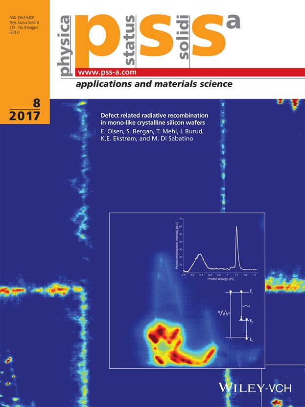
In order to improve wafer based silicon solar cell performance with even lower costs, new methods for manufacturing the material are constantly being developed. One approach is to use low cost block casting to make material with primarily monocrystalline character, called mono-like silicon. Unfortunately, crystal faults readily form and multiply in this structure. These cause the recombination of photogenerated charge carriers lowering the efficiency of solar cells. The socalled D-line emissions are four luminescence signals (D1–D4) emanating from photoexcited silicon. They are caused by radiative recombination via traps in the band gap and are reported to always occur together in dislocated areas. The behaviour of the D-line emissions as function of position in a block of mono-like silicon has been studied by Olsen et al. (article no. 1700124). The emissions behave differently suggesting they do not have the same origin. A new signal (0.70 eV) is found in areas where the mono-like character is lost due to formation of material with multicrystalline character. These areas are highly dislocated, however do not exhibit the D1–D4 emissions.
Issue Information
Inside Back Cover
Techniques to reduce thermal resistance in flip-chip GaN-based VCSELs (Phys. Status Solidi A 8∕2017)
- First Published: 14 August 2017
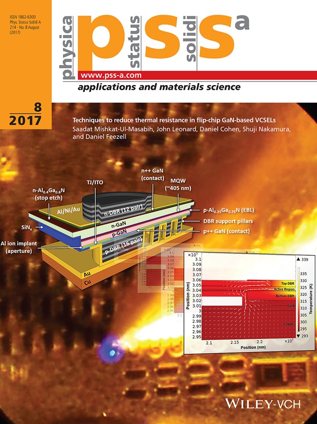
The effects of several design geometries on the thermal resistance for a flip-chip GaN-based VCSEL with dielectric distributed Bragg reflectors was studied by Mishkat-Ul- Masabih (article no. 1600819) using finite-element analysis. The current flip-chip design suffers from high thermal resistance, preventing devices to lase under CW operation. It was found that including a patterned DBR with recessed metal, reducing the lithography alignment tolerances, and increasing the aperture size; all contributed to the reduction of the thermal resistance of the design. In addition, epitaxially increasing the cladding layer thickness on either side of the active region also lowered the thermal resistance significantly. The thermal resistance values for previously reported CW device configurations were also calculated and compared to our flip-chip design. The internal temperature changes at the threshold were estimated for the devices, indicating why previous generations of our flip-chip devices could not achieve CW lasing. Combining these techniques, the effects of thermal roll-over can be mitigated; as the reduction of the device temperature is a key consideration for obtaining high output power CW GaN-based VCSELs.
Back Cover
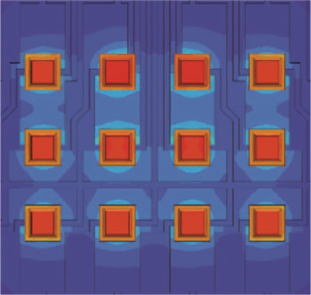
Facet dependence of leakage current and carrier concentration in m-plane GaN Schottky barrier diode fabricated with MOVPE (Phys. Status Solidi A 8∕2017)
- First Published: 14 August 2017
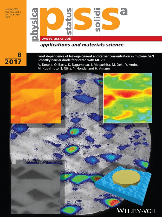
The background of this cover page shows a superimposed emission microscope image observed from backside of a GaN m-plane Schottky barrier diode with reverse biased condition. It can be observed that the epitaxial layer of m-plane GaN has pyramidal hillocks at the surface, and only facets inclined toward the [0001] direction (+c facet) have emission due to leakage current. Three images at the corner are differential interference contrast microscopy image (upper left), photoluminescence intensity mapping image (PL, upper right), and cathode luminescence image (CL, lower left), respectively, observing the same pyramidal hillocks to investigate the characteristics of each facet. The PL image indicates the intensity of near-band-edge emission (around 363 nm wavelength) of the facets. Details are discussed in the article by Tanaka et al. (no. 1600829). The +c facets have high emission intensity, indicating that there is a high impurity concentration in the +c facets. Furthermore, we consider this is the reason that +c facets have high leakage current. The CL image is a panchromatic image, and facets inclined toward [000-1] direction (−c facet) have lowest emission. Together with PL intensity mapping it can be considered that −c facets have less yellow emission and less impurity concentration.
Contents
Preface
Feature Article
Light-emitting diodes
Progress in high-luminance LED technology for solid-state lighting
- First Published: 22 March 2017
Increasing the luminance of white LEDs to the 200 Mnit level and beyond opens a completely new design space for a wide range of lighting applications, by allowing significant reductions in optics and luminaire size as well as cost. Moreover, new applications such as dynamic beam steering are enabled by the ability to create arrays of densely packed, individually addressable high-luminance emitters. Development of such high-luminance LEDs requires improvements in all LED technology elements. In this paper, the authors discuss recent advances in epitaxy, die, phosphor and package technology that are critical to achieving these benefits.
Original Papers
Light-emitting diodes
Improved light output power of GaN-based ultraviolet light-emitting diode using a mesh-type GaN/SiO2/Al omnidirectional reflector
- First Published: 27 March 2017
Reducing forward voltage and enhancing output performance of InGaN-based blue light-emitting diodes using metal dot-embedded transparent p-type finger
- First Published: 09 March 2017
Improvement of thermal stability of Ag-based reflector in GaN-based flip chip LEDs by electron-beam irradiation
- First Published: 17 February 2017
Depth dependent strain analysis in GaN-based light emitting diodes using surface-plasmon enhanced Raman spectroscopy
- First Published: 31 March 2017
V-shaped semipolar InGaN/GaN multi-quantum-well light-emitting diodes directly grown on c-plane patterned sapphire substrates
- First Published: 16 June 2017
Reduction of basal plane defects in (11–22) semipolar InGaN/GaN MQWs fabricated on patterned (113) Si substrates by introducing AlGaN barrier layers
- First Published: 22 March 2017
A resonant-cavity blue–violet light-emitting diode with conductive nanoporous distributed Bragg reflector
- First Published: 24 February 2017
Feature Article
Electronic devices
Low cost high voltage GaN polarization superjunction field effect transistors
- First Published: 18 April 2017
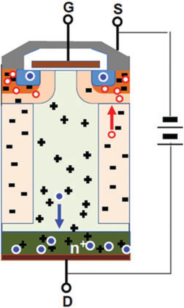
An overview of novel high-voltage polarization superjunction (PSJ) technology platform in GaN materials system is presented here. With extremely competitive performance trade-offs, PSJ devices are ideally suited for extreme operating conditions and can be used in space, aerospace, transportation, oil-drilling, industrial as well as consumer applications. A sustainable route towards manufacturing of PSJ-FETs, utilizing the existing and mature infrastructure for GaN LED production, is also discussed. With sapphire as the chosen substrate, PSJ is ideally suited for developing monolithic power integrated circuits which will be essential for practically realising high frequency power switching solutions using GaN.
Original Papers
Electronic devices
High-performance normally off AlGaN/GaN-on-Si HEMTs with partially recessed SiNx MIS structure
- First Published: 15 May 2017
Improved planar device isolation in AlGaN/GaN HEMTs on Si by ultra-heavy 131Xe+ implantation
- First Published: 21 July 2017
High power, high PAE Q-band sub-10 nm barrier thickness AlN/GaN HEMTs
- First Published: 15 May 2017
Switching performance of quasi-vertical GaN-based p-i-n diodes on Si
- First Published: 15 May 2017
Lossless turn-off switching projection of lateral and vertical GaN power field-effect transistors
- First Published: 18 July 2017
The influence of Al composition in AlGaN back barrier layer on leakage current and dynamic RON characteristics of AlGaN/GaN HEMTs
- First Published: 06 June 2017
Facet dependence of leakage current and carrier concentration in m-plane GaN Schottky barrier diode fabricated with MOVPE
- First Published: 04 July 2017
An AlGaN/GaN field effect diode with a high turn-on voltage controllability
- First Published: 20 April 2017
Dual barrier InAlN/AlGaN/GaN-on-silicon high-electron-mobility transistors with Pt- and Ni-based gate stacks
- First Published: 20 July 2017
Normally-off AlGaN/GaN MOS-HEMT using ultra-thin Al0.45Ga0.55N barrier layer
- First Published: 15 May 2017
Effect of dislocations on the growth of p-type GaN and on the characteristics of p–n diodes
- First Published: 24 February 2017
Analysis of carrier trapping and emission in AlGaN/GaN HEMT with bias-controllable field plate
- First Published: 16 June 2017
Other optical devices
Techniques to reduce thermal resistance in flip-chip GaN-based VCSELs
- First Published: 19 June 2017
GaN/Al0.1Ga0.9N-based visible-blind double heterojunction phototransistor with a collector-up structure
- First Published: 26 May 2017
Theoretical investigation of nitride nanowire-based quantum-shell lasers
- First Published: 12 June 2017
Preface
Photonic materials and techniques for SERS and solar cell light trapping
- First Published: 14 August 2017
Review Article
Photonic materials and techniques
Plasmon resonance coupling phenomena in self-assembled colloidal monolayers
- First Published: 30 June 2017
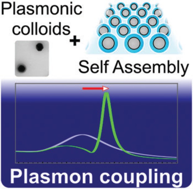
Optical nanostructures are a critical next-generation technology in which plasmonic surfaces play a keystone role. Here, recent advances in colloidal self-assembly approaches for the fabrication of functional monolayers showing plasmonic coupling phenomena are reviewed. The manner in which optical properties can be precisely engineered through the clever combination of wet-chemically synthesized building blocks with tailored optical response and template-free, as well as templated assembly strategies yielding isotropic and anisotropic superstructures, are highlighted.
Original Papers
Photonic materials and techniques
Strong coupling between localized surface plasmon and Bragg mode on aluminum nanocylinders grating deposited on aluminum film
- First Published: 21 June 2017
Aluminum induced texturing of sandy and prism glasses: Combination of micro/nano texture with macro texture
- First Published: 11 July 2017
Evaluation of light trapping structures for liquid-phase crystallized silicon on glass (LPCSG)
- First Published: 16 June 2017
Influence of ZnSnOx barrier layer on the texturing of ZnO:Al layers for light management in flexible thin-film silicon solar cells
- First Published: 28 June 2017
CaTiO3:Er3+,Ni2+ broadband-sensitive upconverter: An effective way to harvest unused NIR solar irradiation for crystalline silicon solar cells
- First Published: 09 June 2017
Microwave welding of silver nanowires for highly transparent conductive electrodes
- First Published: 28 July 2017
Phospholipid detection by surface-enhanced Raman scattering using silvered porous silicon substrates
- First Published: 11 July 2017
Flexible thin film solar cells on cellulose substrates with improved light management
- First Published: 27 July 2017
Regular contributions
Structural, electrical, and acoustical properties of graphene oxide films for acoustoelectronic applications
- First Published: 21 April 2017
Extraction of net acceptor type trap density in semi-insulating GaN layers grown on Si substrate by DC I–V measurement
- First Published: 21 April 2017
High electrical conductivity of composite ceramics consisting of insulating oxide and ordered perovskite conducting oxide
- First Published: 08 May 2017
Nanocrystalline and monophasic thin films of metal chalcogenide (FeS, ZnS) and oxide (ZnO) by chemical bath deposition (CBD)
- First Published: 18 April 2017
On the recombination behavior of p+-type polysilicon on oxide junctions deposited by different methods on textured and planar surfaces
- First Published: 08 May 2017
Thermal annealing effect on β-Ga2O3 thin film solar blind photodetector heteroepitaxially grown on sapphire substrate
- First Published: 09 May 2017
Highly improved charge injection in pentacene-based organic transistors by chemically doping with copper iodide interlayer
- First Published: 18 April 2017
In situ generated CdS nanostructure induced enhanced photoluminescence from Dy3+ ions doped dielectric nanocomposites
- First Published: 08 May 2017
Effect of Au nanoparticles on PCPDTBT:PC71BM device performance with fair comparisons
- First Published: 04 May 2017
Defect related radiative recombination in mono-like crystalline silicon wafers
- First Published: 27 April 2017
Information for authors
Sign up for email alerts
Tools
![]()
In 2022, the youngest family member physica status solidi (RRL) – Rapid Research Letters is turning 15 years. To celebrate this milestone, we present a new virtual collection with invited articles.
![]()
As we celebrate the 60th anniversary year of the physica status solidi family, click here to access our continuously updated collection of invited articles written by authors and partners of the pss journals.