Facet dependence of leakage current and carrier concentration in m-plane GaN Schottky barrier diode fabricated with MOVPE
Corresponding Author
Atsushi Tanaka
Institute of Materials and Systems for Sustainability, Nagoya University, Furo-cho, Chikusa-ku, 464-8603 Nagoya, Japan
Corresponding author: e-mail [email protected], Phone: +8152-789-5275, Fax: +8152-789-3156
Search for more papers by this authorOusmane1 Barry
Department of Electrical Engineering and Computer Science, Nagoya University, Furo-cho, Chikusa-ku, 464-8603 Nagoya, Japan
Search for more papers by this authorKentaro Nagamatsu
Institute of Materials and Systems for Sustainability, Nagoya University, Furo-cho, Chikusa-ku, 464-8603 Nagoya, Japan
Search for more papers by this authorJunya Matsushita
Department of Electrical Engineering and Computer Science, Nagoya University, Furo-cho, Chikusa-ku, 464-8603 Nagoya, Japan
Search for more papers by this authorManato Deki
Institute of Materials and Systems for Sustainability, Nagoya University, Furo-cho, Chikusa-ku, 464-8603 Nagoya, Japan
Search for more papers by this authorYuto Ando
Department of Electrical Engineering and Computer Science, Nagoya University, Furo-cho, Chikusa-ku, 464-8603 Nagoya, Japan
Search for more papers by this authorMaki Kushimoto
Department of Electrical Engineering and Computer Science, Nagoya University, Furo-cho, Chikusa-ku, 464-8603 Nagoya, Japan
Search for more papers by this authorShugo Nitta
Institute of Materials and Systems for Sustainability, Nagoya University, Furo-cho, Chikusa-ku, 464-8603 Nagoya, Japan
Search for more papers by this authorYoshio Honda
Institute of Materials and Systems for Sustainability, Nagoya University, Furo-cho, Chikusa-ku, 464-8603 Nagoya, Japan
Search for more papers by this authorHiroshi Amano
Institute of Materials and Systems for Sustainability, Nagoya University, Furo-cho, Chikusa-ku, 464-8603 Nagoya, Japan
Akasaki Research Center, Nagoya University, Furo-cho, Chikusa-ku, 464-8603 Nagoya, Japan
Venture Business Laboratory, Nagoya University, Furo-cho, Chikusa-ku, 464-8603 Nagoya, Japan
Search for more papers by this authorCorresponding Author
Atsushi Tanaka
Institute of Materials and Systems for Sustainability, Nagoya University, Furo-cho, Chikusa-ku, 464-8603 Nagoya, Japan
Corresponding author: e-mail [email protected], Phone: +8152-789-5275, Fax: +8152-789-3156
Search for more papers by this authorOusmane1 Barry
Department of Electrical Engineering and Computer Science, Nagoya University, Furo-cho, Chikusa-ku, 464-8603 Nagoya, Japan
Search for more papers by this authorKentaro Nagamatsu
Institute of Materials and Systems for Sustainability, Nagoya University, Furo-cho, Chikusa-ku, 464-8603 Nagoya, Japan
Search for more papers by this authorJunya Matsushita
Department of Electrical Engineering and Computer Science, Nagoya University, Furo-cho, Chikusa-ku, 464-8603 Nagoya, Japan
Search for more papers by this authorManato Deki
Institute of Materials and Systems for Sustainability, Nagoya University, Furo-cho, Chikusa-ku, 464-8603 Nagoya, Japan
Search for more papers by this authorYuto Ando
Department of Electrical Engineering and Computer Science, Nagoya University, Furo-cho, Chikusa-ku, 464-8603 Nagoya, Japan
Search for more papers by this authorMaki Kushimoto
Department of Electrical Engineering and Computer Science, Nagoya University, Furo-cho, Chikusa-ku, 464-8603 Nagoya, Japan
Search for more papers by this authorShugo Nitta
Institute of Materials and Systems for Sustainability, Nagoya University, Furo-cho, Chikusa-ku, 464-8603 Nagoya, Japan
Search for more papers by this authorYoshio Honda
Institute of Materials and Systems for Sustainability, Nagoya University, Furo-cho, Chikusa-ku, 464-8603 Nagoya, Japan
Search for more papers by this authorHiroshi Amano
Institute of Materials and Systems for Sustainability, Nagoya University, Furo-cho, Chikusa-ku, 464-8603 Nagoya, Japan
Akasaki Research Center, Nagoya University, Furo-cho, Chikusa-ku, 464-8603 Nagoya, Japan
Venture Business Laboratory, Nagoya University, Furo-cho, Chikusa-ku, 464-8603 Nagoya, Japan
Search for more papers by this authorAbstract
In this study, GaN m-plane Schottky barrier diodes fabricated with a metalorganic vapor-phase epitaxy on a GaN substrate were investigated using emission microscope, photoluminescence, and cathodoluminescence. In addition, facet dependence of leakage current under reverse-biased condition was observed. We showed that the leakage-current distribution was caused by the facet dependence of the carrier concentration and oxygen concentration. These results can provide important suggestions for the fabrication of m-plane devices.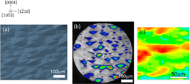
(a) four-faceted hillocks on m-plane GaN MOVPE sample, facet dependence of (b) leakage current and (c) PL peak intensity of the m-plane GaN Schottky barrier diode.
References
- 1 G. T. Dang, A. P. Zhang, F. Ren, X. A. Cao, S. J. Pearton, H. Cho, J. Han, J. I. Chyi, C. M. Lee, C. C. Chuo, S. N. George Chu, and R. G. Wilson, IEEE Trans. Electron Devices 47, 692 (2000).
- 2 Y. Yoshizumi, S. Hashimoto, T. Tanabe, and M. Kiyama, J. Cryst. Growth 298, 875 (2007).
- 3 K. Matocha, T. P. Chow, and R. J. Gutmann, IEEE Trans. Electron Devices 52, 6 (2005).
- 4
J. Kolnık,
İ. H. Oğuzman,
K. F. Brennan,
R. Wang, and
P. P. Ruden,
J. Appl. Phys.
81, 726
(2009).
10.1063/1.364213 Google Scholar
- 5
I. H. Oğuzman,
E. Bellotti,
K. F. Brennan,
J. Kolnı,
R. Wang,
P. P. Ruden,
E. Bellotti, and
K. F. Brennan,
J. Appl. Phys.
81, 7827
(2013).
10.1063/1.365392 Google Scholar
- 6 M. Himmerlich, A. Eisenhardt, S. Shokhovets, S. Krischok, J. Räthel, E. Speiser, M. D. Neumann, and N. Esser, Appl. Phys. Lett. 103, 171602 (2016).
- 7 K. Kunihiro, K. Kasahara, Y. Takahashi, and Y. Ohno, IEEE Electron Device Lett., 20, 608 (1999).
- 8 J. Suda, K. Yamaji, Y. Hayashi, T. Kimoto, K. Shimoyama, H. Namita, and S. Nagao, Appl. Phys. Exp. 3, 101003 (2010).
- 9 Z. Hu, K. Nomoto, B. Song, M. Zhu, M. Qi, M. X. Gao, V. Protasenko, D. Jena, and H. G. Xing, Appl. Phys. Lett. 107, 243501 (2015).
- 10 M. Qi, K. Nomoto, M. Zhu, Z. Hu, Y. Zhao, V. Protasenko, B. Song, G. Li, J. Verma, S. Bader, P. Fay, H. G. Xing, and D. Jena, Appl. Phys. Lett. 107, 232101 (2015).
- 11 T. Oikawa, Y. Saijo, S. Kato, T. Mishima, and T. Nakamura, Nucl. Instruments Methods Phys. 365, 168 (2015).
- 12 M. Naganawa, T. Aoki, T. Mishima, and K. Shiojima, Jpn. J. Appl. Phys. 55, 04EG06 (2016).
- 13 T. Fujiwara, S. Keller, M. Higashiwaki, J. S. Speck, S. P. DenBaars, and U. K. Mishra, Appl. Phys. Express 2, 061003 (2009).
- 14 T. Fujiwara, S. Rajan, S. Keller, M. Higashiwaki, J. S. Speck, S. P. DenBaars, and U. K. Mishra, Appl. Phys. Express 3, 011001 (2009).
- 15 R. M. Farrell, D. A. Haeger, X. Chen, C. S. Gallinat, R. W. Davis, M. Cornish, K. Fujito, S. Keller, S. P. Denbaars, S. Nakamura, and J. S. Speck, Appl. Phys. Lett. 96, 2319070 (2010).
- 16 A. Hirai, Z. Jia, M. C. Schmidt, R. M. Farrell, S. P. Denbaars, S. Nakamura, and J. S. Speck, Appl. Phys. Lett. 91, 191906 (2007).
- 17 C. Q. Chen, M. E. Gaevski, W. H. Sun, E. Kuokstis, J. P. Zhang, R. S. W. Fareed, H. M. Wang, J. W. Yang, G. Simin, M. A. Khan, H. P. Maruska, D. W. Hill, M. M. C. Chou, and B. Chai, Appl. Phys. Lett. 81, 3194 (2002).
- 18 M. Rudzinski, R. Kudrawiec, L. Janicki, J. Serafinczuk, R. Kucharski, M. Zajac, J. Misiewicz, R. Doradzinski, R. Dwilinski, and W. Strupinski, J. Cryst. Growth 328, 5 (2011).
- 19 K. M. Kelchner, L. Y. Kuritzky, S. Nakamura, S. P. Denbaars, and J. S. Speck, J. Cryst. Growth 411, 56 (2015).
- 20 A. S. Barker and M. Ilegems, Phys. Rev. B 7, 743 (1973).
- 21 A. M. Goodman, J. Appl. Phys. 34, 329 (1963).
- 22 M. Nakayama, H. Tanaka, M. Ando, and T. Uemura, Appl. Phys. Lett. 89, 031909 (2006).
- 23 H. P. D. Schenk, S. I. Borenstain, A. Berezin, A. Schön, E. Cheifetz, S. Khatsevich, and D. H. Rich, J. Appl. Phys. 103, 103502 (2016).