
Journal list menu

 Issue
Issuephysica status solidi (RRL) – Rapid Research Letters: Volume 16, Issue 12
December 2022
Export Citations
Download PDFs
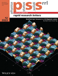
Cover Picture
Modified Spin Textures in a 3D Magnetic Lattice
- First Published: 30 November 2022
Modified Spin Textures
Three dimensional magnetic nanostructures exhibit many new properties and phenomena due to the extra degree of freedom compared to two dimensional nanostructures. In article number 2200213, Vivian Ng and Ba Myint create a magnetic lattice by overlapping hour-glass structures arrays on a 2D antidot matrix through a self-aligned nanosphere lithography technique. The field reversal behaviour and magnetic properties of the 3D magnetic lattice are characterized by magnetic force microscopy and the spin-curvature display unique magnetic behaviour as a consequence of the interplay of magnetic coupling.
Masthead
Review
15 years of pss RRL
Fabrication of Crystalline Si Thin Films for Photovoltaics
- First Published: 21 September 2022
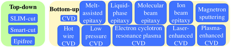
Crystalline Si thin films can be fabricated mainly via “top-down” and “bottom-up” approaches. The “top-down” approaches involve producing a fragile interfacial layer inside a crystalline Si substrate. In the “bottom-up” approaches, various epitaxial growth techniques allow to deposit thin crystalline Si films on a parent substrate. Both approaches require the transfer of the thin c-Si layer to a foreign substrate.
Research Articles
Modified Spin Textures in a 3D Magnetic Lattice
- First Published: 29 August 2022
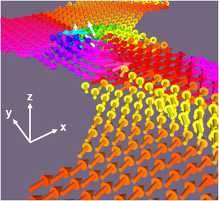
A 3D magnetic lattice created by stacking hour-glass structure (HGS) over a 2D antidot matrix is reported. The study shows how the magnetic spin texture of the 3D lattice along the hard axis is modified by the HGS via multivortices induced reversal process. A new method of comparing simulation and experimental results using a MATLAB divergence computation software is reported.
Tunable Optoelectronic Properties of Bilayer MoS2 via Interlayer Twist and Uniaxial Strain
- First Published: 26 August 2022
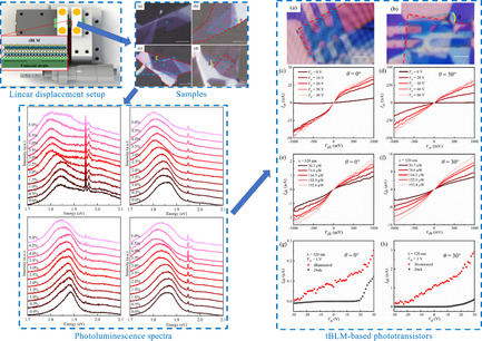
Herein, by applying a uniaxial strain up to 5%, the evolution of the Raman and photoluminescence spectra of bilayer MoS2 with four different twist angles is investigated. Further, the phototransistor based on the 30°-twisted structure is constructed. Its photoresponsivity (R) and specific photodetectivity (D*) are improved by ≈20 and ≈100 times than those values of the 0°-twisted one, respectively.
Investigation of the Electron–Phonon Coupling in Dirac Semimetal PdTe2 via Temperature-Dependent Raman Spectroscopy
- First Published: 01 September 2022
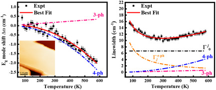
This study investigates the electron–phonon coupling and the phonon anharmonicity in Raman-active modes (E g and A 1g) in the exfoliated PdTe2 nanoflakes based on temperature-dependent Raman scattering. Both E g mode with a Gaussian lineshape and A 1g mode with a Fano line shape show nonlinear frequency redshift, linewidth broadening with temperature, revealing the different electron–phonon coupling constants.
Auxeticity and Its Pressure Dependence for Strongly Anisotropic Hard Cyclic Tetramers
- First Published: 25 August 2022
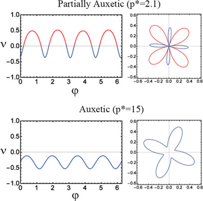
Auxetics are materials characterized by a negative Poisson's ratio. They increase their transverse dimensions under uniaxial tension and decrease them under compression. Depending on the pressure, the auxetic and partially auxetic behavior of strongly anisotropic hard cyclic tetramers is shown. The crystalline phase of tetramers becomes partially auxetic below the pressure and offers completely auxetic behavior above that pressure.
The High Photoresponse of Stress-Tuned MoTe2 Optoelectronic Devices in the Telecommunication Band
- First Published: 13 August 2022
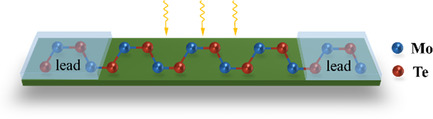
The linear photoelectric effect (PGE) phenomenon of devices composed of noncentral inversion symmetric monolayer MoTe2 is investigated. The PGE photocurrent can be greatly enhanced by biaxial tensile stress and external bias voltage, and the high photoresponse can be tuned to the telecommunication band range. This work demonstrates further applications of MoTe2 monolayer devices in integrated photonics.
Self-Trapped Exciton States in Metal Halide Perovskites van der Waals Heterostructures
- First Published: 13 August 2022
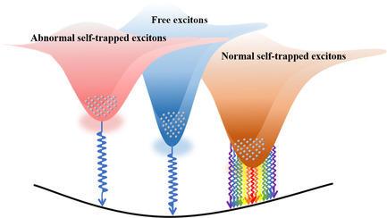
Self-trapped excitons (STEs) are studied in 2D metal halide perovskite (MHP) van der Waals (vdW) heterojunctions based on the improved Pollmann–Büttner model, in which these exciton states are classified into the normal and abnormal STEs according to the magnitude of the correction of exciton binding energy.
The Magnetic Phase Transition of FeRh Modulated by AC Magnetic Field
- First Published: 02 August 2022
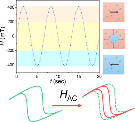
Under the alternating current magnetic field, the phase transition of the ferromagnetic (FM) to antiferromagnetic (AFM) is promoted and the heating branch shifts at a rate of −8 K T−1, which causes the thermal hysteresis of FeRh reduction of about 2 K. These phenomena may be attributed to the Zeeman energy and the periodic vibration of domain walls. This work provides a method for reduction of the thermal hysteresis of phase transition materials.
Electronic State Coupling Between Structural Deformation and Surficial Defects in Co-Layered LaCoSi for Hydrogen Evolution Reaction
- First Published: 19 August 2022
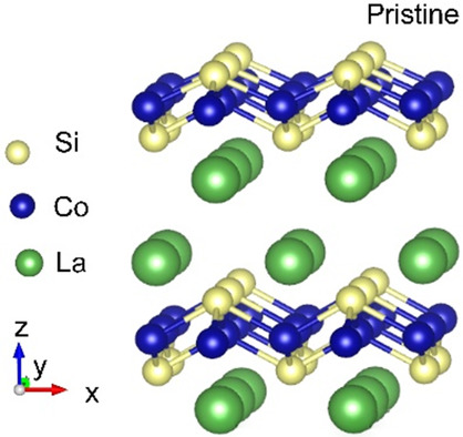
The proposed Co-layered LaCoSi material discloses the electronic state coupling between structural strain and defect distribution, where the bonding interaction between reactants and catalysts can be affected by the electronic reconfiguration at reactive sites. The catalytic activity of Co site is obviously enhanced by tensile strain, and the antibonding interaction between Co and adsorbed hydrogen is also enforced.
Photoluminescence Dynamics of MAPI Perovskite Films Induced by Lateral Electric Field
- First Published: 31 August 2022
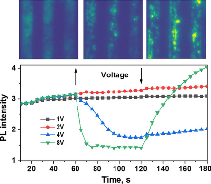
Voltage applied in the lateral configuration to the MAPI perovskite film formed between platinum electrodes causes a complex sequence of processes observed such as photoluminescence quenching, appearance of unstable contrastive pattern, and increase in its intensity after voltage termination. This behavior is explained by the variation of the spatial electric field strength distribution and by the formation of temporal luminescence quenchers.
Resistive Switching Characteristics of Fullerene (C60) in Polymannose Thin Film
- First Published: 10 September 2022
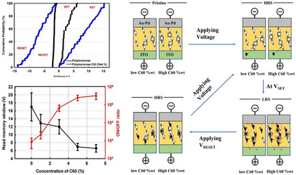
Herein, comparison of resistive switching characteristics of polymannose-based thin film with (1–7 wt%) and without fullerene (C60) is presented. Endurance of devices with C60 in polymannose is better than without C60. Memory window and ON/OFF ratio are, respectively, reduced and increased as the concentration of C60 increases as it serves as interlock between molecular chains of polymannose.
Long-Term Field Screening by Mobile Ions in Thick Metal Halide Perovskites: Understanding Saturation Currents
- First Published: 06 September 2022
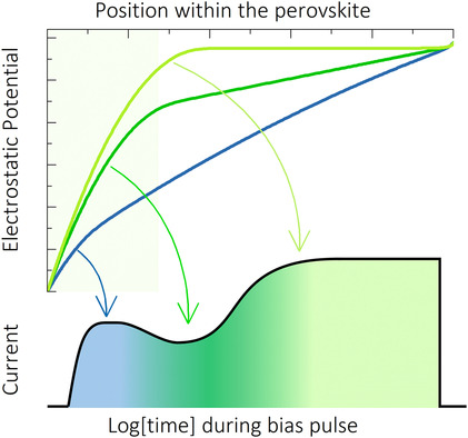
The mobile ion-mediated electric field screening processes defining the current regimes along polarization times up to tens of hours are described for millimeter-thick perovskites via drift-diffusion numeric simulations.
Quantitative Calculation of the Clustering Behavior of Fe-Rich and Cr-Rich REFepCr1−pO3 Crystals
- First Published: 10 September 2022
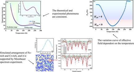
This work determines the first calculation of the cluster state of the perovskite REFe1−xCrxO3 system based on magnetic calculations using molecular field theory, using GdFe0.5Cr0.5O3 as an example, and the calculations show that the system has some Fe- and Cr-rich cluster behavior. The calculated results are verified by the Mossbauer spectra.
Multiple Second-Order Topological Photonic Systems for Multichannel Beam Splitting and Wavelength Demultiplexing
- First Published: 14 September 2022
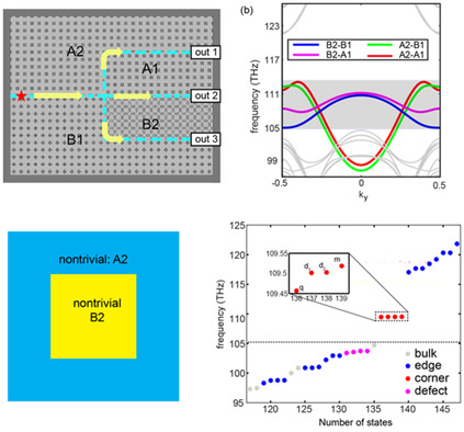
Under continuous transformation, conventional topologically nontrivial square lattice unit cell can be turned into another nontrivial one, enabling to construct multiple topological photonic systems with their trivial counterparts. With such systems, one can not only realize multichannel beam splitting for edge states, but also obtain both spatially and spectrally separated corner states.
Stitching-Induced Structural Corrugation of Twisted Grain Boundaries in CVD-Grown MoS2 Domains
- First Published: 21 September 2022
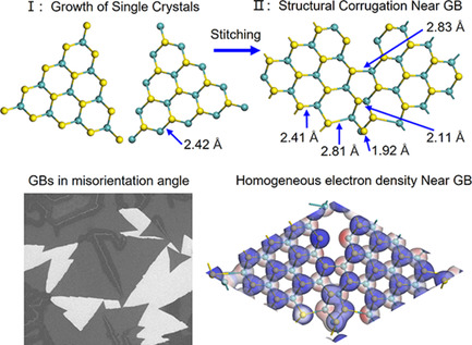
A set of microscopies and spectroscopies complemented with theoretical calculations consistently show that the mechanical and electrostatic properties near the grain boundary (GB) of chemical vapor deposition (CVD)-grown MoS2 are distinct from the interior ones. The underlying mechanism is proposed to be that the edge stitching behavior of MoS2 with a misorientation angle leads to structural corrugation due to lattice deformation.
Effect of Strain on the Lattice Thermal Conductivity in SrTiO3 from First-Principles Calculations
- First Published: 21 September 2022

The self-consistent phonon theory is used in the calculation of lattice thermal conductivities in strained and unstrained SrTiO3. The lattice thermal conductivity of SrTiO3 decreases by less than 20% under in-plane compressive or tensile strain. Intrinsic phonon scattering alone is unable to cause a large decrease of thermal conductivity up to 60% observed in the experiment.
The Dissociation of Gallium–Hydrogen Pairs in Crystalline Silicon during Illuminated Annealing
- First Published: 20 September 2022

The reaction behavior of hydrogen may be the key to understand light- and elevated temperature-induced degradation in silicon solar cells. The authors describe one aspect of its behavior, the gallium–hydrogen pair formation and subsequent dissociation phenomena, under varying injection and temperatures. The results may serve as a tool for hydrogen quantification in Ga-doped Si-wafers.
Hexagonal Al2O3/TiO2/TiN Nanotubes-Based Sensor for CO2 Detection
- First Published: 27 September 2022
Hexagonal Al2O3/TiO2/TiN nanotube sensor is investigated using Al2O3 template, the Ni imprinting and two-step anodization technique, as well as atomic layer deposition and DC sputtering techniques, are used. This work offers insights into the sensitivity of the sensor, which is increased from 3.2% to 16.4%, also a great response and recovery times of 3 and 35 s.
Electronic Behavior of GaN Nanowire Photocathode Surface Coated with n-Type GaN Capping Layer via First Principles
- First Published: 27 September 2022
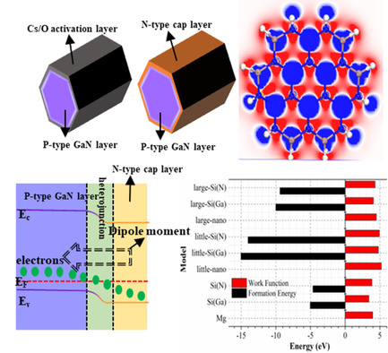
GaN nanowires with n-type capping layers are investigated. Si atoms are more likely to substitute Ga atoms to form an n-type capping layer. n-Type capping layer reduces the work function of the GaN material. The addition of Si atoms increases the possibility of charge transfer. Si atoms provide shallow donor energy level in the n-type GaN capping layer.
Sign up for email alerts
Tools
![]()
In 2022, the youngest family member physica status solidi (RRL) – Rapid Research Letters is turning 15 years. To celebrate this milestone, we present a new virtual collection with invited articles.
![]()
As we celebrate the 60th anniversary year of the physica status solidi family, click here to access our continuously updated collection of invited articles written by authors and partners of the pss journals.