Journal list menu

 Issue
Issuephysica status solidi (a): Volume 217, Issue 24
December 2020
Export Citations
Download PDFs
Cover Picture
Effect of Zr Addition on Threshold Switching Characteristics of Amorphous Ga2Te3 Thin Films
- First Published: 18 December 2020
Ovonic Threshold Switching
The modulation of ovonic threshold switching (OTS) characteristics is required in a cross-point array structure. Therefore, the effect of Zr doping on the amorphous Ga2Te3 having OTS characteristics is examined. Consequently, the thermal stability of the Zr-doped Ga2Te3 is improved and the threshold and holding voltages are increased with the increasing Zr doping concentration. More details can be found in article number 2000623 by Hyunchul Sohn and co-workers.
Masthead
Original Papers
Effect of Zr Addition on Threshold Switching Characteristics of Amorphous Ga2Te3 Thin Films
- First Published: 23 October 2020
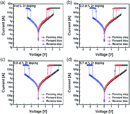
The effect of Zr doping on the amorphous Ga2Te3 is examined in this work. The optical and electrical properties and the thermal stability of Zr-doped Ga2Te3 thin films are analyzed. Consequently, the thermal stability of the Zr-doped Ga2Te3 thin film is improved, and the threshold and holding voltages are increased with the increasing Zr doping concentration.
Intense Anti-Stokes Emission from Erbium Ions in Gallium Lanthanum Sulphide–Oxide Glass in the Visible Spectral Range
- First Published: 21 October 2020
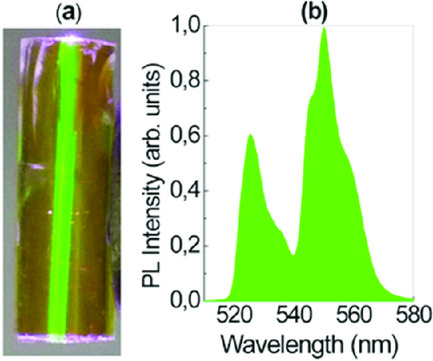
Photoluminescence spectra is investigated in erbium-doped GaLaS(O) glass under 808 nm excitation. Herein, the visual impression and green coloration of photoluminescence (PL) are shown. The length of the cylinder is 10 mm and the diameter is close to 3 mm. The excitation laser beam passes along the axis of the cylinder and causes the intense up-conversion.
Study of Dislocations in Homoepitaxially and Heteroepitaxially Grown AlN Layers
- First Published: 16 October 2020
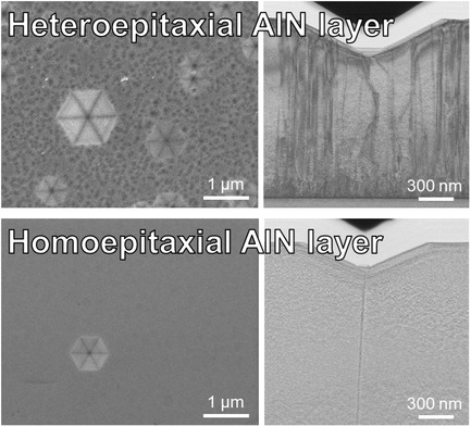
The types and their densities of the dislocations in heteroepitaxially and homoepitaxially grown AlN layers are investigated by the formation of etch pits by wet chemical etching. With this method, it is possible to accurately evaluate the dislocation density of high-quality AlN layers (dislocation density < 104 cm−2), which is difficult to evaluate by conventional methods.
Laser Ablation and Ni/Cu Plating Approach for Tunnel Oxide Passivated Contacts Solar Cells with Variate Polysilicon Layer Thickness: Gains and Possibilities in Comparison to Screen Printing
- First Published: 21 October 2020
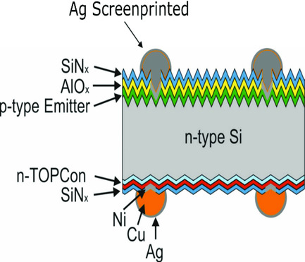
Latest investigation of laser interaction on passivated contact devices such as TOPCon, to form nickel/copper plated contacts, reveal interesting findings. With optimized wavelength and pulse duration, damage from laser is kept highly superficial and is reversible by thermal annealing process. This allows reducing the polysilicon thickness, thereby decreasing production costs and also enables an efficiency gain of 1% (absolute).
Sputtering Power and Annealing Effects on the Properties of Zn2SnO4–SnO2 Composite Thin Film for Pungent Smelling Gas (NH3) Detection
- First Published: 20 October 2020
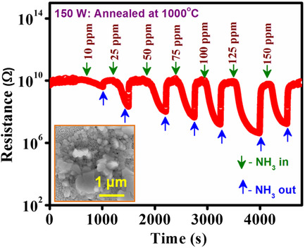
Zn2SnO4–SnO2 composite thin films are prepared by radio frequency magnetron sputtering technique using the homemade Zn2SnO4–SnO2 sputtering target. The film deposited with 150 W and annealed at 1000 °C exhibits an excellent sensing response of 1897 toward NH3 gas at room-temperature working condition with a good response and recovery time.
Preparation of Bi-Doped ZnO Thin Film over Optical Fiber and Their Application as Detection of Ethylenediamine in an Aqueous Medium Based on the Evanescent Field Technique
- First Published: 10 November 2020
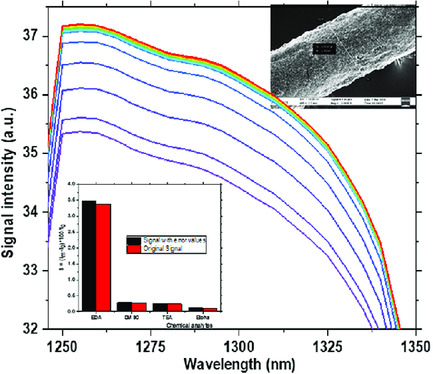
The 6 wt% Bi-doped ZnO thin-film based over optical fiber sensor is reported. Thin-film over modified clad fiber keeping thickness within the 2–5 μm with an optimized penetration depth of 8.939 μm exhibit promising behavior towards ethylenediamine with sensitivity (%) 3.843, the response time (15 s), and recovery time (≈5 min).
Energy Storage Properties of Mn and Y Codoped Ba0.67Sr0.33TiO3 Ceramics
- First Published: 21 November 2020
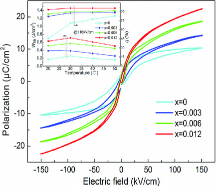
Ba0.67–xYxSr0.33Ti0.995Mn0.005O3 (BSTM-xY, x = 0, 0.003, 0.006, and 0.012) ceramics are synthesized by citrate–nitrate combustion methods. The introduction of Y enhances the energy storage properties, dielectric properties, and leakage current density of BSTM-xY ceramics. The energy efficiency presents good thermal stability and electric field stability as Y doping.
Improving CdTe-Based Thin-Film Solar Cell Efficiency with the Oxygenated CdSe Layer Prepared by Sputtering Process
- First Published: 13 November 2020
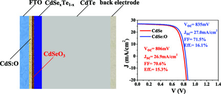
Oxygenated cadmium selenide (CdSe:O) is prepared by the sputtering process. The incorporation of oxygen into the sputtering atmosphere promotes the formation of CdSeO3 phase. When applied as the window layer, the CdSe:O can improve the performance of CdTe-based thin-film solar cell. Both open-circuit voltage (Voc) and fill factor (FF) are improved due to the formation of CdSeO3.
Nd3+-Doped Lead Boro Selenate Glass: A New Efficient System for Near-Infrared 1.06 μm Laser Emission
- First Published: 24 October 2020
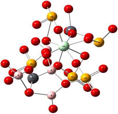
Herein, a structural fragment of PbO–B2O3–SeO2:Nd2O3 glass network is illustrated. The Nd3+ coordination number is taken as 8 based on the band position of 4I9/2→2P1/2 transition in the absorption spectrum. The Se ions are shown in (SeO3)2− and (SeO4)2− structural units. BO3, BO4, and PbO4 units are also shown in the fragment.
Characterization of Ultrathin Fully Depleted Silicon-on-Insulator Devices Using Subthreshold Slope Method
- First Published: 06 November 2020
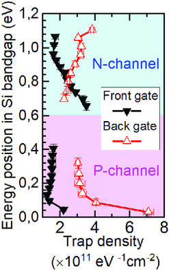
Measurements of subthreshold swing in a fully depleted silicon-on-insulator high-k dielectric-metal gate field-effect transistor (FET) at several temperatures (namely, in the range 120–400 K) allows determination of interface trap density distributions at the front and back gate interfaces. Combining results for N- and P-channel FET one can obtain the trap density distributions in almost the entire Si-channel bandgap.
Sign up for email alerts
Tools
![]()
In 2022, the youngest family member physica status solidi (RRL) – Rapid Research Letters is turning 15 years. To celebrate this milestone, we present a new virtual collection with invited articles.
![]()
As we celebrate the 60th anniversary year of the physica status solidi family, click here to access our continuously updated collection of invited articles written by authors and partners of the pss journals.