Journal list menu

 Issue
Issuephysica status solidi (a): Volume 215, Issue 10
Special Issue:Nitride Semiconductors
May 23, 2018
Export Citations
Download PDFs
Cover Picture
Improved Light Output Power of 16 × 16 Pixelated Micro-LEDs for Headlights by Enhancing the Reflectivity and Coverage of the p-Electrode (Phys. Status Solidi A 10∕2018)
- First Published: 23 May 2018

Light Emitting Diodes
A pixel array of GaN-based micro-light emitting diodes (μ-LEDs) based on a flip-chip structure and driven by a passive matrix is fabricated. The light output power of 16 × 16 pixelated μ-LEDs for headlights of vehicles is greatly improved by enhancing the reflectivity and coverage of the p-electrode. More details can be found in article number 1700571 by Joon Seop Kwak and co-workers
Masthead
Editor's Choice
Laser Diodes
Watt-Class Green (530 nm) and Blue (465 nm) Laser Diodes
- First Published: 05 December 2017

High-power and high-efficiency green and blue laser diodes are successfully fabricated on semipolar  plane and conventional c-plane GaN substrates, respectively. These lasers are promising light sources that meet the ITU-R Recommendation BT.2020 for future laser display applications.
Optical Guiding
A GaN-Based VCSEL with a Convex Structure for Optical Guiding
- First Published: 20 February 2018

A GaN-based vertical-cavity surface-emitting laser (VCSEL) formed with a spacer layer is designed and fabricated. The convex structure with a 15-nm step between center and peripheral area could result in a relative refractive index difference of 1.5%. Room-temperature continuous-wave operation of the VCSEL is demonstrated, showing a lower threshold current and a multi-mode operation. Thus, the convex structure for optical guiding plays an important role in the development of high-performance GaN-based VCSELs.
Original Papers
Light Emitting Diodes
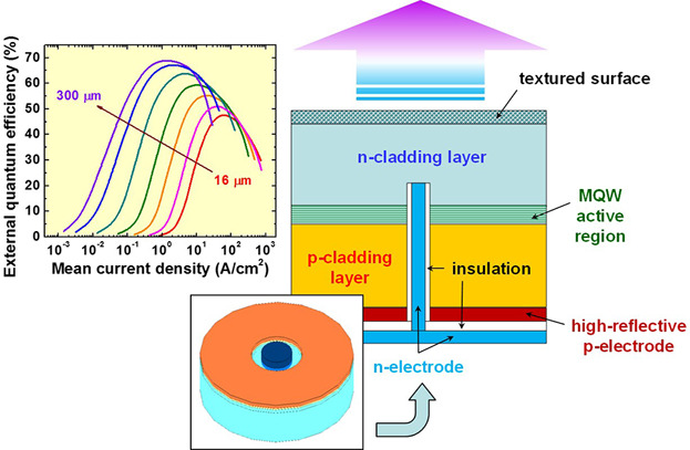
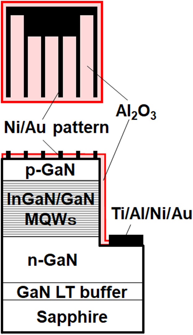
Improved Light Output Power of 16 × 16 Pixelated Micro-LEDs for Headlights by Enhancing the Reflectivity and Coverage of the p-Electrode
- First Published: 10 January 2018

A pixel array of micro-light emitting diodes (μ-LEDs) based on a flip-chip structure and driven by a passive matrix is fabricated. The array is fabricated through multilevel metallization using a photosensitive polyimide inter-metal dielectric layer. The high reflectivity and large coverage of the p-type reflective electrode is essential to enhance the light output power of the μ-LED array.
Interfacial Protection Layer
Bias Temperature Instability of Normally-Off GaN MIS-FET with Low-Pressure Chemical Vapor Deposition SiNx Gate Dielectric
- First Published: 10 January 2018
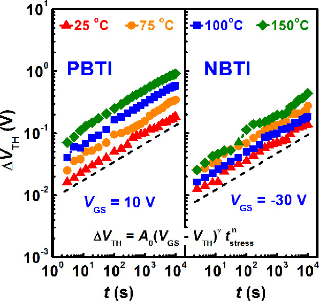
Bias temperature instability (BTI) and related mechanisms are investigated in the E-mode GaN MIS-FET with LPCVD-SiNx gate dielectric. Improved VTH stability is obtained with PECVD-SiNx interface protection layer, benefiting from the reduced trap density at/near the SiNx/GaN interface. Combining the BTI tests and drain current 1/f noise analysis, we ascribe the VTH instability to the trapping/detrapping of the pre-existing trap states located at SiNx/GaN interface and/or in the gate dielectric.
High Electron Mobility Transistors
High-Performance E-Mode AlGaN/GaN MIS-HEMT with Dual Gate Insulator Employing SiON and HfON
- First Published: 14 November 2017

A high-performance E-mode AlGaN/GaN MIS-HEMTs is fabricated with atomic layer deposited 5 nm SiON/16 nm HfON. Plasma nitridation is employed in every atomic layer deposition cycle to deposit SiON and HfON dielectrics. SiON is used as an interfacial layer to ensure a high-quality AlGaN/dielectric interface, and high-k HfON is employed to realize a large transconductance, a high on-state current, and a high on/off current ratio.
Hot Electron Transistors
Fabrication and Characterization of Graphene Heterostructures with Nitride Semiconductors for High Frequency Vertical Transistors
- First Published: 13 November 2017
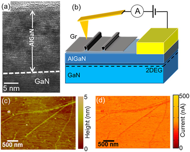
High resolution structural, morphological and electrical characterization of a graphene junction with an AlGaN/GaN heterostructure. An optimized graphene transfer procedure results in a uniform graphene coverage of the AlGaN surface. The impact of graphene wrinkles on the electrical properties of the heterojunction is investigated by conductive AFM.
Depletion Enhancement Effect
The Recessed Trapezoidal Groove Dual-Gate AlGaN/GaN E-Mode Transistor by Using Depletion Enhancement Effect
- First Published: 23 January 2018
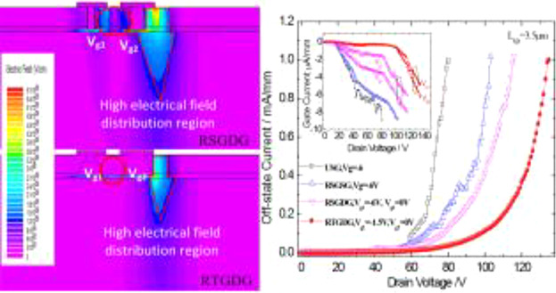
An attractive feature of the recessed trapezoidal groove dual-gate (RTGDG) E-mode AlGaN/GaN HEMT is the capability to decrease the gate leakage and off-state leakage. Such low off-state leakage, high breakdown voltage, and high frequency enable this kind of GaN-based E-mode transistor very promising for high voltage drive circuit, low power, and high speed circuit applications.
Recess Surfaces
Improvement of Channel Mobility of GaN-MOSFETs With Thermal Treatment for Recess Surface
- First Published: 19 December 2017
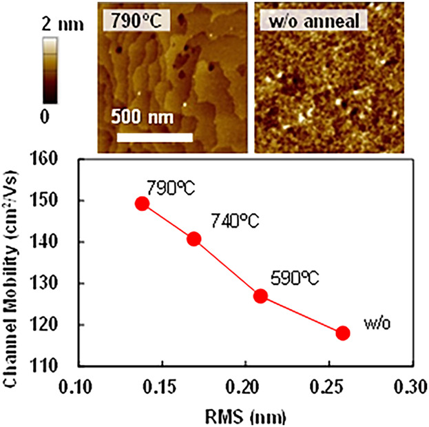
In this paper, thermal treatment technique under NH3 ambient for the recess surface of GaN-MOSFETs in order to remove plasma-induced damage is demonstrated. Atomically flat interface between SiO2 and GaN at the recessed-gate and improved channel mobility of the MOSFETs are achieved utilizing the thermal treatment under appropriate temperature and NH3 partial pressure.
Light Emitting Diodes
Vertical-Type Blue Light Emitting Diode by Mixed-Source Hydride Vapor Phase Epitaxy Method
- First Published: 14 November 2017

Schematic drawing of the vertical blue LED chip grown by a mixed-source HVPE with multi-sliding boat system.
Quantum Dots
Large Area Polymer Composite Films Embedded with Colloidal Quantum Dots for Efficient White Light Generation
- First Published: 14 November 2017
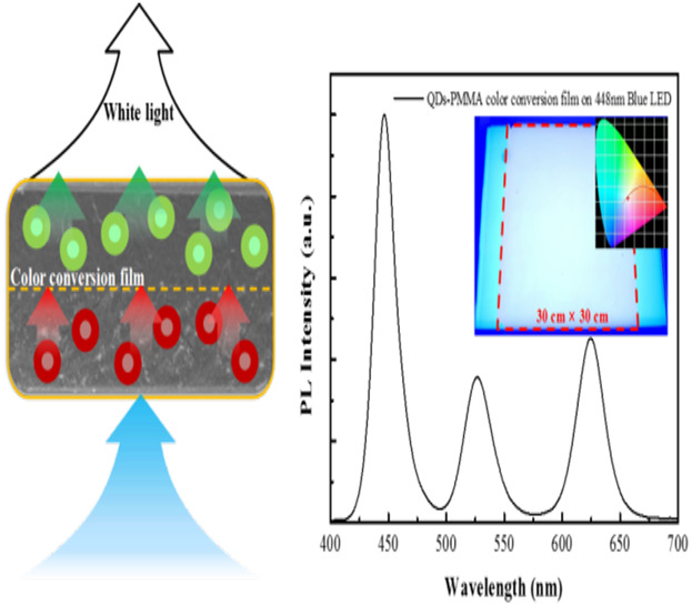
The colloidal quantum dots (QDs) embedded in polymer matrix agglomerate. When the distance between QDs becomes within several nanometers, an energy transfer without light emission occurs from small QD to large QD. To avoid this nonradiative energy transfer causing a significant redshift from the desired final color, a double layer polymer structure comprised of separated green and red emitting composite film is fabricated.
Light-Emitting Diodes
Study on the Main-Chain Structure of Amorphous Fluorine Resins for Encapsulating AlGaN-Based DUV-LEDs
- First Published: 08 January 2018
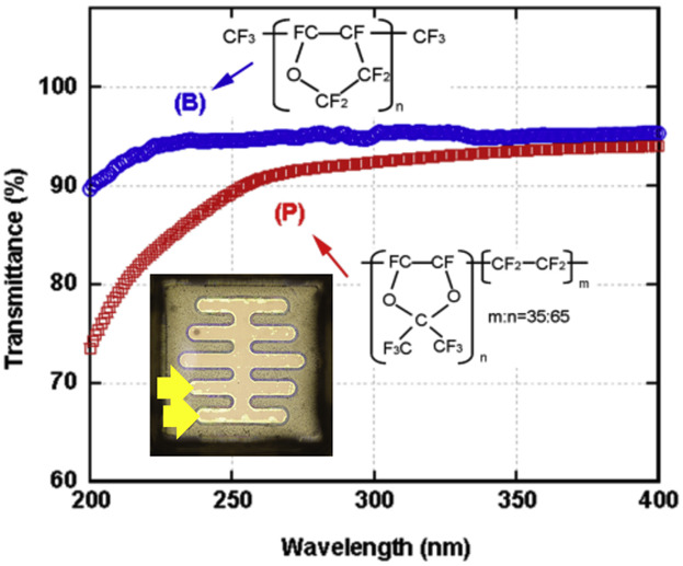
The molecular structure of fluorine resins with transmittance in DUV for encapsulating DUV-LEDs is clarified. The fluorine polymer incorporating (COCOC) rings caused the electrodes damage, resulting in device fault. The resin with the main chain of (CCCOC) terminated with CF3 ends is considered to guarantee no damage to the devices.
A Comparative Study of GaN-Based Direct Current and Alternating Current High Voltage Light-Emitting Diodes
- First Published: 29 January 2018
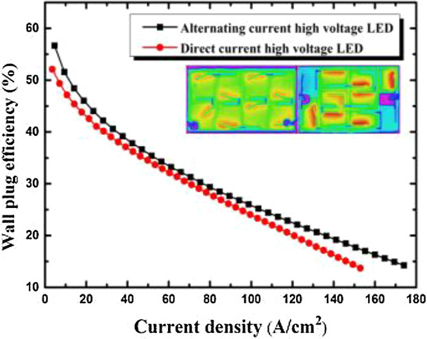
In this work, optical and electrical characteristics of direct current high voltage LEDs (DC-HV LEDs) and alternating current high voltage LEDs (AC-HV LEDs) are compared. The AC-HV LED has a relatively larger wall-plug efficiency than DC-HV LED over a specific current density range. It is found that light output power of AC-HV LEDs is dependent on both the number of working cells and the ratio of radiation area to total chip area.
From Large-Size to Micro-LEDs: Scaling Trends Revealed by Modeling
- First Published: 11 December 2017
Using selfconsistentelectrical-thermal-optical simulations, this paper analyzes general trends in variation of main light-emitting diode's (LED) characteristics under wide-range scaling of the device dimensions. Surface recombination at the open edges of LED active region, Auger recombination initiated by high electron and hole density in the active region, and temperature dependence of recombination coefficients are found to be the major factors controlling the LED efficiency. The revealed scaling trends are interpreted qualitatively in terms of a simple ABC-model, though quantitative predictions require elaborated numerical modeling.
Solar Cells
A Comparative Study of InGaN/GaN Multiple-Quantum-Well Solar Cells Grown on Sapphire and AlN Template by Metalorganic Chemical Vapor Deposition
- First Published: 06 December 2017
In this paper the influence of the lattice strain in InGaN/GaN multiple-quantum-well solar cells on their performance by comparing the samples grown on sapphire and on AlN/sapphire template by metalorganic chemical vapor deposition is discussed. The experimental results indicate that a large compressive strain deteriorates the device performance owing to the generation of nonradiative recombination centers.
Quantum Well Solar Cells
Study of InGaN/GaN Multiple Quantum Well Solar Cells With Different Barrier Thicknesses
- First Published: 13 November 2017
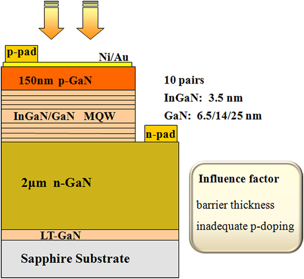
The influence of barrier thickness on the performance of InGaN/GaN multiple quantum well solar cells is investigated, showing that the thinner barrier favors the transport of photogenerated carriers but may be accompanied by larger leakage current. In addition, the detrimental effects of inadequate p-type doping and induced polarization field on the carrier collection are analyzed.
Deep-UV Light Emitting Diodes
Efficiency Improvement of Deep-Ultraviolet Light Emitting Diodes with Gradient Electron Blocking Layers
- First Published: 24 November 2017
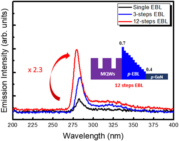
To improve the performance of deep-UV light emitting diodes (DUV-LEDs), the gradient electron blocking layers (GEBLs) are introduced. DUV-LED structures with different GEBLs are grown by high-temperature MOCVD. The electroluminescence intensity of the LED with 12-step EBL is approximately 2.3 times that of LED with single EBL at 280 nm. Also, all simulation data support the effect of a GEBL on DUV-LEDs.
Light-Emitting Diodes
Effect of the GaN:Mg Contact Layer on the Light-Output and Current-Voltage Characteristic of UVB LEDs
- First Published: 11 December 2017

In order to realize UVB light emitting diodes (LEDs) with high wall-plug efficiencies, the light extraction efficiency from the LED heterostructure must be maximized and operating voltages reduced. In this study, we investigate the effect of the GaN:Mg con-tact layer thickness on the light-output and current-voltage characteristics of UVB LEDs.
AlGaN Light-Emitting Diodes on AlN Substrates Emitting at 230 nm
- First Published: 20 December 2017
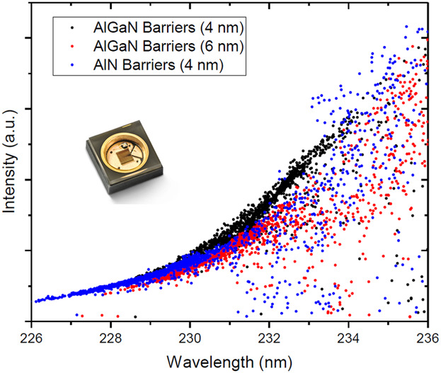
In this work UVC LEDs with emitting wavelengths as low as 230 nm and packaged powers averaging 0.1 mW are demonstrated. The shift in emission polarization across the wavelength region is displayed as a continuous function via photoluminescence. The lowest forward voltages to date at these wavelengths are achieved, and power output over time is investigated to demonstrate commercial feasibility.
Light Emitting Diodes
New Field Effect Deep-UV μLEDs Development
- First Published: 15 May 2018

This paper presents a new concept of deep-UV LED to overcome the doping issue of p-AlGaN. By adding a gate on the sidewall of the p-layer and the active area, the simulated wall plug efficiency of the structure is increased by a factor of 3 at a 3V lower working voltage.
Sign up for email alerts
Tools
![]()
In 2022, the youngest family member physica status solidi (RRL) – Rapid Research Letters is turning 15 years. To celebrate this milestone, we present a new virtual collection with invited articles.
![]()
As we celebrate the 60th anniversary year of the physica status solidi family, click here to access our continuously updated collection of invited articles written by authors and partners of the pss journals.