

Journal list menu

 Issue
IssueInternational Journal of Circuit Theory and Applications: Volume 52, Issue 10
4859-5435October 2024
Export Citations
Download PDFs
ISSUE INFORMATION
ORIGINAL ARTICLE
Analysis of super-source-follower-based GHz-bandwidth biquadratic low-pass filters
- Pages: 4859-4877
- First Published: 24 March 2024
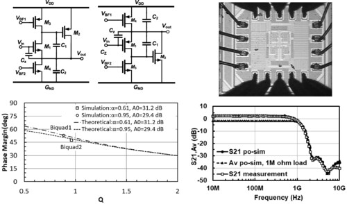
The relationship between the Q factor and the phase margin of the GHz-bandwidth super-source-follower-based low-pass filters is revealed. A 4th-order low-pass filter is then implemented using 90-nm CMOS technology, and the filter delivers a bandwidth of 1.3 GHz, P1dB of −11.94 dBm, and IIP3 of −4.5 dBm.
Comprehensive study of Class--E/F2 and inverse Class--F power amplifiers for mm-Wave systems utilizing 130 nm CMOS process
- Pages: 4878-4902
- First Published: 02 April 2024

This paper presents a comprehensive study of Class-E/F2 and inverse Class-F Power Amplifiers (PAs) designed for 35-42 GHz millimeter-wave applications, utilizing a 130 nm CMOS process with a comprehensive study and analysis of the limiting factors in the amplifier efficiency. The first proposed power amplifier is based on the class-E/F2 architecture, comprising a parallel capacitor, second harmonic resonance circuit, and output matching network while the second suggested power amplifier is constructed using the inverse class-F topology, which includes harmonic termination and matching networks. The harmonic termination circuit incorporates a second harmonic resonance network and utilizes a parasitic capacitor to control the harmonic components. Both the proposed class-E/F2 and inverse class-F architectures are employed to reshape the drain current and voltage waveforms, aiming to reduce the overlap between them and, consequently, improve efficiency.
Analysis and design of voltage-source parallel resonant class E frequency multiplier
- Pages: 4903-4917
- First Published: 22 March 2024
A new type of class E multiplier, that is, voltage-source parallel resonant class E multiplier, is proposed and designed. And the detailed analysis process is given. This new type of multiplier can operate with soft-switching conditions without DC-feed inductance or DC block capacitance. Two resonant filters are applied to decrease the harmonic components in the output voltage. The transistor voltage stress and circuit volume decreased greatly. The output power is much greater than in previous work. The voltage-source parallel resonant class E multiplier is more suitable for applications.
Design of a mixed load-modulation balanced power amplifier with ultra-extended power back-off range
- Pages: 4918-4938
- First Published: 19 March 2024
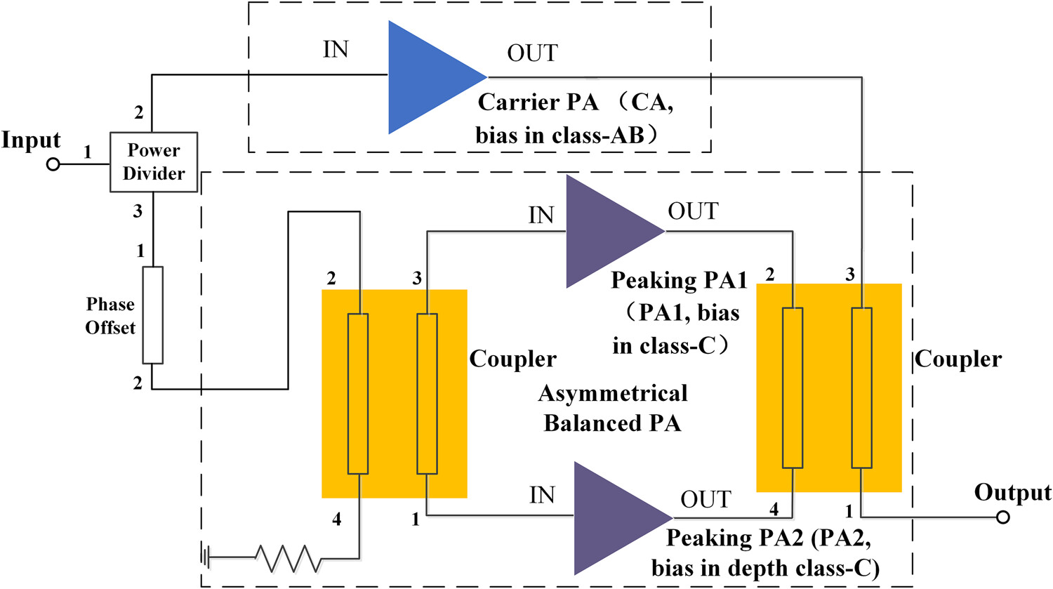
The pseudo-Doherty load-modulation balanced power amplifier (LMBA) consists of an asymmetric LMBA configuration and an asymmetrical coupler, thus greatly expanding the OBO. An LMBA with an OBO of 15 dB operating across 3.4–3.6 GHz is realized. The LMBA implemented here shows state-of-the-art performance in terms of the OBO range.
Modified elliptic response bandpass filtering integrated high-efficiency GaN MMIC power amplifier at 24–28 GHz
- Pages: 4939-4953
- First Published: 28 March 2024
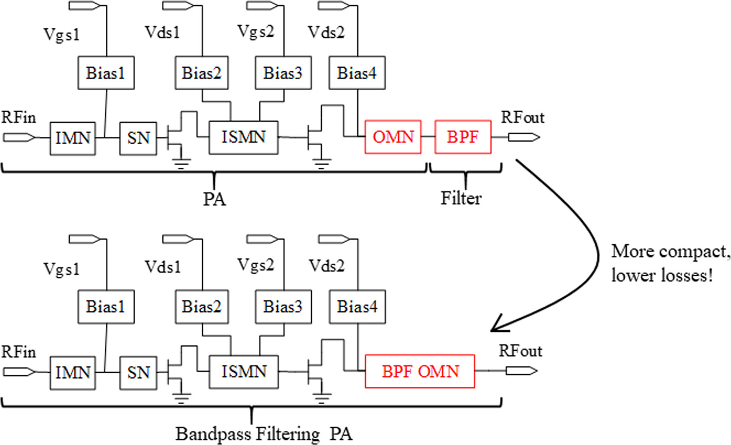
The co-design of power amplifiers (PA) and filter. PAs are often followed by filters to provide the out-of-band rejection and thus improve the signal-to-noise ratio. However, due to the limitation on the antenna element spacing, this configuration is too large in system and the interconnections have a high insertion loss. So, integrating the functionality of filtering response into the PAs is a more compact and lower loss scheme.
A detailed study of the current-reuse VCO's operation and a simple circuit technique to generate intrinsic-balanced outputs
- Pages: 4954-4969
- First Published: 15 March 2024
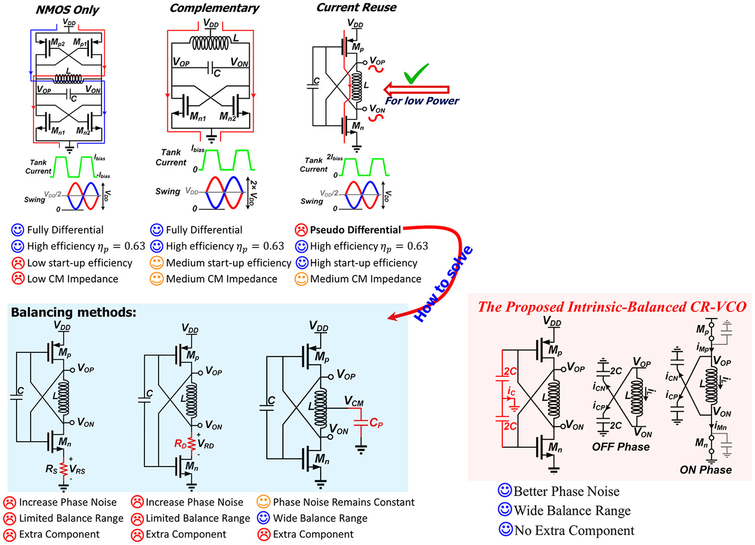
- This paper evaluates popular methods for balancing CR-VCOs' outputs.
- It assesses the effectiveness of those methods in terms of mismatch cancellation, PVT robustness, and phase noise.
- This work proposes a CR-VCO with inherent ability to generate balanced outputs. It is achieved by implementing single-ended tank capacitors to shunt the common-mode voltage to a real ground.
0.6-V CMOS bulk-driven instrumentation amplifier for IoMT bioimpedance analysis
- Pages: 4970-4984
- First Published: 07 March 2024
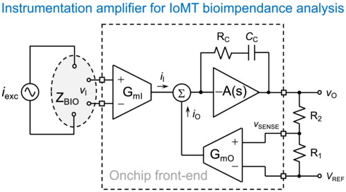
An instrumentation amplifier aimed at wideband bioimpedance analysis in the low-voltage low-power scenario of internet of medical things and supplied with 0.6 V is presented. Experimental results in 180 nm CMOS technology are provided.
An economical and simple strategy for overcoming the Hall sensor faults in three phase brushless DC motor drive
- Pages: 4985-5009
- First Published: 19 March 2024
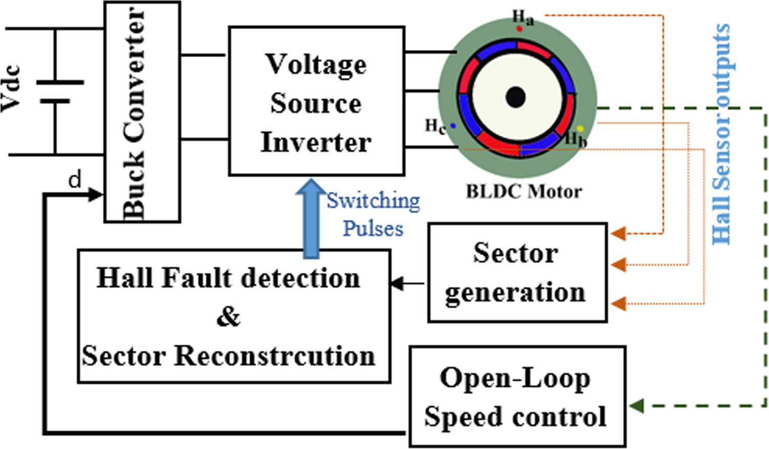
Hall sensors produce an output after every sixty degrees of rotation of the rotor, generating six sequences (called sector here) in one electrical cycle. Based on this sector information in each electrical cycle, a simple detection strategy for the Hall sensor fault is proposed. A pseudo-Hall sensor signal is generated from the healthy Hall sensor signal to reconstruct the faulty signal/s.
Positive-to-negative tunable delay circuit designed with NGD RC network
- Pages: 5010-5024
- First Published: 15 March 2024
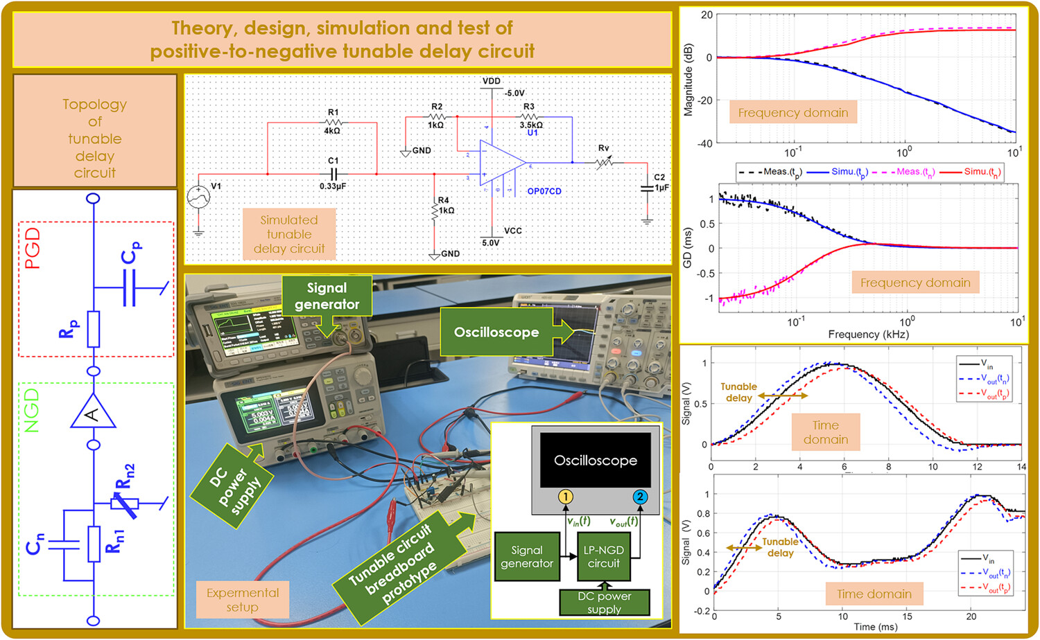
This paper presents an innovative study on theoretical design and test methodology of circuit exhibiting positive to negative tunable delay by using unfamiliar NGD topology.
An adaptive load-matching method for the induction heating coil with DC power supply
- Pages: 5025-5041
- First Published: 06 March 2024
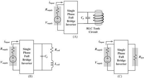
This article proposes to transfer maximum power from a power supply to an induction heating load by matching the dynamic resistance of the induction heating resonant circuit with the internal resistance of the power supply source, as shown in Figure (A). The proposed method includes selecting a capacitor CP, as shown in Figure (B), connected in parallel to the induction coil and tuning the correct value of the inverter frequency to the induction heating circuit resonant frequency. At resonance (Figure C), maximum power is transferred when the dynamic resistance of the resonant circuit is equal to the internal resistance of the DC power supply.
Characteristic parameter model and circuit-level simulation of gate-controlled dual direction SCR for on-chip ESD protection
- Pages: 5042-5056
- First Published: 12 March 2024
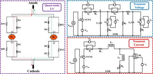
This paper proposes a novel behavioral model of GDDSCR device, which enables simulation of the bidirectional discharge path and snapback characteristics of ESD devices. The model parameters can be directly extracted from TLP tests, making it easy to apply to DDSCR devices. Experimental results demonstrate that the behavior model accurately reproduces the quasi-static IV characteristics with a good fit to the measured TLP IV characteristics.
Second harmonic reduction strategy for two-stage inverter energy storage system with dual active bridge converter based on virtual LC series resonant circuit
- Pages: 5057-5073
- First Published: 19 March 2024
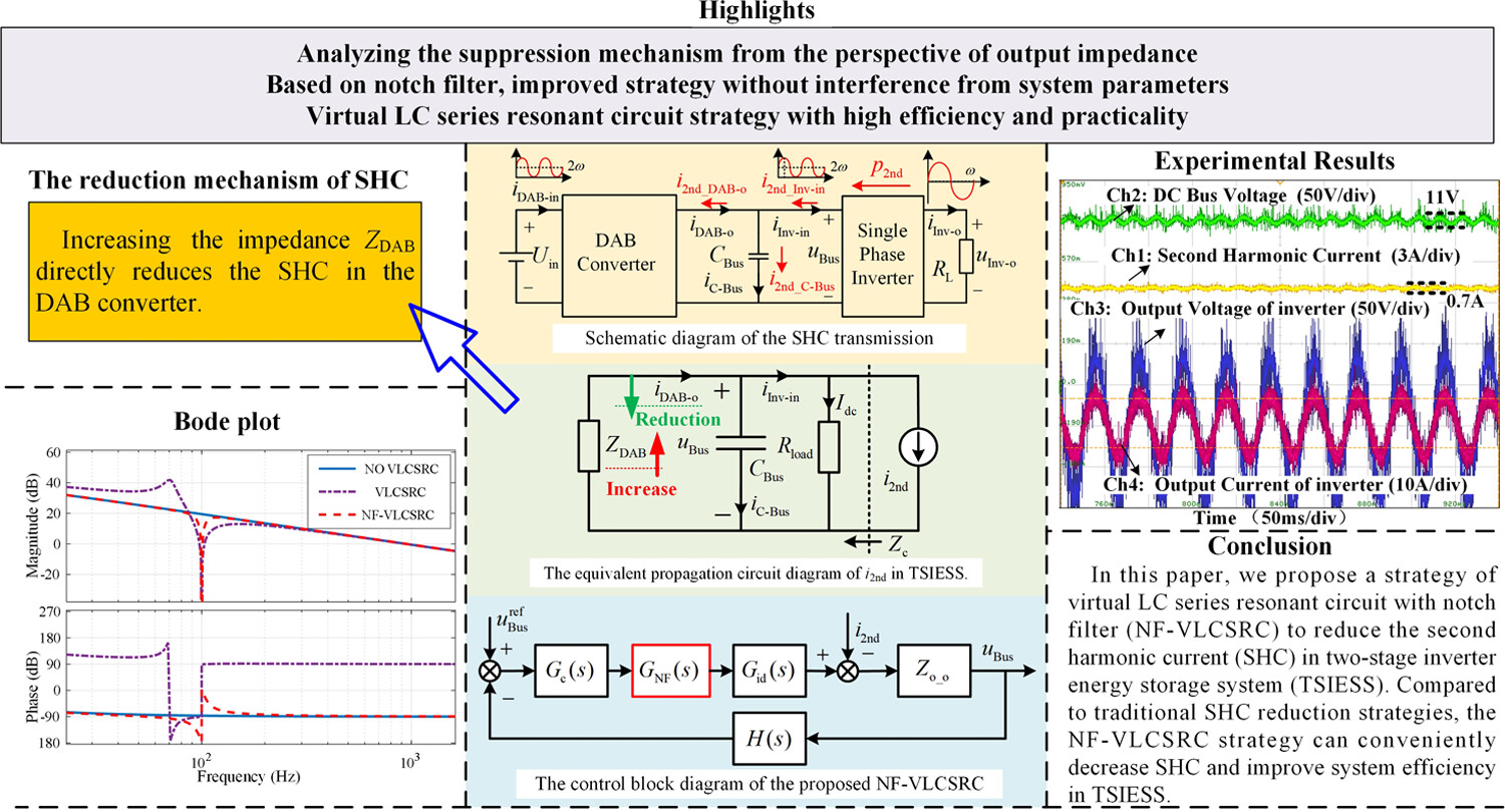
To reduce the SHC, this paper proposes a strategy of virtual LC series resonant circuit with notch filter (NF-VLCSRC). Compared with publicly available literature, this paper uses the principle of LC series resonant circuit to reduce SHC and analyzes the mechanism of reducing SHC from the perspective of output impedance.
A new class of active impedance source inverter with low voltage stress on semiconductors
- Pages: 5074-5106
- First Published: 21 March 2024
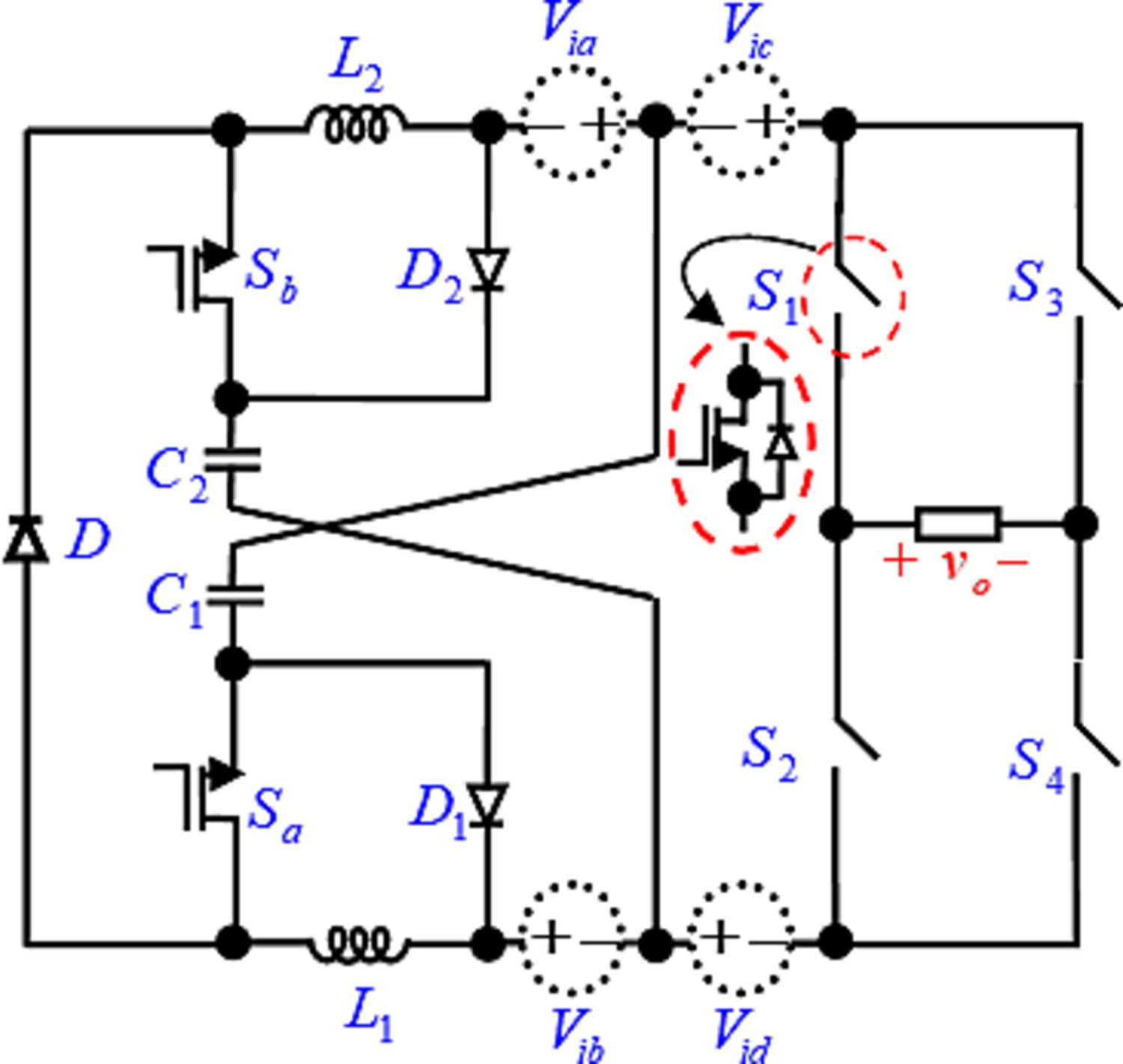
In this paper, a new group of active impedance source inverters, along with a suitable control method based on the pulse width modulation (PWM) technique, is presented. Using the proposed control method to produce the gate pulse of the switches, all operating modes of one of the proposed inverters, in two different operations (synchrony and asynchrony), to calculate boost factor and critical inductance in the boundary condition, are analyzed. The comparative analysis from different points of view, such as boost factor, total voltage blocked by diodes and switches, and voltage stresses on capacitors between the proposed topology and conventional structures to examine the advantages and disadvantages, is done.
A multi-objective optimization approach for modeling and analyzing the impact of drive parameters in SiC power converters
- Pages: 5107-5122
- First Published: 15 March 2024
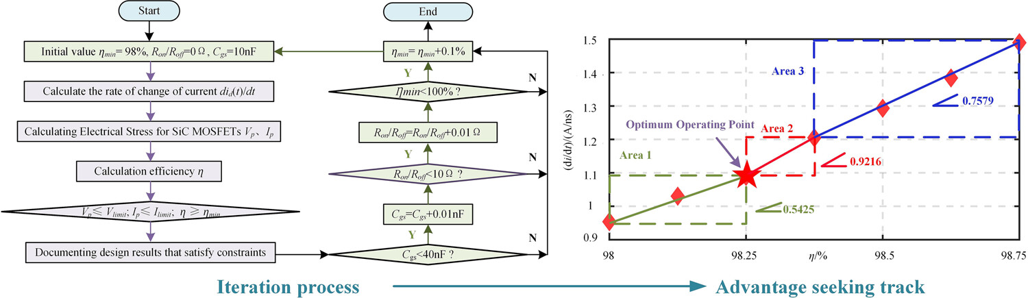
During iterations, as the efficiency constraint increases, the efficiency constraint of the previous iteration is the maximum efficiency that the converter can achieve when no results exist. Meanwhile, the current change rate and the corresponding driving parameters can be obtained. Based on the slope of the current change rate and the efficiency, the Pareto solution can be divided into three areas. Among them, Areas 2 and 3 have a more obvious efficiency improvement than Area 1, but Area 3 also brings a higher current change rate lift after passing through Area 2. Therefore, the intersection of Areas 1 and 2 is the best compromise point for efficiency and electrical stress.
A zero-input-current-ripple high-voltage-gain DC-DC converter with integrated Y-source network
- Pages: 5123-5143
- First Published: 15 March 2024
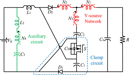
This paper proposes a zero-input-current-ripple (ZICR) high-voltage-gain dc-dc converter with an integrated Y-source network. It achieves zero input current ripple by introducing a parallel branch of an extra inductor, a coupled winding, and a capacitor at the input port. The voltage of the added inductor is opposite to that of the coupled winding. By adding the Y-source coupled inductor, the boost capability of the converter is improved. The unique boost circuit structure makes that one winding in the three-winding coupling inductance is step-down type (the turns ratio n2 < 1) while the other winding is step-up type (the turns ratio n1 > 1). In such a case, high voltage gain can be obtained under a lower turn ratio of the coupled inductor. The inherent passive clamping circuit clamps the spike voltage noises of the main switch to a low level and improves the efficiency. All the diodes have achieved ZCS (zero current switching) turn-off. By comparing with several new converters, the advantages of this converter are proved. Finally, a 200-W, 48- to 380-V, 50-kHz experimental prototype is built based on the theoretical research. At the rated power, the measured efficiencies with and without ZICR are 95.2% and 95.6%, respectively.
Commutation torque ripple suppression method for brushless DC motors with minimum phase shift angle
- Pages: 5144-5165
- First Published: 29 February 2024
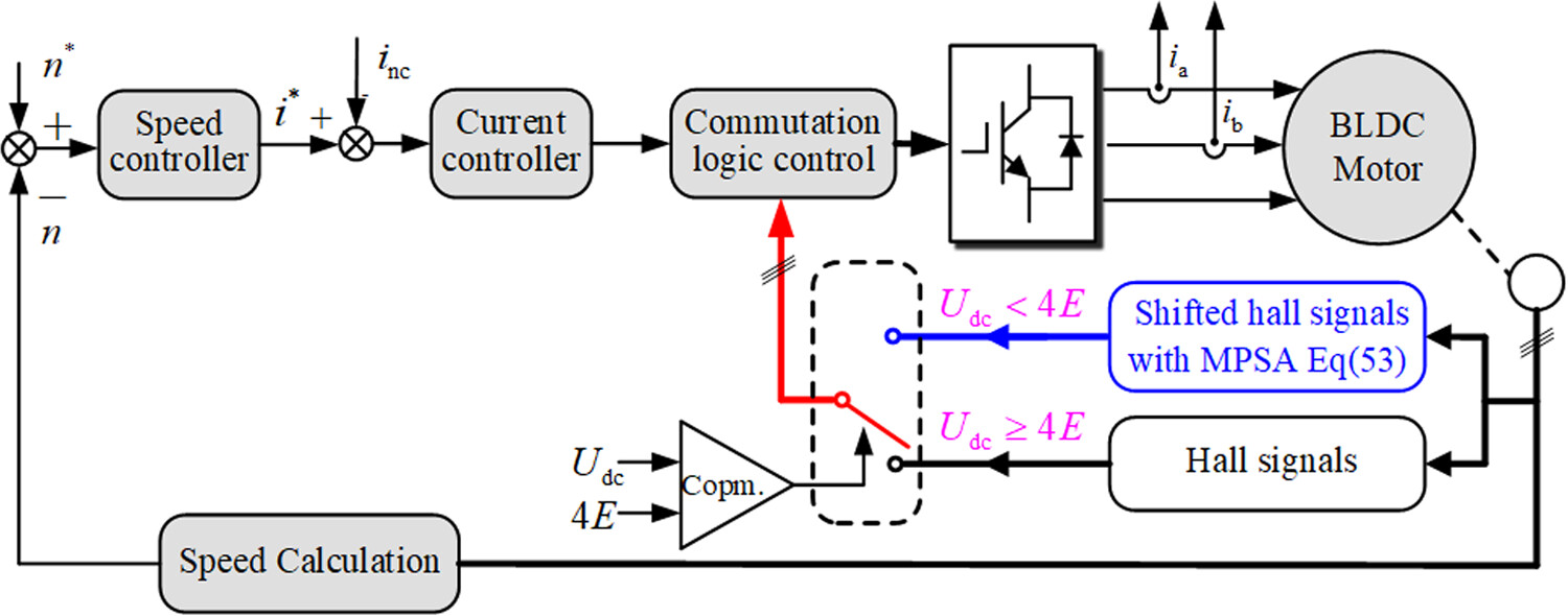
This paper presents a commutation torque ripple suppression method based on the minimum phase shift angle (MPSA) of hall signals. It is implemented through shifting hall signals by the MPSA and the MPSA is derived based on the unit duty cycle of the incoming and non-commutation phase. With the proposed method, the reliability is enhanced and no hardware is required, which reduces design cost and volume size. Finally, the proposed method is verified through simulation and experimental results.
Calculation and regulation of mutual inductance of wireless charging coils with metal shielding materials based on multiple intelligent optimization algorithms
- Pages: 5166-5183
- First Published: 28 February 2024
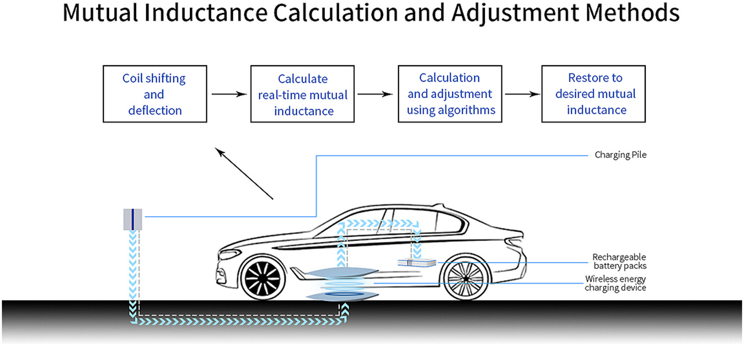
We derived the formula for calculating the mutual inductance value of a circular coil with a double-layer metal shielding material and designed a fast calculation and adjustment strategy for the mutual inductance value of the coil using an intelligent optimization algorithm.
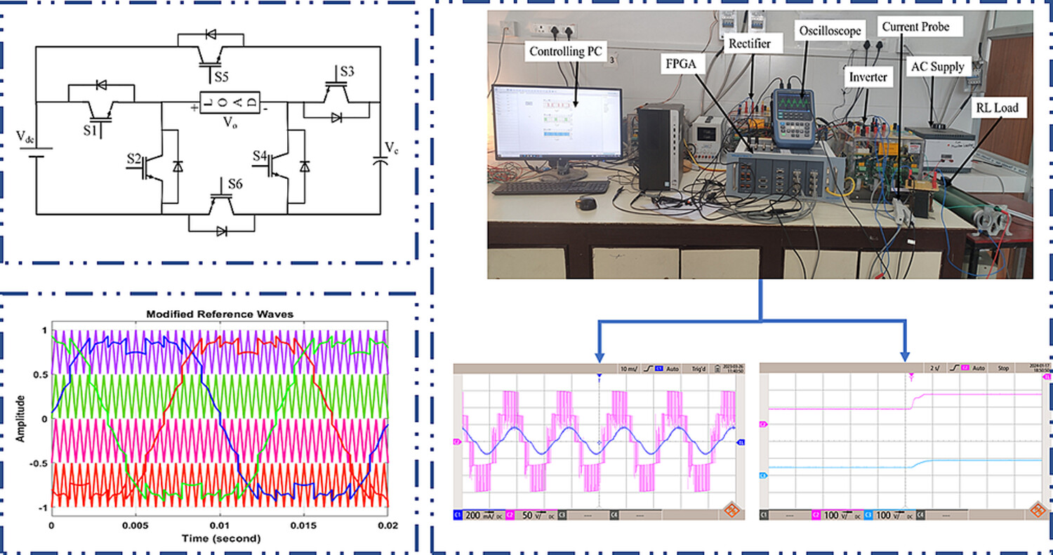
A novel UEBASC-qZSI-based BLDC motor drive with modified DTC for EV application
- Pages: 5184-5204
- First Published: 03 March 2024
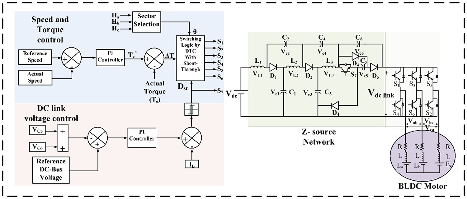
This research suggests to enhance the performance of electric vehicles (EVs) by integrating the proposed Ultra-Extended Boost Active Switch Controlled Quasi Z-source Inverter (UEBASC-qZSI) to power a BLDC motor. The implementation of a modified direct torque control method alongside UEBASC-qZSI aims to minimize torque distortion, resulting in improved EV efficiency and enhanced overall driving cycle safety. To verify the system's effectiveness, a Simulink model is developed in the MATLAB platform and is experimentally validated through a hardware prototype model.
Asymmetrical multi-level inverter by using space vector pulse width modulation technique for low and medium power applications
- Pages: 5205-5225
- First Published: 10 March 2024
This paper introduces a single-phase five-level inverter design using one DC source and a capacitor that possesses self-voltage balancing capability. The gate pulses are generated by using both SPWM and SVPWM techniques. Experimental setups and real-time implementation confirmed the viability of the proposed topology highlighting various applications.
Utilizing signal flow graph on multiple feedback amplifiers of NMC and DACFC with emphasis on design space exploration and conversion
- Pages: 5226-5251
- First Published: 18 March 2024
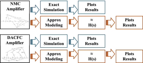
The article's approach to circuit and system simulation is illustrated in the graphical image. Circuit simulations of NMC and DACFC amplifiers are discussed using HSPICE. The approximate transfer functions (TFs) are calculated by mapping the amplifiers to the graph domain to compare the accuracy between circuit and system simulation results.
Three-phase common-ground-type photovoltaic inverter without shoot-through problem
- Pages: 5252-5262
- First Published: 20 March 2024
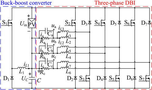
The three-phase common-ground-type transformerless dual-buck inverters (DBIs) are derived. By shorting the neutral point of the three-phase load and the negative terminal of the PV panel, the common mode leakage current (CMLC) is eliminated. The DBIs have no shoot-through problem, and there is no current flowing through the body diode of the SiC MOSFET.
Modeling, simulation, and experimental studies of a novel battery charger for fuel cell applications based on a new high step-up DC-DC converter
- Pages: 5263-5294
- First Published: 15 March 2024
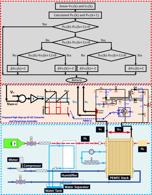
This work emphasizes the critical role of a well-designed high-efficiency DC-DC converter in the context of proton exchange membrane fuel cell (PEMFC) electric vehicle battery charging system. The proposed converter's innovative design, minimal componentry, efficiency, and validated performance through simulation, experimentation, and theory underscore its potential significance in enhancing PEMFC vehicle technology.
A novel 13-level switched-capacitor step-up inverter with reduced component count
- Pages: 5295-5317
- First Published: 05 March 2024
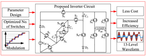
The proposed 13-level reduced multilevel inverter prioritizes optimized switch count for increased efficiency, utilizing Nearest Level Control (NLC) modulation for precise waveform control. This innovative design delivers cost-effectiveness without compromising performance, offering a compelling alternative to traditional multilevel inverters.
Harmonic suppression of active disturbance rejection control for virtual synchronous generators
- Pages: 5318-5337
- First Published: 04 March 2024
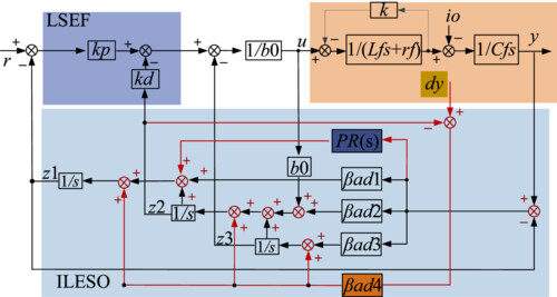
The implementation of a harmonic suppression strategy for VSG based on an enhanced linear extended state observer and PR-LADRC. The objective is to augment power quality by effectively mitigating harmonic disturbances in the system.
Stacked bidirectional DC-DC converter based on classical boost/buck converter for uninterruptible power supply applications
- Pages: 5338-5356
- First Published: 12 March 2024
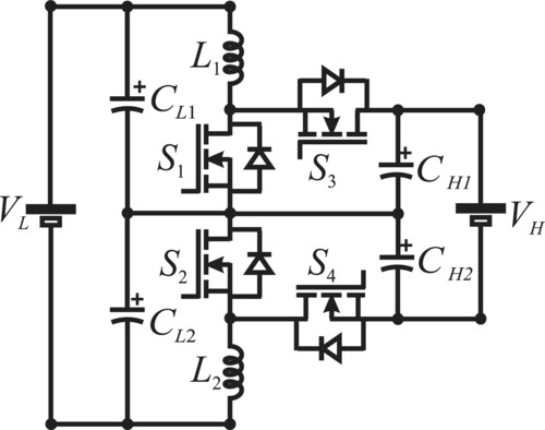
The paper presents an innovative stacked bidirectional nonisolated DC-DC converter designed for UPS applications. This advanced system boasts efficiency, simplicity, and a minimized component count. Model validation and comparative evaluations underscore its superior performance. A 1 kW prototype validates practical viability, achieving an impressive 96.38% efficiency in step-up and 95.7% in step-down modes.
Integrated modular equalization circuit for energy storage system
- Pages: 5357-5373
- First Published: 15 March 2024
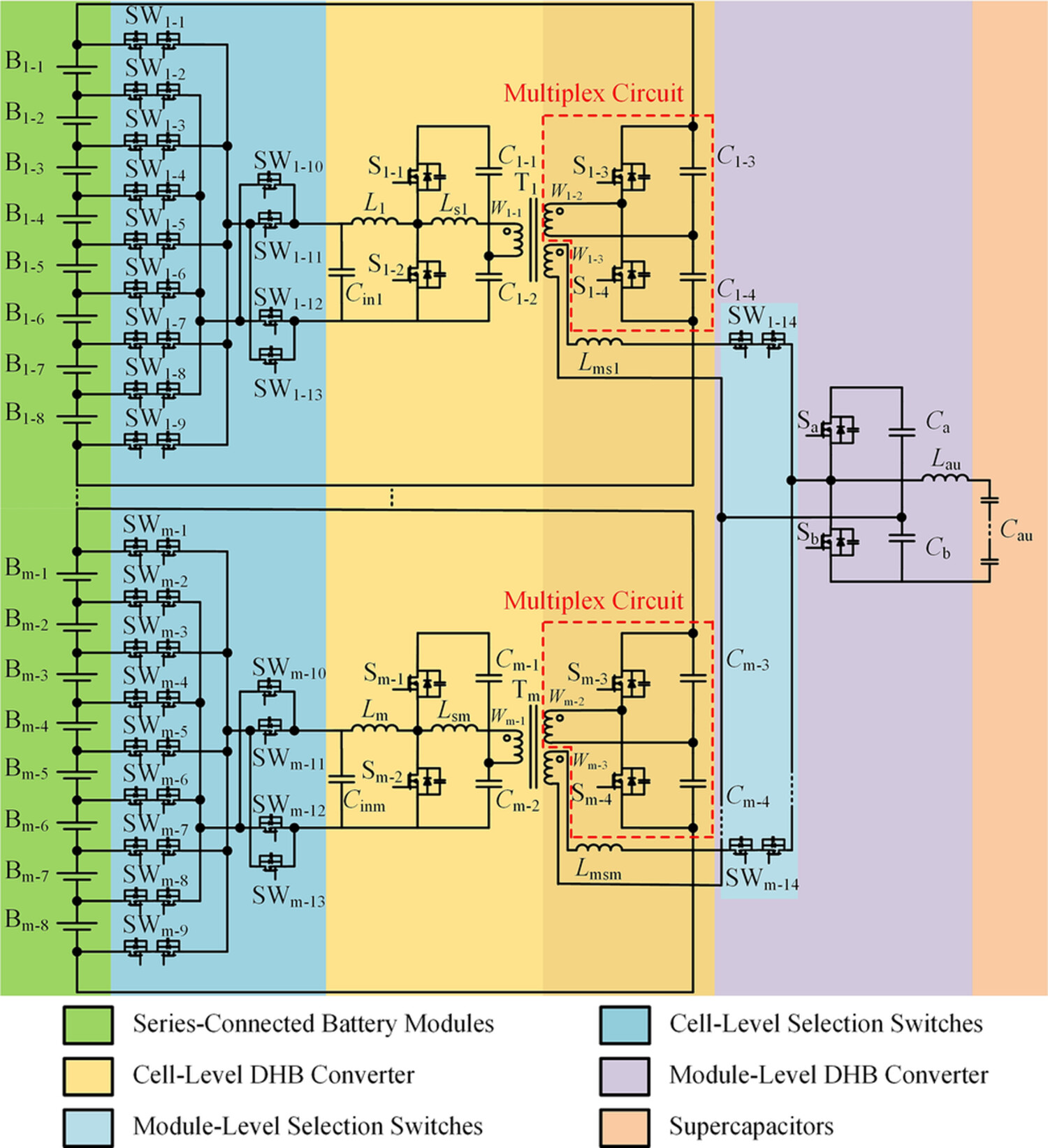
This paper proposes an integrated modular equalization circuit for energy storage systems. This integration is achieved by reusing the half-bridge circuit into the cell-level equalization circuit and the module-level equalization circuit, thereby simplifying the system and saving costs.
An ultra low-power double-node-upsets hardened latch design
- Pages: 5374-5389
- First Published: 24 March 2024
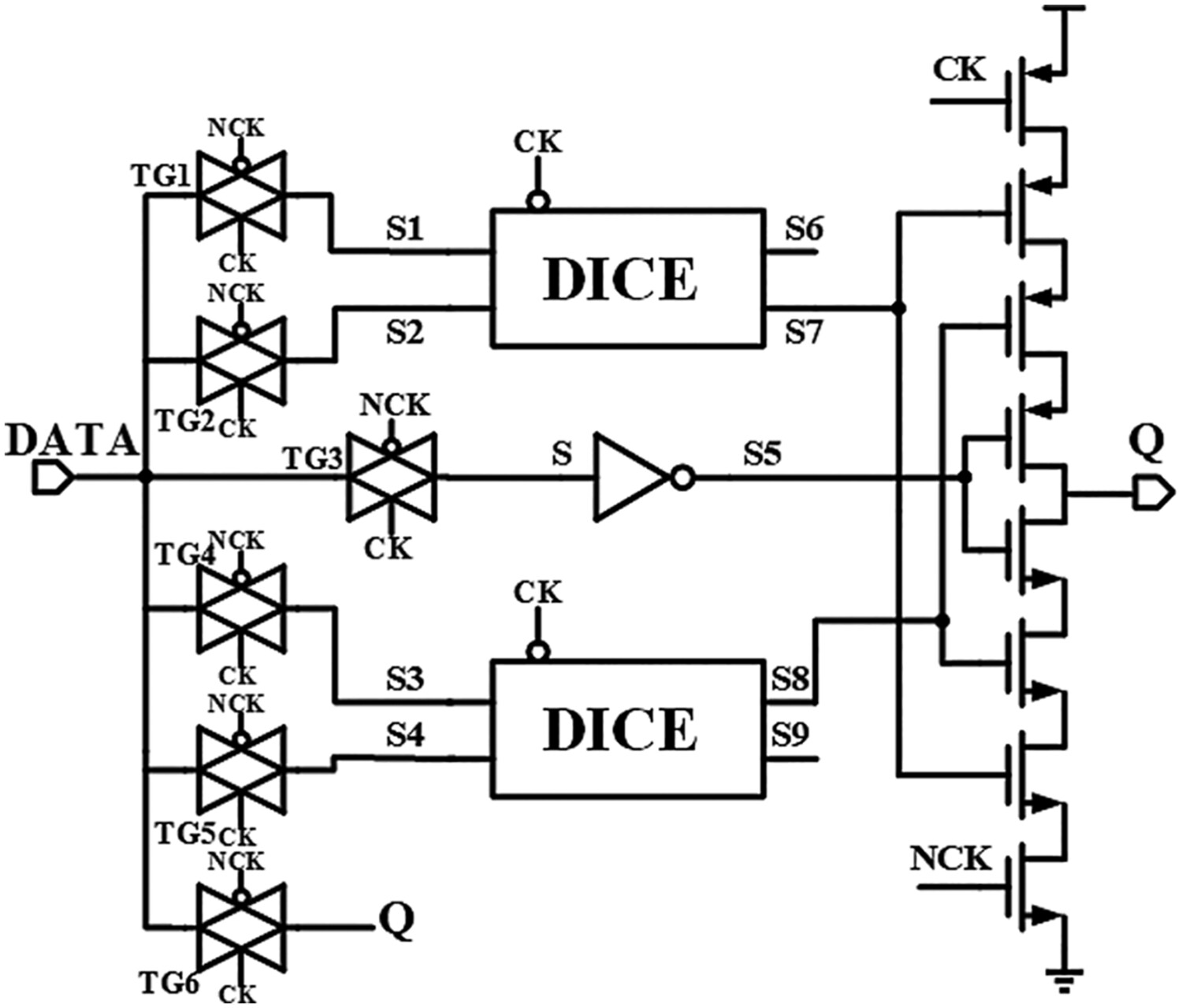
In order to reduce the influence of double-node upset (DNU) on latches in single-event effects (SEE) and solve the problem of high power of the other latches, a new radiation hardened by design (RHBD), namely low-power double-node-upsets hardened latch (LPDHL) based on dual-interlocked storage cell (DICE) is proposed.
Construction of logic circuit with modular molecular switching strategy based on DNA strand displacement
- Pages: 5390-5402
- First Published: 01 April 2024
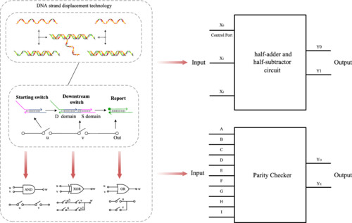
In this paper, we construct molecular switch circuits (MSCs) using DNA strand displacement. These circuits enable the realization of functions such as AND, OR, Fan-in, and Fan-out by cascading switches in series or parallel configurations. Additionally, we demonstrate the feasibility of these circuits by constructing a half-adder, half-subtractor, and a 9-bit parity checking circuit.
Design of unbalanced 9:2 ternary encoder and 2:9 ternary decoder circuits in resistive random access memory and carbon nanotube field effect transistor technology
- Pages: 5403-5426
- First Published: 21 March 2024
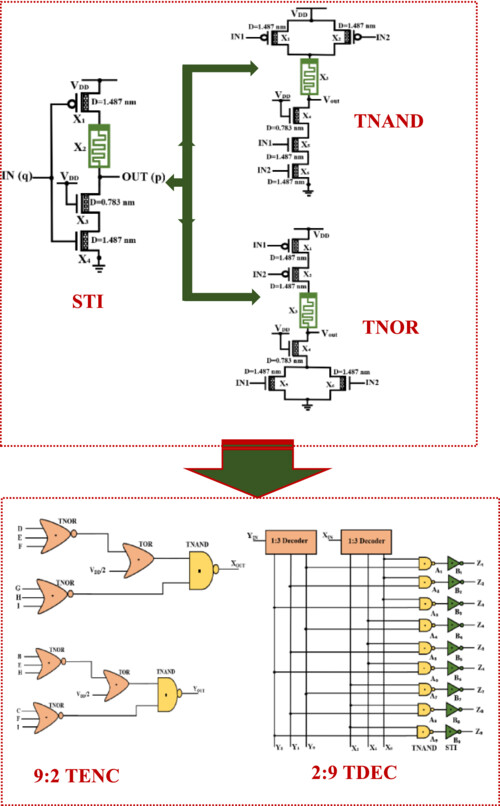
This paper presents designs of 9:2 unbalanced ternary encoder and 2:9 unbalanced ternary line address decoder based on novel designs of standard ternary inverter, ternary NAND, and ternary NOR logic gates using RRAM and CNTFET technology. Results indicate an improvement in power consumption, delay, power–delay product, and component count in comparison with the different existing counterparts. Moreover, a detailed analysis is carried out on the impact of PVT variations on the performance metrics of the proposed designs.
BRIEF REPORT
On the realization of an amplifier-tuned low/high frequency family of oscillators
- Pages: 5427-5435
- First Published: 01 April 2024
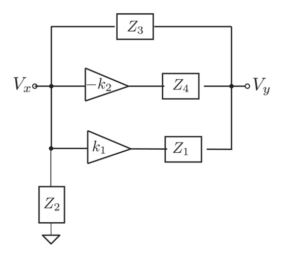
This graphical image describes an oscillator built around four impedances and two gain stages. The impedances can be separate R and C impedances or series and parallel RC combintaions. The gain stages can be opamp-based inverting and noninverting amplifiers or use any other active device. High- and low-frequency oscillators can be constructed based on this topology.
Sign up for email alerts
Tools
More from this journal:
This journal supports the Wiley Research Diversity, Equity & Inclusion statement
Read the statement