
Journal list menu

 Issue
Issuephysica status solidi (RRL) – Rapid Research Letters: Volume 8, Issue 5
373-450May 2014
Export Citations
Download PDFs
Cover Picture
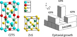
Cover Picture: Radio frequency magnetron sputtered epitaxial Cu2ZnSnS4 thin film on ZnS(100) (Phys. Status Solidi RRL 5/2014)
- First Published: 15 May 2014
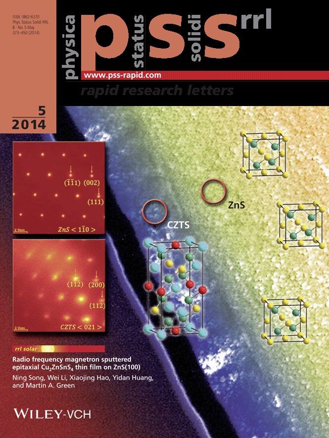
Cu2ZnSnS4(CZTS) is regarded as one of the most promising absorber materials for solar cells due to its earth-abundant composition, band gap energy of around 1.5 eV and the large absorption coefficient of over 104 cm–1. Environment-friendly and cost-effective CZTS thin-film solar cells are expected to be alternatives for commercialised Cu(InGa)Se2 and CdTe solar cells. However, the highest efficiency of CZTS so far is considerably less than that of Cu(InGa)Se2 of CdTe solar cells. To fully explore its potential, epitaxial growth of CZTS on ZnS(100) substrate was achieved by radio frequency magnetron sputtering for better understanding of the fundamental properties of the CZTS absorber (see the Letter by Ning Song et al. on pp. 404–407). The front cover image depicts a dark field scanning transmission electron microscopy image of the epitaxial CZTS film on ZnS(100), with insets on selective area electron diffraction patterns of the circled areas in the ZnS substrate and CZTS layer, respectively.
Back Cover
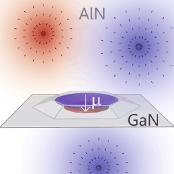
Back Cover: GaN nanowires for piezoelectric generators (Phys. Status Solidi RRL 5/2014)
- First Published: 15 May 2014
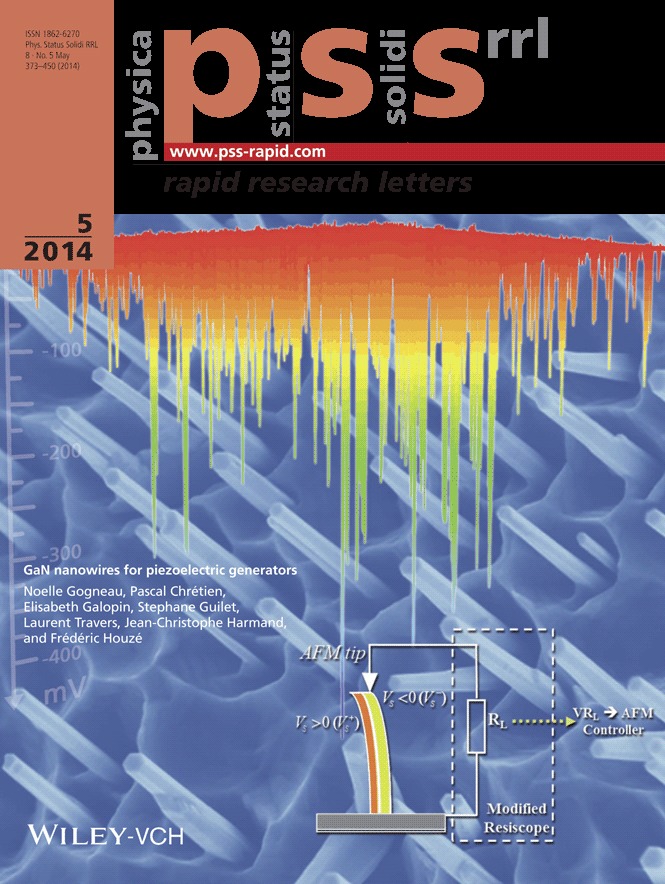
The semiconductor nanowires (NWs) presenting piezoelectric properties have recently emerged as excellent candidates to fabricate novel and efficient piezoelectric generators through the harvesting of mechanical deformations and vibrations energies. In particular, gallium nitride (GaN) NWs are characterized by both higher piezoelectric response and output voltages with respect to other piezoelectric material NWs. In their Letter on pp. 414–419, Noelle Gogneau et al. investigate the mechanical–electrical conversion of GaN NWs. An average output voltage of about –74 mV for a large NW ensemble and a maximum output voltage reaching –443 mV (±2%) per NW are demonstrated. This latter output voltage is the highest value reported so far for GaN NWs. Based on these measured output signals, an average and a maximum power density generated by one layer of GaN NWs of the order of 5.9 mW/cm2 and 130 mW/cm2, respectively, have been estimated. This result evidences the strong potentiality of GaN NWs to develop ultra-compact and integrable renewable energy source for sustainable, independent and maintenance-free operation of microdevices.
Issue Information
Contents
Contents: Phys. Status Solidi RRL 5/2014
- Pages: 373-378
- First Published: 15 May 2014
NEW IN pss
Recent and forthcoming publications in pss: Phys. Status Solidi RRL 5/2014
- Pages: 379-380
- First Published: 15 May 2014
rrl solar
Silicon solar cells
The BOSCO solar cell – a both sides collecting and contacted structure
- Pages: 381-384
- First Published: 28 April 2014
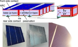
First results of the novel BOSCO (“BO th Sides CO llecting and CO ntacted”) solar cell structure on multicrystalline silicon are reported. A significant gain in monofacial efficiency of +0.7%abs compared to the industry standard of aluminium back surface field (Al-BSF) cells has been achieved. Due to double-sided current collection, the BOSCO cell is a promising candidate to enable bifacial applications for material of lower diffusion lengths, in contrast to most published structures requiring high diffusion lengths.
Localization and characterization of annealing-induced shunts in Ni-plated monocrystalline silicon solar cells
- Pages: 385-389
- First Published: 12 February 2014
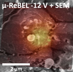
The adhesion and contact resistivity of plated solar cell front contacts on a nickel seed layer can be improved by thermal silicidation of the Ni–Si interface. Formation of deep local nickel sicilide structures harms the cell performance. In the presented Letter, critical silicide structures were localized with a precision of 1 μm in top view. Subsequent cross-section studies reveal micro-defects.
Organic photovoltaic cells
UV/ozone-treated WS2 hole-extraction layer in organic photovoltaic cells
- Pages: 390-394
- First Published: 02 May 2014
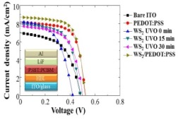
The power conversion efficiency (PCE) values of devices with and without untreated WS2 are both 1.84%. After performing a UV-ozone (UVO) treatment on the WS2, the PCE increases to 2.4%. Upon inserting poly(3,4-ethylenedioxythiophene):poly(styrene sulfonate) (PEDOT:PSS) between the WS2 and the active layer, the PCE value increases to 3.07%, which is superior to that of the device employing only PEDOT:PSS (2.87%).
Surface passivation
Silicone oxidation for a-Si:H passivation of wafers bonded to glass
- Pages: 395-398
- First Published: 25 March 2014
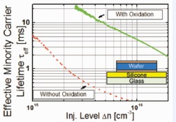
A method to passivate the surface of a wafer/silicone/glass stack to state-of-the-art values (SRV < 4 cm/s) is presented. The method is based on an O2-plasma and an HF/TMAH/HF cleaning sequence that increase the silicone cross-linking and its resilience to process-induced degradation. The method is proven to work for three different silicone-based photovoltaic (PV) encapsulants and is believed to significantly broad the adhesive choice for module-level processing of wafer-based silicon solar cells.
Hybrid structures
Hybrid silver nanoparticle and transparent conductive oxide structure for silicon solar cell applications
- Pages: 399-403
- First Published: 17 February 2014
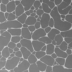
A hybrid structure, consisting of a transparent conductive oxide layer and a silver nanoparticle mesh, is demonstrated to have high electrical conductance (<5 Ω/square sheet resistance) and high visible transparency (∼86%). This structure enables a separate optimization of the electrical and optical requirements, which provides benefits for applications in solar cells and other devices.
Kesterite thin films
Radio frequency magnetron sputtered epitaxial Cu2ZnSnS4 thin film on ZnS(100)
- Pages: 404-407
- First Published: 06 May 2014
Environment-friendly and cost-effective Cu2ZnSnS4 (CZTS) thin film solar cells are expected to be alternatives for commercialized Cu(InGa)Se2 (CIGS) and CdTe solar cells. In this Letter, epitaxial growth of CZTS on ZnS (100) substrate was achieved by radio frequency magnetron sputtering from a single CZTS target for investigation of the fundamental properties of the CZTS absorber itself.
Rapid Research Letters
Nitride quantum dots
Spectral diffusion in nitride quantum dots: Emission energy dependent linewidths broadening via giant built-in dipole moments
- Pages: 408-413
- First Published: 15 April 2014
Huge excitonic dipole moments inherent to wurtzite GaN/AlN quantum dots cause their particular vulnerability to emission line widths broadening in contrast to less-polar systems (e.g. arsenides). Defect-induced charges in the vicinity of these nitride quantum dots interact with the confined excitons, continuously affecting their emission energy, as approved by the presented emission line widths statistics for hundreds of individual emitters.
GaN nanowires
GaN nanowires for piezoelectric generators
- Pages: 414-419
- First Published: 15 April 2014
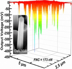
The mechanical–electrical conversion of GaN nanowires (NWs) is investigated. An average output voltage of about –74 mV for a large NW ensemble and a maximum output voltage reaching –443 mV ± 2% per NW are demonstrated. This latter output voltage is the highest value reported so far for GaN NWs and offers promising prospects for high-efficiency piezogenerators.
MAX phases
Synthesis and characterization of arc deposited magnetic (Cr,Mn)2AlC MAX phase films
- Pages: 420-423
- First Published: 07 April 2014
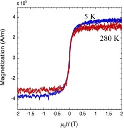
Epitaxial (Cr1–xMnx)2AlC (x = 0.2) thin films were synthesized by cathodic arc deposition. Vibrating sample magnetometry measurements reveal (Cr,Mn)2AlC as a new member in the recently discovered group of magnetic MAX phases. Magnetic transition temperature significantly higher than room temperature and magnetic moment >0.16 μB/M-atom are concluded.
Blue light emitting diodes
Blue light emitting diode exceeding 100% quantum efficiency
- Pages: 424-426
- First Published: 04 February 2014
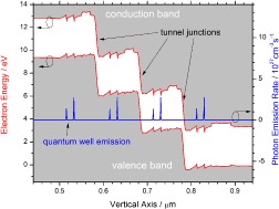
The Letter demonstrates a new approach to enhancing the quantum efficiency of GaN-based light emitting diodes by insertion of multiple tunnel junctions into the active region which allow for the repeated use of electrons and holes for photon generation.
New sensing methods
Refractive index sensing by using Fano resonance enhanced two-photon luminescence
- Pages: 427-430
- First Published: 28 March 2014
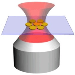
Fano resonance assisted two-photon luminescence in the plasmonic heptamer can be used to realize high performance refractive index sensing. The sensitivity of this method is about one order of magnitude better than the conventional refractive index sensing strategy utilizing Fano resonance while the size of the sensing probe can be further reduced at the same time.
Y2O3/TiOx RRAM
Improved high-temperature switching characteristics of Y2O3/TiOx resistive memory through carrier depletion effect
- Pages: 431-435
- First Published: 22 April 2014
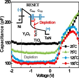
Due to the barrier-height lowering at high temperature, the apparent degradation on sneak current and current distribution are major challenges, especially for the scaled one-diode–one-resistor (1D1R) resistive random access memory (RRAM) crossbar arrays. Therefore, the excellent high-temperature switching properties are important for production. In this study, the lower high-temperature sneak current and tighter high-temperature current distribution can be reached by Y2O3/TiOx RRAM structure, which has the potential for future application.
Graphene quantum dots
Quantum confinement in graphene quantum dots
- Pages: 436-440
- First Published: 31 March 2014
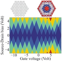
In this Letter, the authors studied the quantum confinement in charged graphene quantum dots (GQDs), which is found to be clearly edge and shape dependent. It is revealed that the charged GQD is characterized by highly non-uniform excess charge distribution, irregular Coulomb diamonds, random energy spectrum shift and level statistics suggesting quantum chaos.
Graphene films
Layer-by-layer AuCl3 doping of stacked graphene films
- Pages: 441-444
- First Published: 20 March 2014
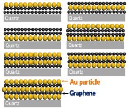
The authors investigated the effect of layer-by-layer AuCl3 doping on the electrical and optical properties of stacked graphene films. Graphene was chemically doped by AuCl3 solution. Different configurations are characterized by using four-point probe measurements, optical transmittance measurements, scanning electron microscopy, and micro-Raman spectroscopy. Better performances considering both sheet resistance and optical transmittance are observed from the configurations with the top-layer doped.
Zinc-blende axial nanowires
Plastic relaxation of mixed dislocation in axial nanowire heterostructures using Peach–Koehler approach
- Pages: 445-448
- First Published: 10 April 2014
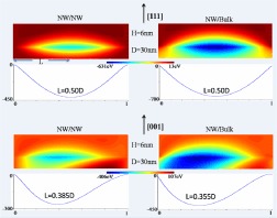
Avoiding misfit dislocation generation in nanowire (NW) heterostructure with lattice mismatch is a crucial topic for high-quality heteroepitaxy. In this Letter, the plastic relaxation introduced by typical 60° mixed dislocation in zinc-blende axial NW heterostructures are evaluated by numerical Peach–Koehler approach. The equilibrium position and critical diameter are theoretically predicted for cylindrical NW epilayers grown on both NW and bulk substrates.
Information for authors
Information for authors: Phys. Status Solidi RRL 5/2014
- Pages: 449-450
- First Published: 15 May 2014
Sign up for email alerts
Tools
![]()
In 2022, the youngest family member physica status solidi (RRL) – Rapid Research Letters is turning 15 years. To celebrate this milestone, we present a new virtual collection with invited articles.
![]()
As we celebrate the 60th anniversary year of the physica status solidi family, click here to access our continuously updated collection of invited articles written by authors and partners of the pss journals.