

Journal list menu

 Issue
IssueInternational Journal of Circuit Theory and Applications: Volume 50, Issue 6
1817-2287June 2022
Export Citations
Download PDFs
ISSUE INFORMATION
ORIGINAL PAPERS
A PVT power immune compact 65 nm CMOS CSP design with a leakage current compensation feedback for CdZnTe/CdTe sensors dedicated to PET applications
- Pages: 1817-1833
- First Published: 04 March 2022
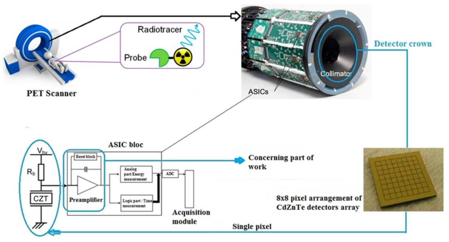
In most readout integrated circuits (ROIC) chips of pixelated Cadmium-Telluride (CdTe)/Cadmium-Zinc-Telluride (CdZnTe) sensors for nuclear magnetic resonance imaging (MRI) and positron emission tomography (PET) applications, the quality of the images is improved due to reducing nonlinearity errors in the front-end electronics (FEEs). This leads to increasing the detection efficiency by integrating monolithically the sensor chip and the FEE within a complementary metal-oxide semiconductor (CMOS) device. The key ROIC element, namely, preamplifier, is needed to be implemented with the highest possible accuracy and should guarantee low noise, low power, and high linearity along with assuring higher conversion gain and less chip area.
A 23- to 28-GHz 5-bit switch-type phase shifter with 1-bit calibration based on optimized ABCD matrix design methods for 5G MIMO system in 0.15-μm GaAs
- Pages: 1834-1854
- First Published: 24 February 2022
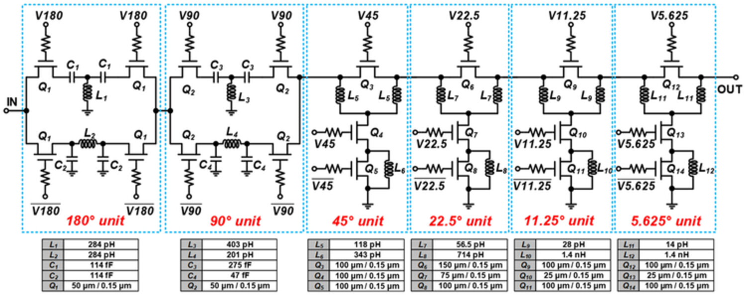
This paper reports a 23-28 GHz 5-bit switch-type phase shifter with 1-bit calibration in 0.15-μm GaAs process. A new design method based on the optimized ABCD matrix and impedance matching techniques between a chip and a printed circuit board is developed to obtain better radio-frequency signal transmission. The proposed phase shifter features a good phase performance with a measured root mean square phase error of less than 10° across 23-28 GHz.
A 60-GHz low-noise amplifier with +7.258-dBm third-order input intercept point using current reuse feedforward distortion cancellation for 5G emerging communication
- Pages: 1855-1875
- First Published: 06 March 2022
A 60-GHz mmWave LNA is proposed for high-throughput, low-power, and low-noise receivers operating in the unlicensed band of 57–66 GHz. The current reuse feedforward distortion cancellation technique for linearity enhancement is employed along with the low-noise CG input stage which reduces the circuit noise than the ever used 60-GHz LNA architectures such as CS-CS and cascode topology.
130-nm BiCMOS design of low-pass negative group delay integrated RL-circuit
- Pages: 1876-1889
- First Published: 07 March 2022
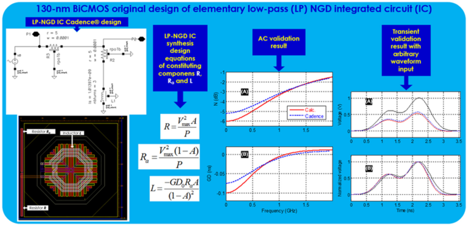
This paper presents an innovative 130-nm BiCMOS design of LP-NGD integrated circuit (IC). The analysis and synthesis method of RL-network based IC is developed. The effectiveness of the method is validated by CADENCE VIRTUOSO simulation in both frequency and time domain.
A new harmonic tuned class E power amplifier based on waveform analysis
- Pages: 1890-1906
- First Published: 08 March 2022
A waveform theory for harmonic tuned class E power amplifier based on waveform analysis is proposed. This paper replaces the output impedance in the traditional Class E PA design with the output impedance obtained from the waveform analysis, which makes the design of the matching network more convenient and ensures that the output current waveform and voltage waveform of the designed new HT class E PA are very close to those of the ideal Class E power amplifier.
Synthesis of wideband bulk acoustic wave coupled resonator filter combined with lumped components
- Pages: 1907-1921
- First Published: 13 March 2022
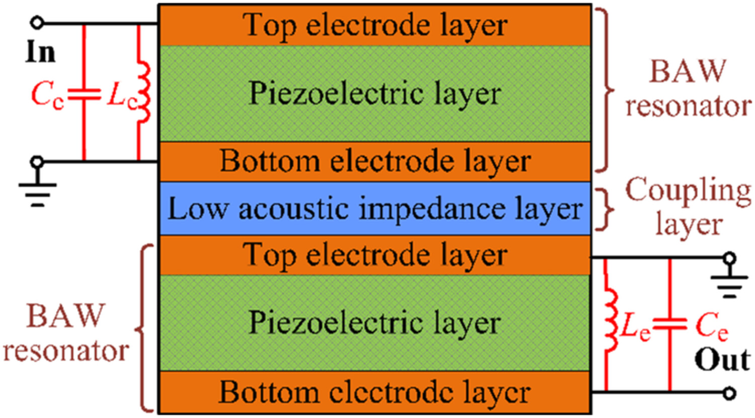
- A wideband BAW CRF is proposed by introducing external inductors and capacitors, which exhibits a maximum 37.4% FBW with 9.4-dB return loss.
- A synthesis method for wideband CRF design is also developed. Though the synthesis method, exact CRF dimensions can be solved through a set of equations without any further parameters tuning.
- A n77 band filter is designed and simulated to verify the proposed CRF and synthesis method.
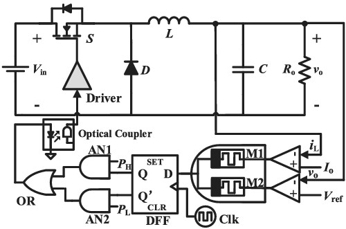
Analysis of single input dual output buck converter with reduced cross regulation using decoupled sliding mode control strategy
- Pages: 1922-1945
- First Published: 03 February 2022
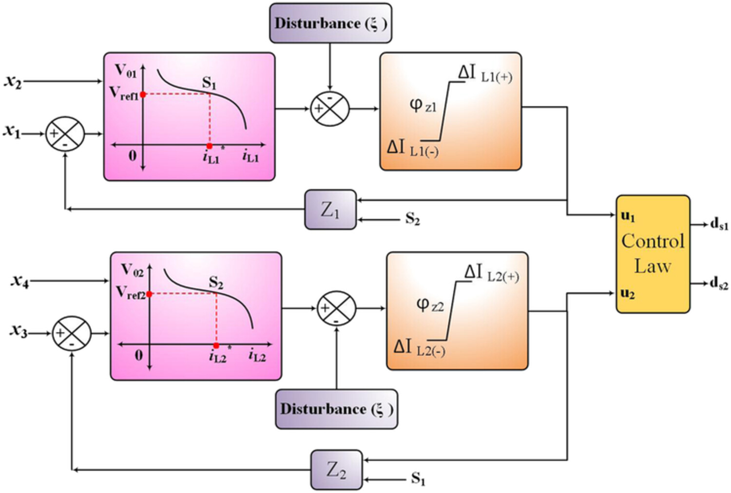
This article analyzes the design of decoupled sliding mode controller for mitigating the cross regulation in SIDO buck converters.
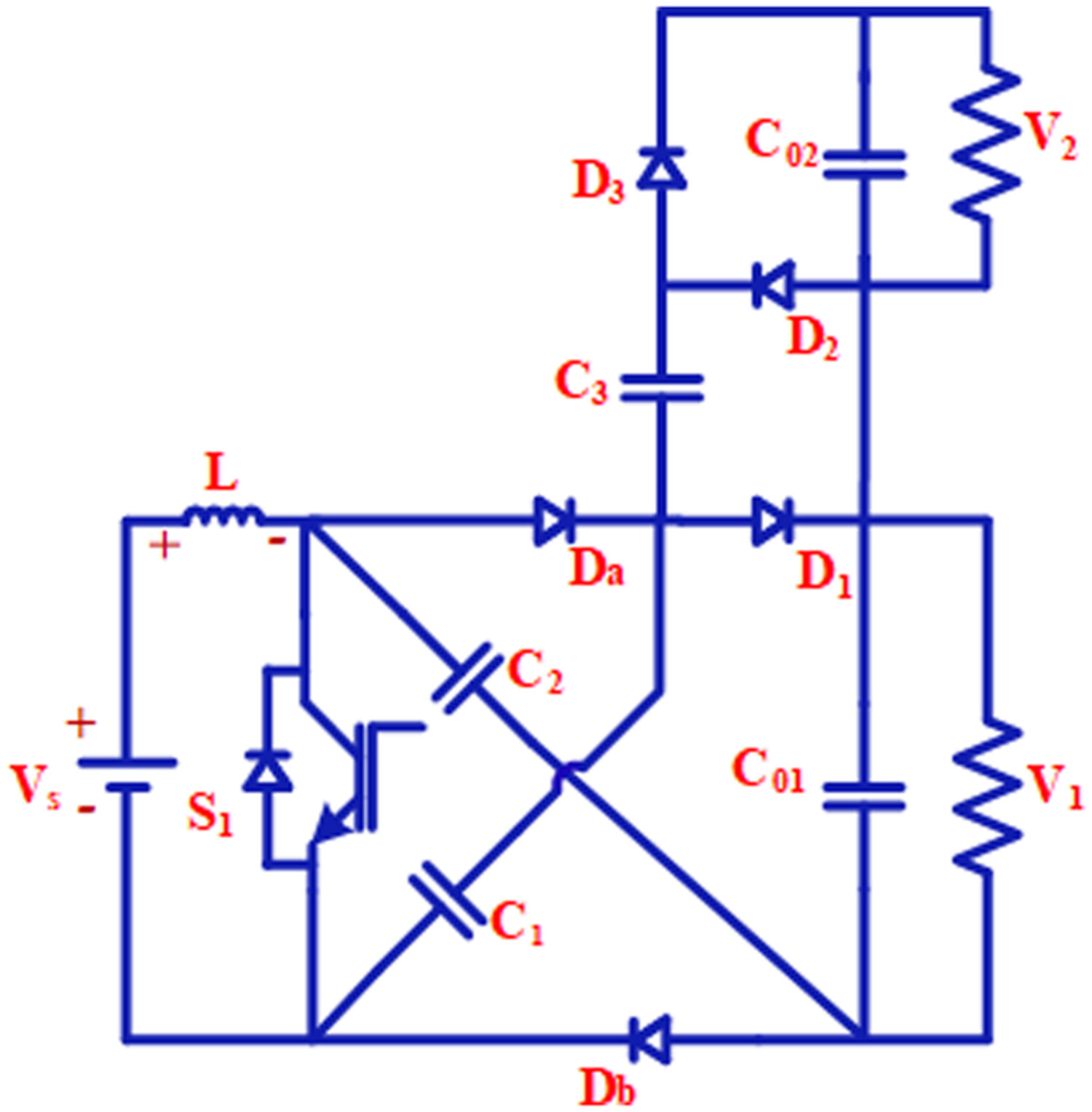
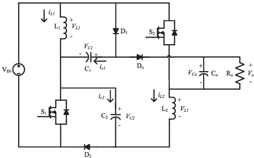
Non-isolated high step-up DC/DC converter for low-voltage distributed power systems based on the quadratic boost converter
- Pages: 1946-1964
- First Published: 08 February 2022
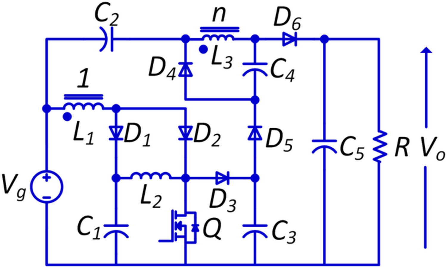
This paper proposes a new non-isolated step-up DC/DC converter that can be used in low-voltage distributed power systems and many other applications requiring step-up DC/DC conversion. The topology requires only one power switch located on the converter's low voltage (LV) side. Compared with the recently proposed topologies, the topology provides better conversion gain and efficiency.
Sensorless voltage balancing method for modular multilevel converter
- Pages: 1965-1997
- First Published: 09 February 2022
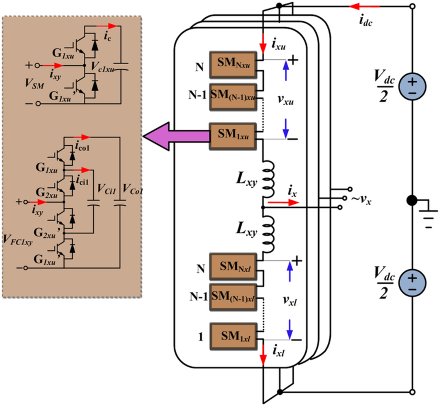
This paper proposes a sensorless capacitor voltage balancing method with single carrier PWM for modular multilevel converter. It ensures uniform power distribution and achieves the voltage balance control without voltage and current sensors. The proposed method is analyzed mathematically and verified with 2L-half-bridge submodules and 3L-flying capacitor submodules. The simulation and experimental results validate the method.
High-gain single-switch single-input dual-output DC-DC converter with reduced switching stress
- Pages: 1998-2015
- First Published: 11 February 2022
This paper presents a novel of a single-switch single-input dual-output DC-DC converter with a high-gain ratio. It attains the two boosted outputs with a high-gain conversion ratio using a single switch by incorporating the switched-capacitor technique. In addition, the bulkiness of the converter was reduced by utilizing only one inductor and switch. Moreover, it improves efficiency by reduced switching stress and cross-regulation at output ends.
An any-unit-to-any-unit method for hybrid-structured voltage equalizer in series-connected battery/super-capacitor strings
- Pages: 2016-2034
- First Published: 14 February 2022
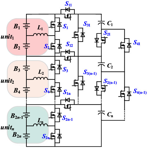
A hybrid-structured voltage equalizer (HSVE) is developed for battery strings to achieve high-speed any-unit-to-any-unit (AU2AU) equalization, in which each unit can also achieve internal balance in any arbitrary imbalance status. The proposed equalizer does not need any cell monitoring circuits. Hardware experiments on super-capacitors and Li-ion batteries are conducted in this study, which prove the feasibility of the proposed voltage equalizer.
Fully integrated switched-inductor switched-capacitor dual-path DC–DC converter
- Pages: 2035-2054
- First Published: 14 February 2022
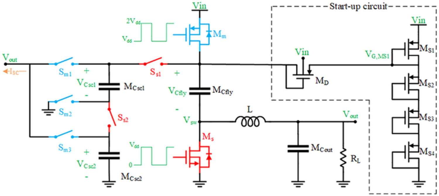
In this work, a method is presented to implement a fully integrated dc–dc converter. Input dc voltage higher than the maximum permissible voltage of the used technology is down-converted with high efficiency. This is because of using an optimized on-chip inductor and providing two parallel switched-capacitor and switched-inductor paths to supply the output power. This feature reduces the current flowing through the output series inductor and causes significant improvement of the inverter efficiency.
A non-isolated high voltage gain DC–DC converter based hybrid switched LC network for renewable energy applications
- Pages: 2055-2074
- First Published: 21 February 2022
A new high voltage gain DC–DC converter for renewable energy applications without the need for a galvanic isolation. The converter combines the active switched–inductor network and the switched-capacitor network to boost the voltage gain ratio without a high duty ratio.
Evaluation of a grid-connected reduced-component boost multilevel inverter (BMLI) topology
- Pages: 2075-2107
- First Published: 24 February 2022
In this paper, a reduced-component switched-capacitor boost multilevel inverter (SC-BMLI) topology is proposed for off-grid and on-grid applications. To generate a nine-level stepped-up voltage across the load, the SC-BMLI needs only eight power switches and two capacitors. The proposed inverter has low cost factor, voltage across capacitors is balanced, and it mitigates an inrush current due to switching of capacitor by employing a charging inductor. In the last, results are obtained by simulation, real-time study, and hardware implementation for the proposed nine-level boost multilevel inverter (BMLI).
Collaborative state estimation of lithium-ion battery based on multi-time scale low-pass filter forgetting factor recursive least squares - double extended Kalman filtering algorithm
- Pages: 2108-2127
- First Published: 25 February 2022
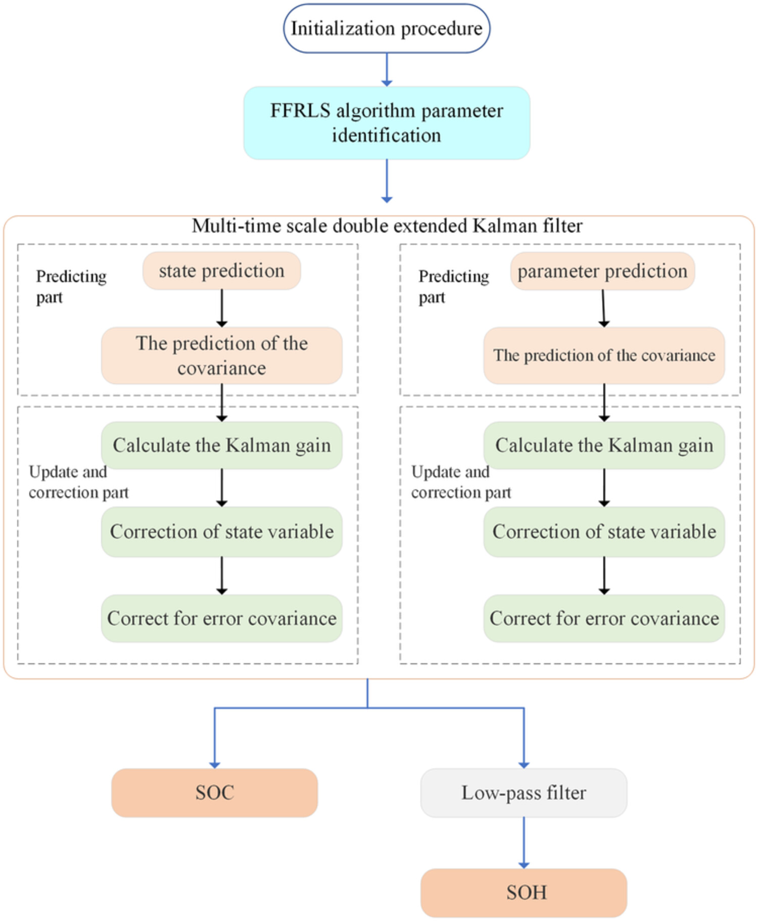
This thesis adopts the second-order RC equivalent circuit model and the forgetting factor recursive least squares - double extended Kalman filtering (FFRLS-DEKF) algorithm with multi-time scales and low-pass filter. Forgetting factor recursive least squares is applied to conduct online parameter identification, and the traditional DEKF algorithm is optimized to evaluate the state of charge and model parameters in the micro-scale and macro-scale. Low-pass filter is added to optimize the fluctuation problem of the estimated value of the model parameters.
A novel voltage boosting switched-capacitor 19-level inverter with reduced component count
- Pages: 2128-2149
- First Published: 15 February 2022
A non-isolated switched inductor-capacitor cell based multiple high voltage gain DC-DC boost converter
- Pages: 2150-2174
- First Published: 03 February 2022
Hybrid soft switching DC–DC boost converter
- Pages: 2175-2189
- First Published: 08 March 2022
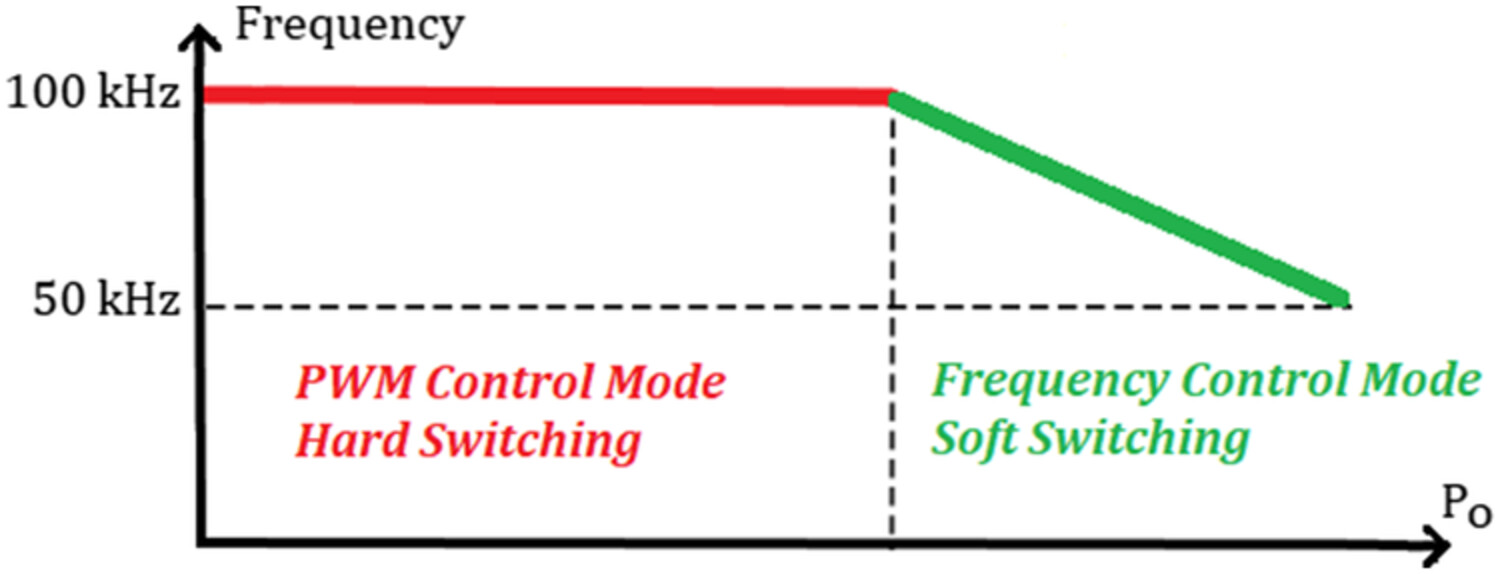
The hybrid concept is as follows: The proposed converter combines PWM and frequency control methods to increase efficiency and provide a simple active snubber cell structure.
Memristor-based logic gate and its application in pulse train controlled Buck converter
- Pages: 2190-2209
- First Published: 04 March 2022
Flux-controlled binary memristor (MR) emulator based logical gates are constructed and applied to pulse train (PT) controlled Buck converters to improve output voltage response performance. To suppress low-frequency voltage oscillation of PT controlled Buck converters in continuous conduction mode (CCM), inductor current based pulse train (IC-PT) control method using the MR-based logic gates is newly proposed for achieving fast transient response and minimized low-frequency voltage oscillation in CCM mode.
ORIGINAL ARTICLES
Comb decimator design based on symmetric polynomials with roots on the unit circle: Two-stage multiplierless design and improved magnitude characteristic
- Pages: 2210-2227
- First Published: 21 February 2022
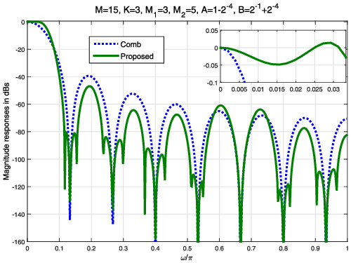
This paper presents a theoretical background for design of comb decimator based on theorem of symmetric polynomials with roots on the unit circle. A simple multiplierless filter, called zero-separation (ZS) filter, which separates doubled comb zeros, is derived and inserted in the second stage of a two-stage structure. The passband droop of the overall structure is compensated by the compensator which works at low rate and is designed using particle swarm optimization (PSO).
ORIGINAL PAPERS
Structure-induced low-sensitivity design of sampled data and digital ladder filters using delta discrete-time operator
- Pages: 2228-2251
- First Published: 18 February 2022
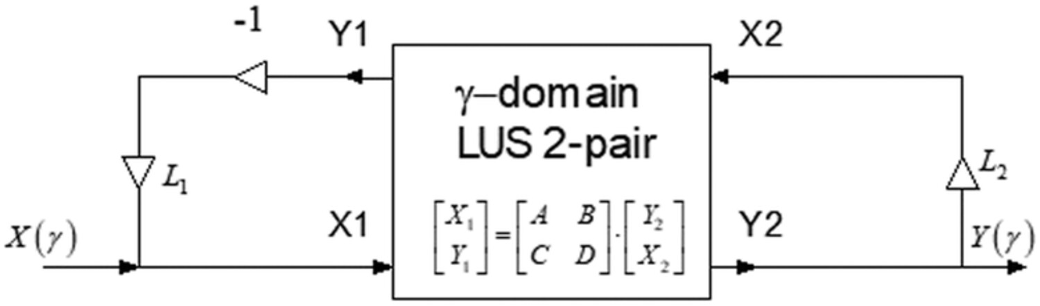
The theory of the delta discrete-time operator-based doubly terminated two-pair (ladder) is presented here for use in sampled-data and digital filter design. The two-pair filter utilizes traditional forward Euler and backward Euler integrators, is lossless under scaling (LUS), and possesses good magnitude sensitivity which is induced intrinsically due to the filter structure.
Energy efficient approximate booth multipliers using compact error compensation circuit for mitigation of truncation error
- Pages: 2252-2270
- First Published: 25 February 2022
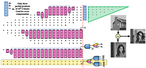
Highly compact approximate multipliers.
Shared reduced ordered binary decision diagram-based thermal-aware network synthesis
- Pages: 2271-2286
- First Published: 01 March 2022
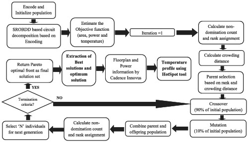
In this work, thermal-aware realization of a combinational logic network has been discussed. Input variable ordering of shared reduced ordered binary decision diagram is done using nondominated sorting genetic algorithm-II (NSGA-II). Using this technique, an effort is made to co-optimize temperature, area, and power simultaneously. MCNC benchmark circuits are tested using the proposed approach and an improvement of 13.65% in the silicon area and up to 10% in power dissipation, and 2.72% peak temperature reduction is reported in comparison with existing literature.
CORRIGENDUM
Sign up for email alerts
Tools
More from this journal:
This journal supports the Wiley Research Diversity, Equity & Inclusion statement
Read the statement