Configurable Transmitter and Systolic Channel Estimator Architectures for Data-Dependent Superimposed Training Communications Systems
Abstract
In this paper, a configurable superimposed training (ST)/data-dependent ST (DDST) transmitter and architecture based on array processors (APs) for DDST channel estimation are presented. Both architectures, designed under full-hardware paradigm, were described using Verilog HDL, targeted in Xilinx Virtex-5 and they were compared with existent approaches. The synthesis results showed a FPGA slice consumption of 1% for the transmitter and 3% for the estimator with 160 and 115 MHz operating frequencies, respectively. The signal-to-quantization-noise ratio (SQNR) performance of the transmitter is about 82 dB to support 4/16/64-QAM modulation. A Monte Carlo simulation demonstrates that the mean square error (MSE) of the channel estimator implemented in hardware is practically the same as the one obtained with the floating-point golden model. The high performance and reduced hardware of the proposed architectures lead to the conclusion that the DDST concept can be applied in current communications standards.
1. Introduction
Presently, there is need to develop communications systems capable of transmitting/receiving various types of information (data, voice, video, etc.) at high speed. Nevertheless, designing these systems is always an extremely difficult task, and, therefore, the system must be broken down into several stages each with a specific task. The complexity of each stage is higher when the system operates in a wireless environment because the additional challenges that should be facing due to the complex nature of the channel and its susceptibility to several types of interference.
As it is not possible to avoid the influence of the channel on a transmitted data sent through it, an option is to characterize the channel parameters with enough precision so that their effects can be reverted in the receiver. For that reason, channel estimation stage is a key part of any reliable wireless system because a correct channel estimation leads to a reduction of the bit error rate (BER). The channel estimator must deal with multiple phenomenas, such as multipath propagation and frequency Doppler (due to the mobility of the users). In order to deal with these problems, current communication standards specify the transmission of pilot signals which are known in the receiver, allowing an ease estimation of the communication channel. The way of transmitting such pilot signals can be classified in to two major branches: pilot-assisted transmission (PAT)—where pilot and data signals are multiplexed in time, frequency, code, space, or in a combination of the mentioned domains—and implicit training (IT), a technique proposed recently where the pilot signal is hidden in the data transmitted. PAT is the technique implemented in actual standards, such as WiMAX, WiFi, and Bluetooth. It presents the advantage that pilots and data relies on orthogonal subspaces allowing a simple separation of them in the receiver; however, it is necessary to decrease the available bandwidth for data in order to transmit the pilot signal. On the other hand, IT overcomes this problem because all the time, data and pilot signal are transmitted; nevertheless, it leads to a transmission of such signals into nonorthogonal subspaces. Despite the aforementioned, IT has been recognized as a feasible alternative for future communication standards [1].
The simplest form to carry out IT is to add (superimpose) the pilot signal to the data. This approach is known as superimposed training (ST), first proposed in [2] and enhanced by diverse authors whose results are summarized in [3, Ch. 6]. In [4–8] was presented a refinement of ST known as data-dependent superimpose training (DDST), this technique makes it possible to null the interference of data during the estimation process via the addition of a new training sequence, which depends on the transmitted data, together with the data and the ST sequence.
Because of the benefits that ST/DDST offer, it is necessary to develop efficient implementations of these algorithms. Although these techniques have been widely studied, to this point, there exist few reported practical implementations in the literature. In fact, almost all of them are approximations based on floating point and software. In [9], the algorithms are programmed in a digital signal processor (DSP) for a low-rate communication system, while in [10] the proposed implementation is developed into an embedded microprocessor with hardware accelerators inside of a FPGA. At ReConFig 2011, we have presented a full-hardware architecture—with high throughput, low hardware consumption, and high degree of reusability—for the channel estimation stage of an ST/DDST receiver [11]. Its novelty consisted in that a systolic array processors (AP) was used for performing the entire estimation process instead of two separated signal processing modules. In this paper, we present a extended version of that paper, where a hardware-efficient architecture for configurable ST/DDST transmitter that supports 4/16/64-QAM constellations is used to complement the results presented in [11], because now, all transmitted data—in each Monte Carlo trial—are generated by the proposed transmitter hardware instead of the transmitter simulation model programmed in Matlab.
The rest of the paper is organized as follows. Section 2 presents the system model being considered, the ST/DDST transmitter structure, the channel estimation algorithm, and the cyclic mean reformulation onto systolic APs. Section 3 describes in detail the full-hardware architectures for the configurable ST/DDST transmitter. Section 4 proposes an architecture based on SA processor for the DDST channel estimator. In Section 5, the performance evaluation of the proposed architectures is carried out. Conclusions are set down in Section 6.
Notation 1. Lowercase (uppercase) bold letters denote column vectors (matrices). Operators (A) H, (A) T, and (A) −1, denote the Hermitian, transpose, and inverse operations of matrix A. 1n represents a column vector of length n with all its elements equal to one; similarly, 0n represents an all-zeros column vector of length n. In is the identity matrix of size n × n. [a] k denotes the kth element of vector a. [a] m:n denotes a vector conformed with the elements of a as follows: [[a] m, [a] m+1, …, [a] n] T. ⊗ represents Kronecker product. Finally, E(·) represents the expectation operator.
2. System Model
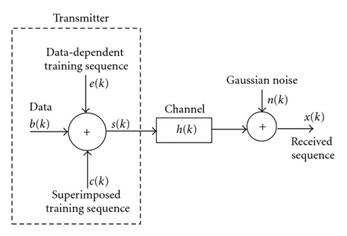
This section is devoted to introduce the DDST algorithm mentioned previously. Suppose a single carrier, baseband communication system based on DDST as the one presented in Figure 1. The transmitted signal x(k) conformed to the sum of the data sequence b(k), the training sequence c(k) and the data-dependent training sequence e(k). The index k helps to enumerate the samples of such signals which are transmitted at a rate equal to 1/T. c(k), is a periodic sequence with period equal to P and power equal to [12]. It is assumed that the data sequence is a zero-mean, stationary stochastic process with power equal to , where the symbols of such process come from a equiprobable alphabet. The sequence e(k) is constructed as mentioned in [5]. s(k) is propagated through the communication channel h(k) whose time impulse response conformed to the convolution of the system filters and the propagation medium impulse responses (all of them assumed to be time-invariant). Such channel can be modeled as a finite impulse response (FIR) filter with L time-invariant coefficients as much. Finally, the distorted signal by the channel is contaminated with the noise n(k) for conforming the received signal x(k). n(k) is a zero-mean white Gaussian noise, which possess variance equal to . The transmission of blocks of N symbols, which is preceded by a cyclic prefix of length CP ≥ L is assumed. Perfect block synchronization, which allows to fix P = L it is also assumed. For ease of implementation, it is assumed that N is a multiple of P and P is a power of two.
2.1. Digital Transmitter with ST/DDST Included

2.2. Channel Estimation Using DDST
2.3. Cyclic Mean Algorithm Using Array Processors and Partitioning
Therefore, the array of PEs will process one pair of B and 1P blocks after another in a sequential manner together with partial results.
3. A Configurable ST/DDST Transmitter Architecture
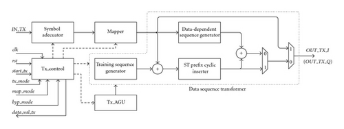
Considering the explained in Section 2.1, the architecture shown in Figure 3 is proposed for the transmitter. It is composed of the five hardware modules: the symbol adecuator, the mapper, the data sequence transformer, the Tx_control, and the Tx_AGU. The reconfigurability feature of the architecture allows to switch between two operating modes: ST or DDST, in order to send data blocks with a cyclic prefix attached. In both modes, the transmitter hardware supports 4/16/64-QAM constellations.
In the next subsections, additional details about the main transmitter modules will be described.
3.1. Symbol Adecuator
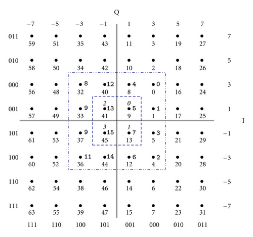
The design of this module is widely conditioned by the features of the mapper. By early account, a key aspect exploited in the mapper design, it consists of the fact that the 4-QAM and 16-QAM constellations are contained in Grey-coded 64-QAM one, as shown in Figure 4. For that reason, the symbol adecuator is necessary because not all the same point-numbers in the three constellations are mapped to the same complex symbol output. For example, while the point number 2 of the 4-QAM constellation is mapped to −1 + j symbol, 16-QAM will map this point number to 3 − 3j and 64-QAM will map to 3 + 5j.

3.2. Mapper
3.3. Data Sequence Transformer
The data sequence transformer is the greater complexity module of the transmitter. Thus, its design was broken down into three submodules, whose individual architectures are described in the following paragraphs.
3.3.1. Training Sequence Generator
Analyzing (4), it can be noticed that the parameters , N, and P, needed to generate the training sequence, are known in advance and they remain constants during the transmitter operating. Hence, the P values of the training sequence can be calculated off-line, quantized, and stored in an LUT. This LUT is read NP times in order to expand the training sequence length, as indicated in (3), and it can be superimposed, element by element, with the data sequence by the complex adder.
3.3.2. ST Cyclic Prefix Insertion Submodule
- (i)
Since the prefix cyclic conformed to the last P data of the sequence ST, it can only be generated from this sequence until it has been completely processed.
- (ii)
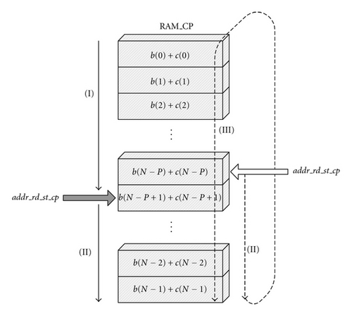
Given that, in all the N + P data to be transmitted, the first P data correspond to the cyclic prefix, it is necessary to use a memory buffer in order to store the remaining N data (ST sequence) and, thus, prevent data loss.
- (I)
When the (N − P + 1)th datum is stored in RAM_CP, the previous datum stored is addressed by addr_rd_st bus.
- (II)
During P clock cycles, the ST sequence storing and reading take place in the RAM_CP.
- (III)
The ST sequence storing in the RAM_CP is stopped. However, the data reading will continue for N cycles.
3.3.3. Data-Dependent Sequence Generator
- (I)
The b(k) sequence is rearranged into a matrix of size P × NP, according to
(19) - (II)
The mean of the each rows of the matrix B is obtained.
- (III)
The P mean results are replicated NP + 1 times in order to obtain the e vector and P data for DDST cyclic prefix purposes.
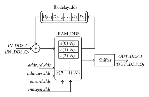
Figure 7 shows the hardware architecture of DDS generator. Its novel design avoids the b(k) sequence rearranging by the loop-back shift register lb_delay_dds. This register generates a P symbol delay in order to align the data for each B matrix row. So, the data rows can be added “on the fly” by the complex adder without the data input stream is stopped. The sum results are stored in the RAM_DDS, after its entire contents are read NP + 1 times and each datum is divided by NP in the shifter block. Finally, the results are sent to the DDS generator outputs.

4. Systolic Channel Estimator Architecture
This section introduces an architecture for the DDST-based channel estimation process. Its design is based on MVM operation, which is carried out in a systolic way into AP. The main idea in the system design is to reuse the same systolic array for computing the cyclic mean of the received data. The proposed architecture, called in this paper “systolic DDST channel estimator” (SYSDCE) is depicted in Figure 8(a). Four functional units can be identified: a modified systolic matrix-vector multiplier (MSYSMVM), a data input feeder (DATINF), an inverse C look-up table (ICLUT), and a control unit (CU). Broadly speaking, the SYSDCE operation can be divided into three phases: input sequence storage, cyclic mean compute, and CIR estimate.
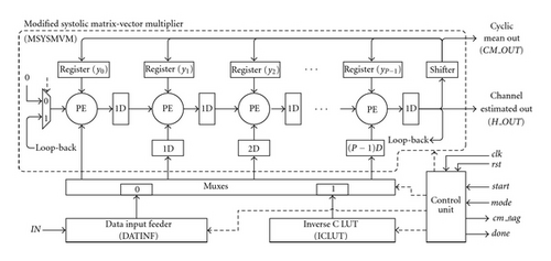
As soon as the start signal is asserted, an N + P data samples (vector x and cyclic prefix, resp.) can be read from the input port IN. After excluding the samples corresponding to the cyclic prefix, the rest of samples are rearranged and stored in the memory bank of DATINF. When this process is finished, the CU configures the MSYSMVM unit and during NP cycles it reads P parallel data per cycle from DATINF and computes the cyclic mean y. Once this phase is finished, the obtained vector y together with ICLUT data are fed to the MSYSMVM again for performing the product expressed in (10). Finally, after P + 1 cycles, the done flag is asserted and one by one the coefficients of the channel estimated are sent to the bus H_OUT. It is worth mentioning that the SYSDCE can be configured to compute only the cyclic mean if mode input control signal has been set to zero. In this case, the cm_flag out is asserted to indicate that valid results are available in CM_OUT bus. Thus, the channel estimator is prepared for another data sequence processing. A deeper explanation about each component of the SYSDCE architecture will be given in the subsections.
4.1. Modified Systolic Matrix-Vector Multiplier (MSYSMVM)
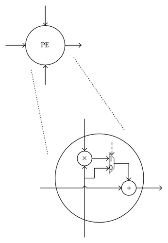
The fundamental operation to perform by SYSDCE is a matrix-vector multiplication which is high time-processing demanding. The hardware design for solving this operation is the most critical part in the architecture. The obvious strategy for accelerating MVM consists in computing as many operations as possible, with the penalty of a great consumption of FPGA resources. Therefore, this paper proposes a modification of the systolic MVM presented in [14, Ch. 3] in order to obtain a good performance with reasonable resources consumption. This modification allows to compute the cyclic mean using partitioning method with the same systolic array reported. Figure 8(b) shows the processor element (PE), which is the atomic digital signal processing module in MSYSMVM. It processes three flows: the data flow from the ICLUT or DATINF, the input registers values, and the data produced by the previous adjacent PE.
In the MSYSMVM design was considered that the number of PEs needed (AP size) is P, which matches with the dimensions of matrix Γ and vector y, respectively. The projection vector d = [1 0] T (see details in [14]) was used with a vector schedule s = [1 1] T. The pipelining period for this design is equal to 1 and the computing time for the full MVM is 2P − 1 clock periods.
For computing the cyclic mean using the MSYSMVM module, the original structure of PE was modified with an additional multiplexer. For that reason, the PE can perform all trivial multiplications by bypassing the data from the input of the complex multiplier directly to the complex adder.
4.2. Data Input Feeder (DATINF)
Similar to almost any systolic array, the MSYSMVM needs the data, which will be fed to each of its PEs to be given in a defined order before processing it. In the proposed approach, the module DATINF is responsible for performing this task. It is made up of an array of P memories, each with a depth of NP, organized as a memory bank as shown in Figure 9. DATINF reads N + P data from IN bus; it identifies and removes the first P data corresponding to CP. Subsequently, this module rearranges this sequence (correspondence to x(k)) in NP/P blocks of size P × P in order to form . Therefore, the N stored data can be viewed as a NP × P matrix, where each individual memory in the bank stores one column of each block and the blocks are stored consecutively one after another, as depicted in Figure 9.
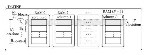
In order to minimize the hardware consumption, a “hard-wired” addressing approach was built for the memory bank. As shown in Figure 10, the log2(N) bits corresponding to the DATINF address bus are split into three parts. The first log2(N/NP) most significant bits (MSB) are used for block selecting, the next log2(NP/P) MSB are used to select a particular memory in the bank and the remaining log2(P) bits are used to individually address each of the locations in the selected memory.

4.3. Inverse C Look-Up Table (ICLUT)
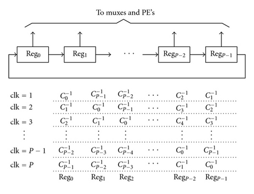
The values of the circulant matrix C−1 are constants that can be precomputed once off-line and stored in a LUT. Only the values of the first column are necessary because the remaining columns are shifted versions of the first one. Consequently, the ROM location’s number required for the LUT is just P. If traditional design is used, then the LUT will be designed with a multiport ROM of P locations, but it will be synthesized by the employed compiler tool as an array of P single-port ROMs. Therefore, the number of memory locations is increased to P2. A novel solution was designed with an array of P registers operating as a circular buffer. This is called “inverse C look-up table” (ICLUT) and it saves P(P − 1) memory locations. The first row values of C−1 are stored in the registers. Next, one rotation is applied in each tick of the clock to change the register’s outputs, as indicated in Figure 11.
5. Results
In this section, the proposed architectures are evaluated. First, the hardware utilization and throughput of the ST/DDST transmitter implementation are presented. After, its functional performance from the point of the signal-to-quantization-noise ratio (SQNR) is analyzed. Next, the FPGA resources consumption and throughput of the SYSDCE implementation are obtained. Finally, the SYSDCE functional results specified in terms of the MSE of the channel estimated and SQNR performance are carried out by Monte Carlo simulations and using the transmitter hardware in DDST mode.
5.1. Implementation and Simulation of the Transmitter
The configurable ST/DDST transmitter architecture was implemented in RTL level using Verilog hardware description hardware. It is able to transmits ST or DDST data blocks of length N with CP = P. The power of training sequence is set to with a period P = 8. The configurable transmitter was synthesized and targeted in Xilinx Virtex-5 XC5VLX110T FPGA. Default settings and no “user constraints” were selected in the EDA tool Xilinx ISE v11. No IP core o predesigned component were used. All signals are represented in signed fixed-point two’s complement, and nonrounding scheme was considered.
Table 1 summarizes the synthesis results for the proposed ST/DDT transmitter. Analyzing this table, it can be noted a operating frequency of 160 MHz with a symbolic FPGA resource utilization. So, it is clear that excellent area-frequency balance is achieved.
| FPGA resource | Used | Available | Utilization |
|---|---|---|---|
| Frequency | 160.12 | MHz | — |
| Slice registers | 141 | 69120 | <1% |
| Slice LUTs | 437 | 69120 | <1% |
| Fully used LUT-FF pairs | 134 | 444 | 30% |
| IOBs | 46 | 640 | 7% |
| BRAMs | 4 | 148 | 2% |
On the other hand, it is difficult to compare directly the proposed transmitter and channel estimator with the others previously presented in [9, 10] because of the differences in technology, paradigms used, and testing conditions. In [9], DDST communication system was implemented under full-software philosophy in TMS320C6713 DSP with a 300 MHz external clock. A hybrid software-hardware FPGA implementation of the DDST receiver is described in [10]. In both DDST implementations mentioned, the comparison against our transmitter was not possible. In the former because the transmitter was full-software based and the latter only the DDST receiver was implemented.
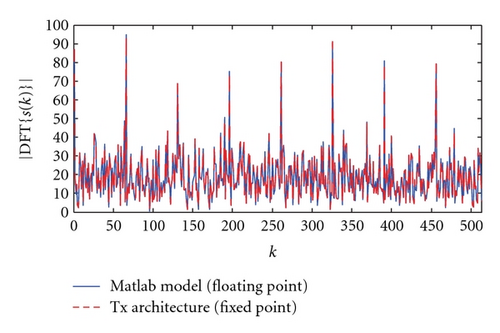
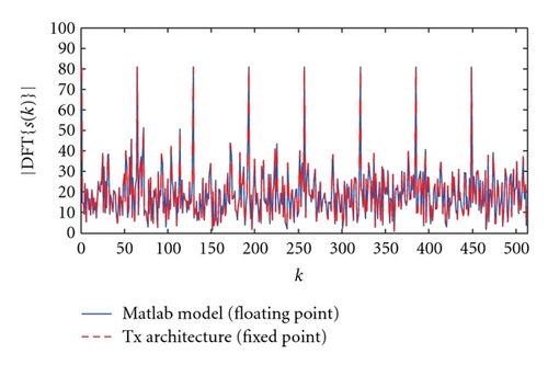
The transmitter operating validity is presented in Figure 12. The first graph (Figure 12(a)) shows clearly that the transmitter hardware has embedded the training sequence c(k) into b(k). It can be noted that the data sequence energy is spread in all frequency components. In contrast, the training sequence energy are only concentrated in P equispaced frequency components. Similar behavior occurs in the DDST mode (Figure 12(b)), but now the pilots signals also have the same energy. This is unequivocal proof that the transmitter architecture is properly superimposing c(k) and e(k) into b(k).
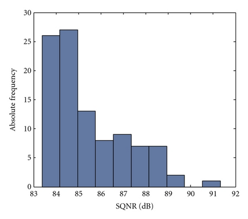
The SQNR obtained for 100 Monte Carlo trials is monitored, in order to quantify the difference between the s(k) sequence obtained with the hardware transmitter compared with the floating-point transmitter golden model. Thus, the histogram of Figure 13 represents concisely the results of this test. The most of the occurrence are concentrated in 84 dB.
5.2. Implementation and Simulation of the Channel Estimator
The SYSDCE architecture was implemented using the same considerations and design parameters of the transmitter. Also, the systolic channel estimator was synthesized and targeted in the same FPGA.
Table 2 summarizes the synthesis results for the proposed estimator. The values in the parenthesis in each feature indicate the total of corresponding available resources in the FPGA. The results in Table 1 reveal a frequency operation of 115.247 MHz with a minimal consumption (except DSP48Es) with respect to the total resources of the FPGA.
| Input length (without CP) | (N) | 512 |
| Frequency | (MHz) | 115.247 |
| Slice registers | (69120) | 1370 (1%) |
| Slice LUTs | (69120) | 2587 (3%) |
| Fully used LUT-FF pairs | (3348) | 609 (18%) |
| Block RAMs | (148) | 8 (5%) |
| DSP48Es | (64) | 32 (50%) |
Againly, it was not possible to compare the SYSDCE against the existent approaches. In [10], the module corresponding to the channel estimation, only the arithmetic mean was accelerated by a dedicated coprocessor. In this work, the input sequence length was assumed (but it did not explicitly mentioned) to be N = 512 symbols. The MVM operation described in (9) was implemented in software. Also, no results—from the point of view of the mean square error (MSE) in the channel estimated or SQNR performance—are presented.
| Channel estimator | Input length | Cycles/estimation | CT (us) | TP (MS/s) | TP/area (MS/s/ slices) |
|---|---|---|---|---|---|
| SYSDCE (cyclic mean mode) | 512 | 591 | 5.128 | 101.40 | 25.625e3 |
|
512 | 606 | 5.258 | 98.91 | 24.996e3 |
| Arithmetic mean coprocessor in [10] | 512 | 2238 | 20 | 26.39 | NA |
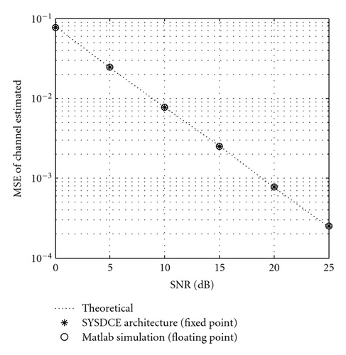
The validity of the provided architectures is granted by comparing their results with the floating-point simulation golden model programmed in Matlab, in terms of channel estimation error versus signal-to-noise ratio (SNR). Thereby, the following scenario (similar to that used in [6]) was considered. The hardware transmitter was configured in DDST mode, in order to send data blocks of N = 512 symbols obtained from a 4 QAM constellation. The channel is randomly generated at each Monte Carlo trial and it is assumed to be Rayleigh with length L = 8. The power of training sequence is set to with a period P equal to L.
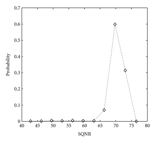
Figure 14 shows the MSE of channel estimated, which is averaged over 300 Monte Carlo simulations for each value of SNR. Note that the MSE of the hardware estimator is too close to the theoretical line [4] and almost indistinguishable with respect to the golden model. On the other hand, Figure 15 presents the probability density function (PDF) of the SYSDCE hardware, obtained for the same Monte Carlo trials. Analyzing such PDF, it can be noted that the fixed-point performance in average is about 68 dB in terms of SQNR.
6. Conclusions
In this paper, digital architectures for transmitter and channel estimation stages of the ST/DDST communications systems have been presented. These architectures represent the first implementations under the full-hardware philosophy for a wireless systems based on ST/DDST. Both architectures present high throughput and reduced FPGA resources consumption, achieving a good trade-off between performance and area utilization. The proposed transmitter architecture is configurable enough to generate two types of training using three constellation orders. In the SYSDCE hardware, it is possible to observe a great flexibility and reusability because the same systolic array is used for two different tasks (operations): cyclic mean and channel estimation. Also, the SYSDCE design can be easily modified (by means of partitioning strategy) for processing channels of different lengths. The validity and performance of these approaches have been verified by Monte Carlo simulations, where an SQNR of 82 dB and 68 dB in average are achieved for the transmitter and the SYSDCE, respectively. At the same time both architectures present a insignificant differences in the performance results when they are compared with their respective floating-point golden models. The provided results show that ST/DDST concepts can be effectively utilized in current and future wireless communications standards.
Acknowledgments
This work was supported by PROMEP ITSON-92, CONACYT-181962, and Mixbaal 158899 Research Grants.


