Multi-Softcore Architecture on FPGA
Abstract
To meet the high performance demands of embedded multimedia applications, embedded systems are integrating multiple processing units. However, they are mostly based on custom-logic design methodology. Designing parallel multicore systems using available standards intellectual properties yet maintaining high performance is also a challenging issue. Softcore processors and field programmable gate arrays (FPGAs) are a cheap and fast option to develop and test such systems. This paper describes a FPGA-based design methodology to implement a rapid prototype of parametric multicore systems. A study of the viability of making the SoC using the NIOS II soft-processor core from Altera is also presented. The NIOS II features a general-purpose RISC CPU architecture designed to address a wide range of applications. The performance of the implemented architecture is discussed, and also some parallel applications are used for testing speedup and efficiency of the system. Experimental results demonstrate the performance of the proposed multicore system, which achieves better speedup than the GPU (29.5% faster for the FIR filter and 23.6% faster for the matrix-matrix multiplication).
1. Introduction
The requirements for higher computational capacity and lower cost of future high-end real-time data-intensive applications like multimedia and image processing (filtering, edge detection, correlation, etc.) are rapidly growing. As a promising solution, parallel programming and parallel systems-on-a-chip (SoC) such as clusters, multiprocessor systems, and grid systems are proposed. Such sophisticated embedded systems are required to satisfy high demands regarding energy, power, area, and cost efficiency. Moreover, many embedded systems are required to be flexible enough to be reused for different software versions. Multicore systems working in SIMD/SPMD (Single Instruction Multiple Data/Single Program Multiple Data) fashion have been shown to be powerful executers for data-intensive computations [1, 2] and prove very fruitful in pixel processing domain [3, 4]. Their parallel architecture strongly reduces the amount of memory access and the clock speed, thereby enabling higher performance [5, 6]. Such multicore systems are made up of an array of processing elements (PEs) that synchronously execute the same program on different local data and can communicate through an interconnection network. These parallel architectures are characterized by their regular design, which enables design-cost effective scaling of the platform for different performance applications by simply increasing or reducing the number of processors. Although these architectures have accomplished a great deal of success in solving data-intensive computations, their high price and the long design cycle have resulted in a very low acceptance rate [7]. Designing specific solutions is a costly and risky investment due to time-to-market constraints and high design and fabrication costs. Embedded hardware architectures have to be flexible to a great extent to satisfy the various parameters of multimedia applications. To overcome these problems, embedded system designers are increasingly relying on field programmable gate arrays (FPGAs) as target design platforms. Recent FPGAs provide a high level of logic element density [8]. They are replacing ASICs (Application Specific Integrated Circuits) in many products due to their increased capacity, smaller nonrecurring engineering costs, and programmability [9, 10]. It is easy to put many cores and memories on an FPGA device, which today has over 100 million transistors available. Such platforms allow creating increasingly complex multiprocessor system-on-a-chip (MPSoC) architectures. FPGAs also support the reuse of standard or custom IP (intellectual property) blocks, which further decreases system development time and costs. A good example is the use of softcores, such as the NIOS II [11] and the MicroBlaze [12] for Altera and Xilinx FPGAs, respectively, to implement FPGA-based embedded systems. Thus, the importance of multicore FPGAs platforms steadily grows since they facilitate designing parallel systems. Based on configurable logic (softcores), such systems provide a good basis for parallel, scalable, and adaptive systems [13].
In a context of high performance, low technology cost, and application code reusability objectives, we target FPGA devices and softcore processors to implement and to test the proposed multicore system. The focus of this work is to study the viability of softcore replication design methodology to implement a multicore SPMD architecture dedicated to compute data-intensive signal processing applications. Three benchmarks that represent different application domain were tested: FIR filter, spatial Laplacian filter, and matrix-matrix multiplication, characteristic for 1D digital signal processing, 2D image filtering, and linear algebra computations, respectively. All tested applications involve the computation of a large number of repetitive operations.
The remainder of this paper is organized as follows. The next section briefly introduces the multicore system with focus on the proposed FPGA-based design methodology. In Section 3, the main characteristics of the NIOS II softcore processor are presented. The methodology followed to adapt the NIOS II IP to the parallel SoC requirements is also described. Section 4 discusses some experimental results showing the performance of the softcore-based parallel system. Section 5 gives an overview of related work. A performance analysis and comparison of the implemented system with other architectures and a discussion on the architectural aspects are also provided. Finally, Section 6 presents the concluding remarks and further work.
2. Softcore-Based Replication Design Methodology
In this section, we first give an overview over our multicore architecture including the different used components. Then, we describe the replication design methodology based on the use of the NIOS II softcore as a case study.
2.1. Multicore SoC Overview
The proposed parallel multicore system works in SPMD fashion.
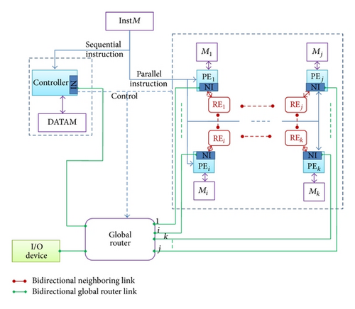
All processors execute the same instructions coming from a parallel instruction memory (InstM). The controller serves as a master and can only execute sequential program whereas each PE executes the same parallel program while operating on its local data. The execution of a given instruction depends on the activity of each PE, identified by a unique number in the array. In fact, each processor in the multicore system is characterized by its identity to specify its own job. The multiple processors can communicate via two types of networks: a neighbourhood network and a crossbar network (global router) that assures point-to-point communications between processors and also performs parallel I/O data transfer. The neighbourhood network interconnects the PEs in a NEWS fashion so that every PE can communicate with its nearest neighbour in a defined direction (north, south, east, or west). It mainly consists of a number (equal to the number of PEs) of routing elements (RE) which are arranged in a grid fashion and are responsible of routing the data between PEs. The routers may be customized at compile time to implement three different topologies (Mesh, Torus, and Xnet). It is also possible to change dynamically from one topology to another according to the application needs. The global router assures the irregular communications between the different components and can be configured in four possible bidirectional communication modes: PE-PE, PE-Controller, PE-I/O Peripheral, and Controller-I/O Peripheral. These different described communication patterns are handled by the communication instructions (presented in Section 3.2) as defined by the designer. To achieve the required architecture performance and configurability, a fully parameterizable and structural description of the networks of the proposed architecture was done at the RTL (Register Transfer Level) using the VHDL (Very High Speed Integrated Circuits Hardware Description Language).
The proposed multicore SoC is a parameterizable architecture template and thus offers a high degree of flexibility. Some of its parameters can be reconfigured at synthesis time (such as the number of PEs as well as the memory size), whereas other parameters can be reconfigured at runtime like the neighbourhood network topology. Table 1 details these different parameters.
| Parameters | Time | Values | Default value |
|---|---|---|---|
| Number of PEs | Design | 2N, N > 0 | 24 |
| Size of PE local memory | Design | Limited by the FPGA surface | 5 KB |
| Neighborhood network’s topology | Design and runtime | Mesh, Torus, and Xnet | Torus |
| Global router communication mode | Runtime |
|
PE-Controller |
This multicore prototype serves as a base to test different configurations with different processors. The designer just needs to use a given processor IP and adapt the network interface to that processor. Such characteristics make the system scalable and flexible enough to satisfy a wide range of data-parallel applications needs.
The following subsection highlights the FPGA-based replication design methodology followed to build the multicore system. A case study is then highlighted based on the NIOS II softcore.
2.2. Design Approach
To design a parallel multicore SoC, we propose in this paper a replication design methodology, which consists in using a softcore to implement the different processors in the multiprocessor array. Following this manner, the design process is easier and faster than traditional design methods. As a consequence, it offers a large gain in the development time. The additional advantage of this methodology is the facility of programming since we use the same instruction set for all processors. The aim is to propose a flexible, programmable, and customizable architecture to accelerate parallel applications.
Figure 1 illustrates the multicore architecture based on the replication design methodology. The designer has to carefully respect the system requirements in order to integrate a given processor IP. In the proposed system, the controller is in charge of controlling the global router functioning and transferring or reading data to or from PEs respectively. The PE executes parallel instructions and communicates with neighbouring PEs through the neighbourhood network or with the controller and peripherals through the global router. To accomplish these different functionalities, the controller has to be interfaced with the global router whereas the PE has to be interfaced with the neighbouring network as well as the global router (as shown in Figure 1). In both cases, the networks only need data and address signals issued from the different processors. Table 3 details the global router network interface with the processors. It is scalable so that it is adapted to a parametric number of PEs. This is performed by mapping each PE data and request to input ports configured as a vector of length equal to the number of PEs. The neighbourhood network interface only contains data and addresses coming or going to PEs. It consists of a number of routers (equal to the number of PEs), each one connected to one PE. Connections between the routers allow transferring data through several paths across the architecture. Both implemented on-chip networks are reliable, in the sense that data sent from one core is guaranteed to be delivered to its destination core. The results obtained for the network interface hardware cost, on the Stratix V FPGA [14], are summarized in Table 2.
| Neighbourhood network | Global router | |||
|---|---|---|---|---|
| NI | Area occupancy | NI | Area occupancy | |
| ALUTs | 36 | 0.0077% (36/469 440) | 2 | 0.0004% (2/469 440) |
| Registers | 118 | 0.0125% (118/938 880) | 75 | 0.0079% (75/938 880) |
| In | ||
|---|---|---|
| pe_d_in | [k] [32 b] | PE data (32-bit data vector (length = number of PEs)) |
| pe_a_in | [k] [32 b] | PE address (32-bit address vector (length = number of PEs)) |
| pe_wr | [k] [1 b] | PE read/write (1-bit R/W vector (length = number of PEs)) |
| Ctrl_d_in | [32 b] | Controller data (32 bits) |
| Ctrl_a_in | [32 b] | Controller address (32 bits) |
| Ctrl_wr | [1 b] | Controller read/write signal |
| Out | ||
| pe_d_out | [k] [32 b] | PE data out |
| pe_a_out | [k] [32 b] | PE address |
| Ctrl_d_out | [32 b] | Controller data out |
| Ctrl_a_out | [32 b] | Controller address out |
| I/O Peripherals | ||
| SRAM_d_out | [32 b] | SRAM data out |
| SRAM_a_out | [32 b] | SRAM address out |
| SDRAM_d_in | [32 b] | SDRAM data in |
| SDRAM_a_in | [32 b] | SDRAM address |
| Acc_d_in | [32 b] | HW accelerator data in |
| Acc_a_in | [32 b] | HW accelerator address in |
It is remarkable from the synthesis results given in Table 2 that the implemented network adapters present a cheap solution requiring a significant small logic area on the FPGA. This demonstrates the simplicity of the interface and confirms that changing the processor IP is an easy task. Thus, small design time is required to reconfigure the architecture.
The next section discusses more precisely the use of the NIOS II IP to implement a multicore configuration following the replication methodology.
3. NIOS II-Based Multicore Architecture Overview
3.1. Architecture Description
The NIOS II embedded softcore is a reduced instruction set computer, optimized for Altera FPGA implementations. A block diagram of the NIOS II core is depicted in Figure 2 [11].
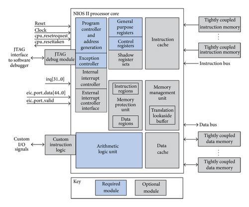
It can be configured at design time (data width, amount of memory, included peripherals, etc.) in order to be optimized for a given application. The most relevant configurations are the clock frequency, the debug level, the performance level, and the user-defined instructions. The performance level configuration enables the user to choose one of the three provided processors: the NIOS II/fast, which results in a larger processor that uses more logic elements but is faster and has more features; the NIOS II/standard, which creates a processor with balanced relationship between speed and area and some special features; the NIOS II/economic, which generates a very economic processor in terms of area, but very simple in terms of data processing capability.
In this work, we use the NIOS II economic version in order to put a large number of processors in one FPGA device since we target a multicore SoC. NIOS II processors use Avalon bus for connecting memories and peripherals. So, the implemented network interface is based on Avalon interface. The Avalon interface is basically an interface that creates a common interface from different interfaces of all memory and peripheral components of the system. In this work, we use the Avalon-Memory Mapped interface (Avalon-MM) [15]. It is an address-based read/write interface synchronous to the system clock. A wrapper, considered as the network interface, has been implemented in order to be able to integrate the NIOS with other components of the architecture, mainly the neighbourhood network and the global router. This wrapper is a custom component which has two interfaces: one Avalon slave interface to be connected to the NIOS and one conduit interface (for exporting signals to the top level) to be connected to the networks. To assure communication, we only need addresses and data coming from processors as well as the read/write enable signal to indicate if it is a read or write operation. The NIOS-based wrapper is responsible of transferring data and addresses of the attached processor to the appropriate network (dependently on the address coding). Moreover, it communicates the data and addresses received from networks to the processor depending on its identity number.
To design systems which integrate a NIOS II processor, Quartus II has as complement a SW called Qsys [16]. Qsys is used to specify the NIOS II processor cores, memory, and other components the system requires. Qsys automatically generates the interconnect logic to integrate the components in the hardware system. The NIOS II-based SoC synthesis flow is summarized in Figure 3.
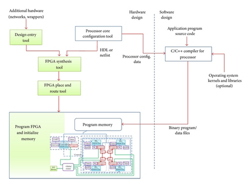
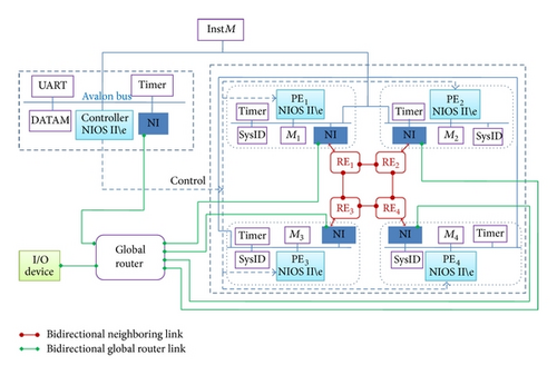
In the implemented architecture, each processor is connected to a timer which provides a periodic system clock tick, a system ID peripheral which allows uniquely identifying the PE, and to a local data memory. In addition, the controller is connected to a JTAG UART which allows communicating PC with the NIOS core through the USB-Blaster download cable and providing debug information. Each processor is also connected to a custom peripheral which integrated the network interface, allowing transferring the processor requests to the other components in the multicore architecture.
An example of 4-core architecture is shown schematically in Figure 4. In the architecture, different subsystems are connected by network interfaces (NI) to networks (neighbourhood network and global router). A network interface is used to send and receive data transmitted over the network. Each subsystem contains the processor and some peripherals or accelerators. The total number of PEs, defined by the number of rows and columns, can be specified before synthesis.
The design steps followed to implement the multicore architecture show the simplicity of the replication methodology to be applied on any softcore processor and the configurability of the proposed SoC prototype. To build a multicore system, two steps have to be performed: to adapt the network interface to be connected to the chosen processor and to define the corresponding communication instructions based on the processor instructions since the HW networks are managed by the SW program. The latter step is more detailed in the next paragraph.
3.2. SW Programming
- (i)
MODE instruction allows setting the needed communication mode and is executed by the controller: IOWR (NI_BASE, 0x800, data), where data is the value that corresponds to the global router communication mode (PE-PE, PE-Controller, PE-I/O Peripheral, or Controller-I/O Peripheral) as defined in the multicore architecture configuration file.
- (ii)
SEND instruction allows sending data through the global router: IOWR (NI_BASE, address, data), where NI_BASE is the address of the controller network interface based custom component when the instruction is executed by the controller or the PE network interface based custom component when it is executed by the PE. The address field (11 bits) contains the following:
- (1)
the identity of the PE receiver (mode PE-PE, mode Controller-PE, and mode I/O Peripheral-PE);
- (2)
“00000000000” (mode PE-Controller and mode I/O Peripheral-Controller);
- (3)
the peripheral address (mode PE-I/O Peripheral and mode Controller-I/O Peripheral).
- (1)
- (iii)
RECEIVE instruction allows receiving data through the global router: data = IORD (NI_BASE, address). It analogously takes the same address field as the SEND instruction.
In the case of the neighbouring communication, SEND and RECEIVE instructions are also encoded from IORD and IOWR NIOS macros. Compared to the global router instructions, they only differ in the address field, which contains the direction to which the data will be transferred (0: north, 1: east, 2: west, 3: south, 4: northeast, 5: northwest, 6: southeast, and 7: southwest).
Altera provides the NIOS Integrated Development Environment tool to implement and compile the parallel SW program. The following section presents the implementation and experimental results of the proposed multicore design.
4. Experimental Results
4.1. Synthesis Results
The used development board is the Stratix V GX FPGA that provides a hardware platform for developing and prototyping high-performance application designs [14].
It is equipped with a Stratix V (5SGXEA7K2F45C2) FPGA, which has 622000 logic elements (LEs) and 50-Mbit embedded memory. It presents many peripherals, such as memories, expansion pins, and communication ports. The used SW tools are the Quartus II 11.1, the Qsys, and the NIOS II IDE that allow designers to synthesize, program, and debug their designs and build embedded systems on Altera FPGAs.
Table 4 shows synthesis results for different multicore configurations varying the number of cores as well as the memory size. These systems contain both neighbouring and global router networks. The maximum frequency resulted from each SoC design is also measured.
| Number | Logic utilization | Memory use | Max. frequency | ||||
|---|---|---|---|---|---|---|---|
| PEs | ALUTs | Registers | % | Progr. mem. size/core | Data mem. size/core | Total bits | MHz |
| 2 | 3 905 | 2 086 | <1 | 8 KB | 3 KB | 268 544 (<1%) | 420 |
| 4 | 6 650 | 3 353 | 1 | 8 KB | 3 KB | 444 544 (<1%) | 412 |
| 8 | 10 180 | 4 931 | 2 | 8 KB | 3 KB | 796 544 (1%) | 382 |
| 16 | 18 978 | 9 069 | 4 | 12 KB | 2 KB | 1 884 544 (3%) | 337 |
| 32 | 35 700 | 17 009 | 8 | 12 KB | 1 KB | 3 420 544 (6%) | 328 |
It is clearly obvious that the consumed FPGA area increases as the number of processors increases. As illustrated in Table 4, the parallel architectures occupy proportional areas while increasing their size. A 32-core configuration just consumes 8% of the available logic elements as well as 6% of memory blocks. This shows the efficiency of the implemented architecture. It is so possible to implement up to 300 cores in the Stratix V 5SGXEA7K2F45C2 FPGA. Table 4 also presents the clock frequency resulting values which slightly drop due to the used networks.
4.2. Tested Benchmarks
This section gives better insight into the use and performance of the parametric multicore system by executing different benchmarks. As benchmark, we considered three algorithms to represent different application domain. They are FIR filter, spatial Laplacian filter, and matrix-matrix multiplication, characteristic for 1D digital signal processing, 2D image filtering, and linear algebra computations, respectively. The applications are implemented in C language, using the NIOS II IDE. The results for execution time and speed are measured for different multicore configurations. Based on the results obtained and the system requirement, suitable architecture can be chosen for the targeted application. In fact, the nature of the application determines the scaling that needs to be applied to the SoC in order to meet the performance.
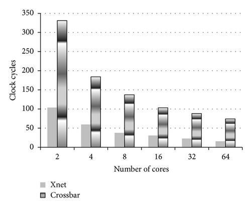
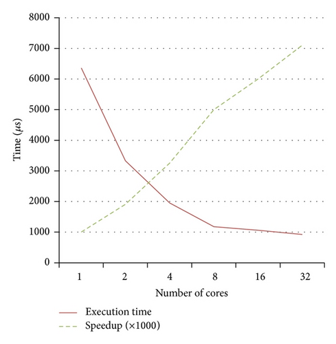
( 2) Spatial Laplacian Filter. We consider a 2D filter such as Laplacian filter, which smooths a given image (of size 800 × 480 pixels) by convolving it with a Laplacian kernel (3 × 3 kernel [9]). The parallel algorithm implemented in this work has been proposed in [18]. Such application can be performed in parallel, so that multiple pixels can be processed at a time. Each core reads an amount of pixels (depending of the image size) from an external SDRAM memory and stores them in vectors. Then, it multiplies the vector elements by the filter kernel coefficients. After that, all resultant elements are added and divided for scaling. As a result, each core simultaneously produces a convolution of n pixels, where n is the number of cores integrated in the system. In this algorithm, we need to integrate the global router to assure data transfers from SDRAM to data memories of the processors. The controller is so responsible of controlling and configuring the network. The execution time results and speedup values are shown in Figure 6 varying the number of cores. Figure 6 clearly shows that the speedup exponentially increases while increasing the number of cores. It shows a good scalability since doubling the number of cores provides an average speedup of 1.6. We deduce that the multicore system is efficient to compute image processing applications. For example, we reach a speedup 5 times over a sequential execution when integrating 8 PEs, which is quite appreciable. It is also noted that the execution time slightly decreases between 16 and 32 cores due to the time needed to accomplish communications.
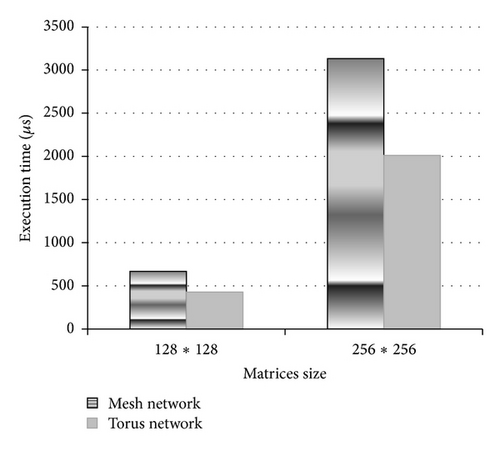
( 3) Matrix-Matrix Multiplication. One of the basic computational kernels in many data parallel codes is the multiplication of two matrices (C = A × B). Matrix multiplication is considered an important kernel in computational linear algebra. It is a very compute-intensive task, but also rich in computational parallelism, and hence well suited for parallel computation [19]. In this work, the tested multicore configuration integrates 64 PEs. We study the influence of the interconnection network topology on the application performance. The PEs are arranged in 8 × 8 grid. To perform multiplication, all-to-all row and column broadcasts are performed by the PEs. The following code for PE(i, j) is executed by all PEs simultaneously, in a 64-core configuration. In this case, matrices A and B, of size 128 × 128, are partitioned into submatrices A(i, j) and B(i, j) of size 16 × 16.
/* East and West data transfer */
For k = 1 to 7 do
Send A(i,j) to PE(i,(j+k) mod 8)
/* North and South data transfer */
For k = 1 to 7 do
Send B(i,j) to PE((i+k) mod 8,j)
/* Local multiplication of submatrices */
For k = 0 to 7 do
C(i,j) = C(i,j) + A(i,k) x B(k,j).
The obtained time results are depicted in Figure 7 with differently sized matrices. Figure 7 demonstrates that the used network influences the total execution time. In our case, it was easy to test different topologies thanks to the implemented mode instruction. From the SW level, the programmer can choose the interconnection network topology they want to use. The results show that the Torus network is the most appropriate neighbourhood network for the matrix-matrix multiplication.
To further evaluate the performance of the implemented multicore configurations, we measure the communication-to-computation ratio (CCR) for the three tested benchmarks based on a 32-core configuration. Table 5 depicts the obtained results. It is clearly shown that the measured communication-to-computation ratio is small, which indicates that the number of processing cycles exceeds the number of communication cycles. This allows having a good speedup.
| Benchmark | CCR |
|---|---|
| FIR filter | 0.51 |
| M-M multiplication | 0.47 |
| Spatial Laplacian filter | 0.32 |
Table 6 shows the parallel efficiency for the tested benchmarks depending on the number of PEs. The parallel efficiency decreases as the number of cores increases. We notice that the efficiency drops down to 12%, when executing the FIR filter with 64 cores. In this case, the additional cores do not deliver additional performance due to the needed extra communications. Through these results, we can choose the best number of cores to parallelize a given application.
| Number of PEs | Efficiency (%) | ||
|---|---|---|---|
| FIR filter | Laplacian filter | M-M multiplication | |
| (with Xnet) | (matrices of size 128 * 128) | ||
| 2 | 84 | 95 | 97 |
| 4 | 74 | 81 | 88 |
| 8 | 59 | 62 | 81 |
| 16 | 36 | 37 | 75 |
| 32 | 24 | 22 | 66 |
| 64 | 18 | — | 59 |
5. Multicore Architectures and Performance Analysis
5.1. Related Work
Several on-chip multicore platforms have been proposed [20]. Different multiprocessor architectures with the NIOS II softcore were also presented in [21]. These platforms are designed to raise the efficiency in terms of GOPS per Watt. In this work, a particular attention is given to architectures working in SIMD/SPMD fashion and prototyped on FPGA devices.
One of the famous high performance architectures is the GPGPU. The Fermi processor is an example [22]. It is composed of 512 cores. However, these architectures present some limits in terms of the access memory bottleneck since all cores share the same memory and the high power consumption making them not suitable in the embedded system field.
In [23], the authors present a parameterizable coarse-grained reconfigurable architecture. Different interconnect topologies can be reconfigured, and static as well as dynamic parameters are described. This work mainly concentrates on providing a dynamic reconfigurable network by developing a generic interconnect wrapper module. The PEs used in the design have limited instruction memory and can only execute specific instructions needed in digital signal processing.
In [24], the authors present massively parallel programmable accelerators. The authors propose a resource-aware parallel computing paradigm, called invasive computing, where an application can dynamically use resources. They show that the invasive computing allows reducing energy consumption by dynamically powering off the idle regions at a given time.
A many-core computing accelerator for embedded SoCs, called Platform 2012, is presented in [25]. It is based on multiple processor clusters and works in MIMD fashion. One cluster can hold a number of PEs (STxP70-V4 processor) varying from 1 to 16. P2012 is a Globally Asynchronous Locally Synchronous (GALS) fabric of clusters connected through an asynchronous global NoC.
The Cell Broadband Engine Architecture (CBEA) [18] is a multicore system, which integrates a PowerPC PE and 8 Synergistic PEs dedicated to compute intensive applications. It has been shown to be significantly faster than existing CPUs for many applications.
Many modern commercial microprocessors also have SIMD capability, which has become an integral part of the Instruction Set Architecture (ISA). Design methods include combining a SIMD functional unit with a processor or exploiting the SIMD instructions extension [26] present in softcores to run data-parallel applications. SIMD extensions are used, for example, in ARMs Media Extensions [27] and PowerPCs AltiVec [28]. The SIMD-style media ISA extensions are presented in most high-performance general-purpose processors (e.g., Intels SSE1/SSE2, Suns VIS, HPs MAX, Compaqs MVI, and MIPs MDMX). Their drawback is due to their data access overhead for instructions, which becomes an obstacle to the performance enhancement.
In [29], the authors present heterogeneous multicore architectures with CPU and SIMD 1-dimensional PE array (SIMD-1D) and MIMD 2-dimensional PE array (MIMD-2D) accelerators. A custom hardware address generation unit (AGU) is used to generate preprogrammed addressing patterns in smaller number of clock cycles compared to the ALU-based address generation. The SIMD-1D accelerator has 8 PEs and a 16 bit × 256 16-bank shared memory connected through a crossbar interconnection network. Through a matrix-matrix multiplication benchmark, the authors demonstrate that the proposed SIMD-1D architecture is 15 times power-efficient than GPU for the fixed-point calculations.
Another FPGA-based massively parallel SIMD processor is presented in [30]. The architecture integrates 95 simple processors and memory on a single FPGA chip. The authors show that their proposed architecture can be used to efficiently implement an RC4 key search engine. An application-specific multicore architecture designed to perform a simple cipher algorithm is presented in [31]. The architecture consists of four main modules: the sequential processor that is responsible for the interpretation and execution of a user-defined program, the queuing module that is responsible for scheduling tasks received from the sequential processor, four parallel processors that are idle until they get tasks from the queuing module, and the parallel memory that holds the data and key for processing and allows for concurrent access from all parallel processors. There is also a monitoring module which interprets user-control signals and sends back their results via a specified output. The architecture can integrate more parallel cores; however this can be done manually and so requires long design time.
These different platforms are summarized in Table 7.
| Reference | Author | Year | CPU type | # cores | Network | Memory architecture | Tested application |
|---|---|---|---|---|---|---|---|
| [30] | Li et al. | 2003 | FPGA-based massively parallel SIMD processor | 95 simple processors | — | — | RC4 key search engine |
| [23] | Kissler et al. | 2006 | Parameterizable coarse-grained reconfigurable architecture | Parametric number of weakly programmable PEs | Different interconnect topologies (Torus, 4D hypercube, etc.) | — | — |
| [18] | Ruchandani and Rawat | 2008 | CBEA | 8 PEs + PowerPC | Elementary interconnect bus (EIB) |
|
Spatial domain filter |
| [22] | Wittenbrink et al. | 2011 | Fermi proc (GPGPU) | 512 | — | Shared memory | Gaming and high-performance computing |
| [25] | Melpignano et al. | 2012 | P2012 (MIMD) | Multiple clusters; one cluster can have from 1 to 16 PEs | Asynchronous global NoC | Shared memory | Extraction and tracking algorithms |
| [29] | Waidyasooriya et al. | 2012 | Heterogeneous multicore architecture | SIMD-1D 8 PE array and MIMD-2D PE array accelerators | Crossbar | Shared memory | M-M multiplication |
| [31] | Wjcik and Dlugopolski | 2013 | Application-specific multicore architecture | 4 parallel processors | — | Shared parallel memory | Cipher algorithm |
| [24] | Lari et al. | 2014 | Massively parallel programmable accelerator | Parametric number of tightly coupled PEs | Circuit-switched Mesh-like interconnect | Multiple buffer banks | Loop computations |
| Proposed work | 2014 | FPGA-based multicore SoC | Parametric number of cores | Crossbar | Local private memory |
|
|
5.2. Performance Analysis
The multicore architecture, discussed in this paper, is suitable for data-intensive computations. Comparing with embedded general-purpose graphics processing units, such architectures have both huge number of processing units; however, there exist also some differences. GPUs used in multiprocessor systems-on-a-chip have direct access to the main memory, shared with the processor cores. In GPUs, there is no neighbouring communication between the cores. Thus, exchanging data is made via the shared memory. In contrast, the PEs in the proposed multicore SoC can communicate with each other and also other components via two networks. GPUs are mainly dedicated to massively regular data-parallel algorithms. However, the proposed multicore architecture can handle both regular and irregular data parallel algorithms thanks to its communication features. To validate this reasoning, our multicore SoC and a commercial embedded GPU are evaluated for selected algorithms (FIR filter and matrix-matrix multiplication). A Samsung Exynos 5420 Arndale Octa Board is used. It features a dual-core ARM Cortex-A15 that runs at 1.7 GHz and an ARM Mali T-604 GPU operating at 533 MHz [32]. The GPU has a theoretic peak performance of 68.22 GOPS. For the comparison, a 16-core configuration (the PEs are connected via a Xnet network) was considered. The multicore architecture operated at 337 MHz. The considered architecture has a peak performance of 10.78 GOPS. The performance comparison is illustrated in Table 8. Execution time measures and the achieved fraction of the peak performance are highlighted.
| Application | GPU | 16-core configuration | ||
|---|---|---|---|---|
| Exec. time | % peak perf. | Exec. time | % peak perf. | |
|
655 μs | 18.8% |
|
|
|
2 634 μs | 18.7% |
|
|
Table 8 shows that our proposed multicore system achieves better speedup than the GPU (29% faster for the FIR filter and 23% faster for the matrix-matrix multiplication). Our system is also more efficient since it achieves a better fraction of the peak performance than the GPU. This proves the well resource utilization in the multicore on-chip implementation. The aforementioned results demonstrate the performance of the proposed architecture. We think that our system can be coupled with GPU to form a high-performance multiprocessor system.
Tanabe et al. [33] propose an FPGA-based SIMD processor. The proposed architecture is based on SuperH processor that was modified to include more numbers of computation units and then performs SIMD processing. A JPEG case study was presented; however no idea about programming was given. The achieved clock frequency of the SIMD processor is too low (55 MHz) while many softcores run faster these days. Table 9 compares between our multi-softcore architecture and the architecture described in [33] composed of one control unit and a number of computation units (CU) in terms of power consumption and frequency. As illustrated, our system achieves good results since it presents a higher frequency and a lower power consumption compared to the SIMD processor. The replication design methodology makes the design of a multi-softcore architecture easier and can integrate a parametric number of PEs compared to the used dedicated implementation [33] that makes adding more computational units to the architecture a heavy task.
| Proposed multi-softcore SoC | Fmax | Power (mW) | [33] | Fmax | Power (mW) |
|---|---|---|---|---|---|
| 4 PEs | 412 | 756 | 4 CUs | 56 | 1 149 |
| 8 PEs | 382 | 834 | 8 CUs | 55 | 1 233 |
| 16 PEs | 337 | 1 151 | 16 CUs | 52 | 1 385 |
Compared to the multicore architecture described in [31] which is application specific, our proposed architecture is parametric and scalable and can satisfy a wide range of data-intensive processing applications. In addition, our system integrates two types of flexible communication networks that can efficiently handle communication schemes present in many applications. In terms of performance, our multicore architecture can reach a speedup of 1.9 with two cores and 3.2 with four cores. In comparison, the achieved results presented in [31] show a speedup reaching 1.85 with two cores and 2.92 with four cores active.
The preceding performance comparison confirms the promising advantages and performance of the proposed FPGA-based multicore architecture. This paper proves that an FPGA-based multicore design built with softcores is powerful to compute data-intensive processing. The presented architecture is easy to design, configurable, flexible, and scalable. Thus, it can be tailored to different data-parallel applications.
6. Conclusion
In this paper, we have presented a softcore-based multicore implementation on FPGA device. The proposed architecture is parametric and scalable, which can be tailored according to application requirements such as performance and area cost. Such a programmable architecture is well suited for data-intensive applications from the areas of signal, image, and video processing applications. Through experimental results, we have demonstrated better performance gains of our system in comparison to state-of-the-art embedded architectures. The presented architecture provides a great deal of performance as well as flexibility.
Future work will focus on studying the energy efficiency of the presented system, as power consumption is considered the hardest challenge for FPGAs [34]. We want to explore the usage of custom accelerators in the proposed architecture. We also envision studying a possible dynamic exploitation of the available level of parallelism in the multicore system based on the application requirements.
Conflict of Interests
The authors declare that there is no conflict of interests regarding the publication of this paper.


