Characterization and Modeling of CdS/CdTe Heterojunction Thin-Film Solar Cell for High Efficiency Performance
Abstract
Device simulation is used to investigate the current-voltage efficiency performance in CdTe/CdS photovoltaic solar cell. The role of several limiting factors such as back contact Schottky barrier and its relationship to the doping density and layer thickness is examined. The role of surface recombination velocity at back contact interface and extended CdTe layer is included. The base CdS/CdTe experimental device used in this study shows an efficiency of 16-17%. Simulation analysis is used to optimize the experimental base device under AM1.5 solar spectrum. Results obtained indicate that higher performance efficiency may be achieved by adding and optimizing an extended CdTe electron reflector layer at the back Schottky contact. In the optimization of the CdS/CdTe cell an extended electron reflector region with a barrier height of 0.1 eV and a doping density of 7 × 1018 cm−3 with an optimum thickness of 100 nm results in best cell efficiency performance of 19.83% compared with the experimental data.
1. Introduction
Among the thin-film solar cells, the commonly used are amorphous silicon, CuInGaSe2, and CdTe. At the present, the amorphous silicon solar cells have the largest market share in the world with less a fraction of one percent to CuInGaSe2 and about a few percen to CdTe cells. The benefit of using CdTe is for being a direct bandgap material with high absorption (in relationship with silicon) and the ease of device processing, can be deposited on glass in thin film typically a few micrometers and at low temperature [1–7].
Large-area CdTe photovoltaic panels can be economically fabricated, potentially making the CdTe thin-film solar cell a leading alternative energy source. However, the recorded experimental CdTe efficiency of 16.5% is much less than its theoretical maximum efficiency of 29%, where the open-circuit voltage of 0.845 V is well below what is expected for its bandgap of 1.42 eV [8–10]. The experimental measurement obtained by others is used as a benchmark for the optimization of the CdS/CdTe cell and for the development of the strategies to improve the efficiency referred to here as base device [11].
An important issue related to the limiting performance of the CdTe cells is the back contact. Experimental works show that the CdTe cells at back contact form Schottky barrier thus degrading the cell efficiency and performance [12–18]. Other limiting factors in performance of CdTe cells are related to the unavailability of the physical material properties which is at incubator status when compared with the mature technology of the silicon and silicon electronics [19–26].
The modeling approach adopted in this paper allows us to examine device design and the role of material parameters in the performance and efficiency of the cell. Device simulation is used to predict the characteristics of CdS/CdTe heterojunction solar cells by identifying material parameters essential for improving the cell performance. Issues related to doping concentration, surface recombination, and extended region back contact Schottky barrier are investigated.
The modeling work on CdTe structures is based on simulation program, AFORS-HET [27–29]. The software program has been used in the development and design of several solar cells in the past. The device modeling solves relatively large number of nonlinear and tightly coupled partial differential diffusion equations and uses several position-dependent material and transport parameters that make it robust. The device equations are solved over a set of mesh geometry. In addition, for solar cell structures the model includes optical absorption and a broad spectrum of light input that can be supplied to properly simulate the characteristics of a solar cell. In the next sections we will show in detail that the program works well for CdTe/CdS photovoltaic devices.
2. Device Design and Analysis
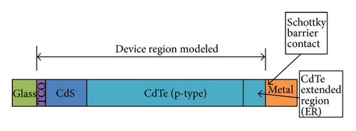
The schematic of a CdTe thin-film solar cell used in the simulation with TCO/CdS(n-type)/CdTe(p-type)/metal structure is shown in Figure 1.
In this design, the carrier density of CdTe p-type layer is 7 × 1016 cm−3 (similar to the experimental data) with heavy doped CdS n-layer of 1 × 1018 cm−3. The CdTe is a direct bandgap semiconductor with a large absorption coefficient. Because of this important optical property, very thin CdTe layers can be used for photovoltaic applications. For the simulation, we have used a film thickness of 2 μm as in the typical CdTe solar cell manufacturing [30–35]. Table 1 shows the characteristics of ZnO-TCO layer. A 500 nm thick TCO layer with an n-type doping density of 1 × 1018 cm−3 is assumed. For this structure, the depletion region is formed in CdTe absorption layer. That is, a 2 μm CdTe cell and a doping density of 7 × 1016 cm−3 become fully depleted. It is desirable to have photons absorbed in this region where light induced carriers can be collected with the assistance of the built-in electric field. Similarly, at a wavelength of 600 nm, a 2 μm of CdTe layer will absorb more than 99% of incident light, making CdTe a suitable candidate for absorption material for photovoltaic applications.
| Parameter | CdTe | CdS | ZnO (TCO) |
|---|---|---|---|
| Eg (eV) | 1.42 | 2.53 | 3.4 |
| Electron Affinity (eV) | 4.28 | 4.5 | 4.5 |
| μn (cm2/v·s) | 500 | 340 | 100 |
| μp (cm2/v·s) | 60 | 50 | 25 |
| Relative Dielectric Constant | 10.9 | 8.9 | 9 |
| Density of state for electron (cm−3) | 7.8 × 10¹⁷ | 2.22 × 10¹⁸ | 2.22 × 10¹⁸ |
| Density of state for hole (cm−3) | 1.8 × 10¹⁹ | 1.8 × 10¹⁹ | 1.9 × 10¹⁹ |
| Index of Refraction | 2.76 | 2.51 | 2.006 |
| Doping Density (cm−3) | 7 × 10¹⁶–7 × 10¹⁸ p-type | 1 × 10¹⁸ n-type | 1 × 10¹⁸ n-type |
| ZnO/CdS ΔEc (eV) | 0.0 | ||
| ZnO/CdS ΔEv (eV) | 0.87 | ||
| CdS/CdTe ΔEc (eV) | 0.22 | ||
| CdS/CdTe ΔEv (eV) | 0.89 |
Other device parameters are CdS layer with a thickness of a 40 nm and ZnO transparent conductive oxide (TCO) layer with a thickness of 0.5 μm. The TCO layer with a bandgap energy of about 3.4 eV is used to minimize the optical loss where at this high sun energy TCO prevents less blue light from reaching CdTe for a thick CdS layer.
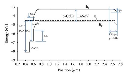
The layer of CdTe is assumed to have an electron affinity of 4.28 eV and a bandgap of 1.42 eV. In order to create an ohmic contact, a metal with a work function greater than or equal to 5.7 eV (the sum of electron affinity and bandgap) is required. As a result most metal contacts applied to p-type CdTe such as copper with work function of 4.6 eV, nickel with 5.1 eV, or titanium with 4.3 eV create nonohmic Schottky type barrier contact which limits the overall performance efficiency of the CdTe cell [36, 37]. As shown in Figure 4, the incorporation of an electron reflector (ER) at back contact is proposed by other investigators to improve the open-circuit voltage of solar cells, and to improve the efficiency of CdTe thin film [3, 8, 10–12].
In a heavily doped p-type metal back contact, the majority of hole carriers are transported by the tunneling in a thin junction of approximately a few nanometer. The optimization and development of the back contact is a limiting factor addressed in this paper and crucial for achieving a high efficiency cell.
3. Experimental Data
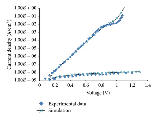
A device structure similar to one described in reference [11] is considered. As shown in Figure 3, the measured room temperature dark current-voltage characteristics of the ZnO/CdTe/CdS cell are compared with the simulation result. Data of Table 1 is used in the simulation analysis [10–12]. In addition, a carrier lifetime of 5 × 10⁻¹⁰ s is used. In this model it is assumed that the recombination center is located at the center of the bandgap energy resulting in modeling the recombination of carriers with a constant lifetime. The analysis shows that there is an extended portion of the current-voltage curve (less than 0.8 V) that can be modeled with an ideality factor of about 2 where recombination in the space charge region is dominating. In this comparison the goal was not to obtain a best fit but rather to develop a realistic device structure to study the effect of back Schottky contact on the performance of the cell. Here, a structure with the p-type CdTe doping of 7 × 1016 cm−3 and a thickness of 2 μm becomes the base device for our optimization. This device shows a maximum short-circuit current density of about 28.4 mA/cm2 which will be used throughout this study.
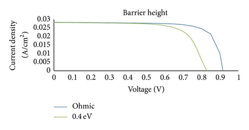
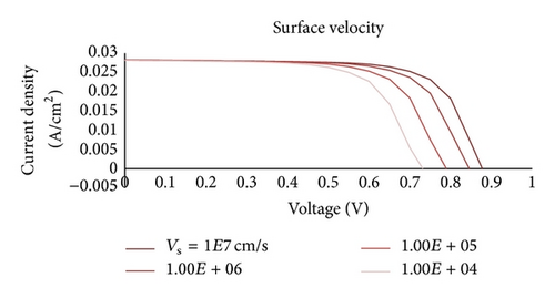
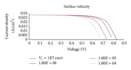
Simulation results for a base device show that by reducing the barrier height φe from 0.4 to 0.1 eV a higher open-circuit voltage may be obtained while the short-circuit current remains virtually constant. These results are summarized in Table 2. In addition a higher overall cell efficiency can be achieved with the reduced φe. An optimized device shows a φe of about 0.1 eV. The base device has an efficiency of about 16.38% similar to the experimental data. Moreover, the base device shows an efficiency of about 17.46% assuming an ohmic contact with an infinite surface recombination velocity of 1 × 107 cm/s (Figure 5). We chose the simulation data and analysis mostly around a device with a barrier height of 0.3–0.4 eV as this number is more closely related to a realistic CdTe device structure with back Schottky contact [12, 15–18, 31].
| Barrier height (eV) | Voc (mV) | Jsc (mA/cm2) | FF (%) | Efficiency (%) |
|---|---|---|---|---|
| 0.1 | 916 | 28.36 | 75.91 | 19.72 |
| 0.2 | 916 | 28.35 | 75.76 | 19.67 |
| 0.4 | 830 | 28.23 | 69.8 | 16.36 |
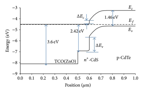
In the absence of an electron reflector or extended region, the band bending of the back surface results in surface recombination degrading the device performance (Figure 2). The surface recombination velocity is a function not only of the material quality and the device but also of the doping level. The exact value of surface recombination velocity is frequently not known but typically extracted from the measured data of a given device. The back surface recombination is considered a major limitation factor on a cell’s performance in thin devices. The built-in field at the back surface can drive the carriers away from the back surface, thereby affecting recombination rate. In addition, the electric field at back surface may also increase the probability for electron-hole generation near the back contact. A higher velocity is desirable which improves the contact condition toward an ohmic status thus reducing the loss of carriers. As shown in Figure 6, simulation results show that surface recombination at the back contact significantly reduces the open-circuit voltage.
4. Electron Reflector Layer Thickness
For the optimization of the device an offset to the CdTe, absorption layer is considered by adding a CdTe layer as an electron-reflector-extended region (ER), (Figure 4). In addition to CdTe, other materials such as CdZnTe, CdMnTe, and CdMgTe may be employed in creating an ER layer [10, 14, 15, 17, 29, 36].
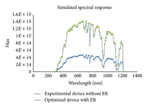
A thin-layer electron reflector causes the depletion region of the Schottky barrier contact to be narrow where majority of hole carriers can tunnel through minimizing the loss. The simulated spectral density of the CdTe cell with and without the introduction of the ER is shown in Figure 7. As shown in this figure an ER layer may also add an additional absorption layer to the structure thus increasing the spectral response by increasing photogenerated carriers. The thickness of ER layer used in the simulation of spectral response is 100 nm, and the ER doping density is assumed to be 7 × 1016 cm−3.
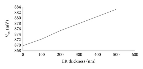
The tradeoff between the open-circuit voltage and short-circuit current when ER is included is shown in the simulated results of Table 3. As shown in Figure 8, the short-circuit current remain relatively constant with the ER layer thickness while the open-circuit voltage increases. In this example the thickness of extended region ranges from 50 nm to 500 nm where the doping density and the barrier height are kept constant at 7 × 1016 cm−3 and 0.3 eV, respectively. As indicated earlier in the discussions, the simulation data and analysis are chosen mostly around a device structure with a barrier height of 0.3–0.4 eV as this number is closely related to a realistic CdTe device with Schottky barrier contact [12, 15–18, 31].
| ER thickness (nm) | Voc (mV) | Jsc (mA/cm2) | FF (%) | Efficiency (%) |
|---|---|---|---|---|
| 0 | 869.9 | 28.27 | 71.0 | 17.46 |
| 100 | 872.3 | 28.3 | 70.89 | 17.50 |
| 200 | 875.4 | 28.31 | 70.65 | 17.51 |
| 500 | 883.2 | 28.33 | 70.06 | 17.53 |
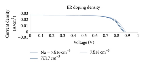
Normally the extended layer is heavily doped to minimize the negative effect of the Schottky barrier. Table 4 summarizes the simulated results for an example where the doping density of ER layer varied from 7 × 1016 cm−3 to 7 × 1018 cm−3. The thickness of ER layer and the barrier height are kept constant at 100 nm and 0.3 eV, respectively. Further simulation analysis and results show that the best performance efficiency of about 19.83% may be obtained with an ER layer doping of 7 × 1018 cm−3 and an ER thickness of 100 nm at a barrier height of 0.1 eV.
| ER with different doping (cm−3) | Voc (mV) | Jsc (mA/cm2) | FF (%) | Efficiency (%) |
|---|---|---|---|---|
| 7 × 10¹⁶ | 872.3 | 28.3 | 70.89 | 17.50 |
| 7 × 10¹⁷ | 877.7 | 28.29 | 71.26 | 17.70 |
| 7 × 10¹⁸ | 891 | 28.32 | 71.21 | 17.97 |
5. Conclusion
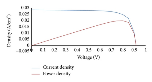
The analysis obtained shows that in the optimization of the cell combining the two mechanisms of heavy doping and extended region are the key parameters to achieve a better cell design. Our results show that in addition to a low surface recombination velocity of 1000 cm/s at back contact and a barrier height of 0.1 eV, an ER layer of 100 nm with a doping density of 7 × 1018 cm−3 is also required to produce the best cell efficiency performance of 19.83% summarized in Table 5. The photocurrent characteristics of the optimized cell with Voc of 917.6 mV, Jsc of 28.45 mA/cm2, and an efficiency of 19.83% are shown in Figure 10. In the summary a number of different design parameters are used to optimize CdS/CdTe heterojunction thin-film cell (Figure 9). Simulation results show for an optimum efficiency performance a doping density of 7 × 1018 cm−3 and ER layer thickness of 100 nm are needed, as summarized in Table 5.
| ER different thickness (nm) | Voc (mV) | Jsc (mA/cm2) | FF (%) | Efficiency (%) |
|---|---|---|---|---|
| 100 | 917.6 | 28.45 | 75.99 | 19.83 |
