Photovoltaic Power System with an Interleaving Boost Converter for Battery Charger Applications
Abstract
This paper proposes a photovoltaic (PV) power system for battery charger applications. The charger uses an interleaving boost converter with a single-capacitor turn-off snubber to reduce voltage stresses of active switches at turn-off transition. Therefore, active switches of the charger can be operated with zero-voltage transition (ZVT) to decrease switching losses and increase conversion efficiency. In order to draw the maximum power from PV arrays and obtain the optimal power control of the battery charger, a perturbation-and-observation method and microchip are incorporated to implement maximum power point tracking (MPPT) algorithm and power management. Finally, a prototype battery charger is built and implemented. Experimental results have verified the performance and feasibility of the proposed PV power system for battery charger applications.
1. Introduction
Due to the continuous growth of the global energy demand for developing industry, it increases society awareness of environmental impacts from the widespread utilization of fossil fuels, leading to the exploration of renewable energy sources, such as PV arrays, wind energy, and so on. One of these sources is PV arrays energy, which is clean, quiet, and maintenance-free. However, due to the instability and intermittent characteristics of PV arrays, it cannot provide a constant or stable power output. Thus, a power converter (dc/dc converter or dc/ac converter) and MPPT algorithm are required to regulate its output power.
Several MPPT algorithms have been proposed [1–10]. Some of the popular MPPT algorithms use perturbation-and-observation method [1–3], incremental conductance method [4], constant voltage method [5, 6], β method [7], system oscillation method [8, 9], and ripple correlation method [10]. The perturbation-and-observation method requires the measurement of only a few parameters, thus it facilitates an MPPT control. As a result, it is often applied to the PV arrays for enhancing power capacity.
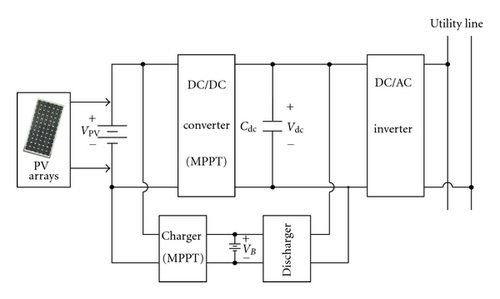
A typical PV power system is shown in Figure 1. The PV arrays usually need a battery charger to increase its utility rate. The research of this paper is only focused on PV arrays for battery charger applications. For charger design, many charging methods have been developed, such as the constant trickle current (CTC), constant current (CC), constant voltage (CV), hybrid CC/CV [11], and reflex charging methods [12–15]. The CTC method has a disadvantage that it has a longer charging time, the CC and CV are the simplest methods to battery charger, but both of them result in the situations of undercharge and overcharge. The hybrid CC/CV method can improve charging efficiency and charging time, but it has a disadvantage of difficult control. To reduce the charging time of the batteries, the reflex charging method is adopted in this paper. The method consists of a high positive pulse-charging current followed by a high current, short time negative pulse-discharging current, and a rest period. A high positive pulse-charging current can reduce the charging time and a negative pulse-discharging current is to reduce internal cell pressure and temperature of batteries. A rest period can provide the batteries with a reflex time in charging process.
The basic switching power converters have six circuit structures, such as buck, boost, buck-boost, Cuk, Sepic, and Zeta converters. In order to obtain continuous input current for battery charger, the basic boost converter is widely used. However, it is operated under high switching frequencies resulting in high switching losses, noises, and component stresses. These drawbacks reduce power seriously and deteriorate in the performances of the basic boost converter. In order to alleviate the problems described previously, soft-switching technologies are introduced into the basic boost converter to reduce switching losses. Soft-switching technologies can be classified as passive and active soft-switching technologies. The passive technologies use only passive components to perform soft-switching operation [16–18]. The active technologies add one or more active switches along with other passive components to the basic switching power converters to perform soft-switching operation [19, 20]. For cost considerations, the proposed battery charger with passive soft-switching technologies is more attractive at low power level applications.
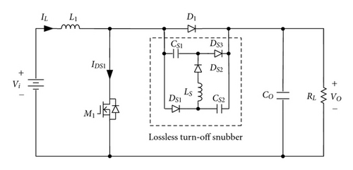
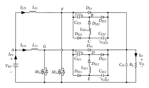
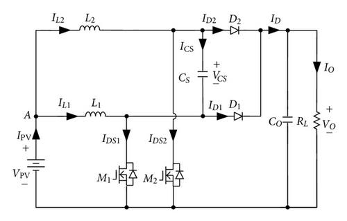
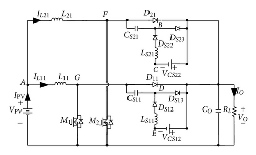
A basic boost converter with a passive lossless turn-off snubber for battery charger applications is usually adopted, as shown in Figure 2 [18], because it has a simple structure. However, the basic boost converter has a disadvantage that its output ripple current will swing over a wide range resulting in a low battery life. In order to reduce output ripple current and increase power level, two sets of boost converters are incorporated with an interleaving fashion, as shown in Figure 3 [21]. Although interleaving boost converter with two sets of passive soft-switching circuits can also achieve soft-switching features, their component counts and cost are increased significantly. To overcome the previously discussed drawbacks, an interleaved boost converter with a single-capacitor turn-off snubber for battery charger applications is proposed, as shown in Figure 4. The proposed battery charger requires only a resonant capacitor CS which is associated with inductors L1 and L2 to reduce switching losses of active switches.
2. Control Algorithm of the Proposed Charger
In order to achieve an optimal power control of battery charger, an MPPT algorithm and a power management unit are needed. These control algorithms are described as follows.
2.1. Topology of Battery Charger
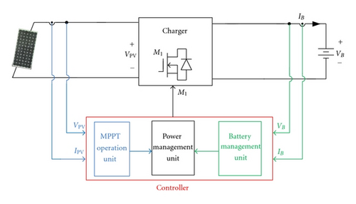
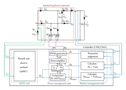
The proposed charger includes an interleaving boost converter and a controller, as shown in Figure 5. Moreover, the controller adopts microchip to implement MPPT of PV arrays and battery charging management. Therefore, the controller of the proposed battery charger can be divided into three units. They are MPPT operation, battery management, and power management units. The MPPT operation unit can implement the MPPT of PV arrays. The charging algorithm of battery charger is controlled with reflex charging method by battery management unit to reduce the charging time. In order to achieve the best energy utilization of the PV arrays, an MPPT with perturbation-and-observation method is integrated into an MPPT operation unit. Since the MPPT and charging algorithm must be associated to implement optimal control of battery charger, the power management unit is needed. To achieve optimal stability and safety for the proposed battery charger, the functions of under-voltage, over-current, and over-temperature protection circuits are required. All of the protection signals are also realized on a microchip.
2.2. MPPT Algorithm
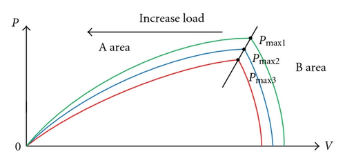
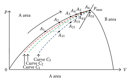
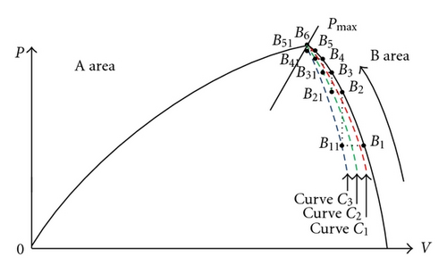
Output characteristic variations of PV array depend on climatic conditions, such as temperature of PV arrays and insolation of sun. Its P-V curves at different insolation of the sun are shown in Figure 6. From Figure 6, it can be seen that each insolation level has a maximum power Pmax , where Pmax 1 is the maximum power at the largest insolation of sun while Pmax 3 is the one at the least insolation of sun. Three maximum power points Pmax 1 ~ Pmax 3 can be connected by a straight line. Operational area on the right hand side of the straight line is defined as B area, while the one on the left hand side is defined as A area. Since output load connected in PV arrays increases, output voltage of PV arrays decreases. Therefore, when working point of PV arrays locates in A area, output load must decrease to make the working point to approach the maximum power point of PV arrays. On the other hand, when working point of PV arrays places on B area, output load must increase. Their operation conditions are shown in Figure 7. Figure 7(a) shows the working point located on A area, while Figure 7(b) illustrates the one located on B area. When working point locates on A area, the working point is changed from A1 to maximum power point Pmax at point A6 through A2, A3, A4, and A5, as shown in Figure 7(a). When working point locates on B area, the working point is changed from B1 to maximum power point Pmax at point B6 through B2, B3, B4, and B5, as shown in Figure 7(b). According to different operational area to increase or decrease output load, working point of PV arrays can be shifted to MPP.
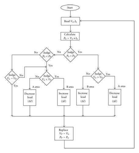
In order to extract maximum power of PV arrays, a simple perturbation-and-observation method is adopted. Its flow chart is shown in Figure 8. In the MPPT flow chart, Vn and In are, respectively, new voltage and current of PV arrays, VP and PP separately represent its old voltage and power value, and Pn( = Vn In) is the new power value of PV arrays. According to flow chart of MPPT using perturbation- and observation-method, the first step is to read new voltage Vn and current In of PV arrays, and then to calculate new PV power Pn. The next step is to judge the relationship of Pn and PP. According to the relationship of Pn and PP and procedures of MPPT flow chart, the procedure enters to judge the relationship of Vn and VP. When the relationship of Vn and VP is decided, operational area of working point can be specified. According to control algorithm of MPPT, when the working point of PV arrays is located in A area, power system connected in PV arrays to supply load power must decrease output power to close the distance between working point and MPP of PV arrays. On the other hand, when the operating point is located in B area, PV power energy must be increased to approach maximum power point of PV arrays. Finally, the procedure of MPPT flow chart is returned to the first step to judge next maximum power point of PV arrays.
2.3. Power Management
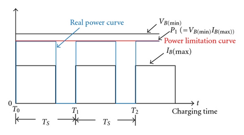
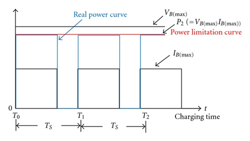
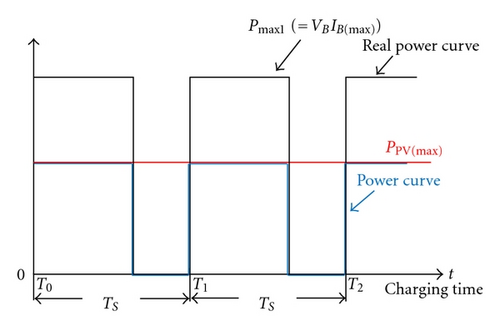
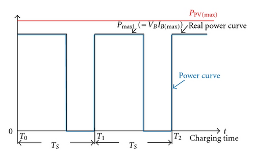
The proposed charger is with a reflex charging method to reduce charging time, since the charging voltage and current of batteries must be limited for protecting battery life. The conceptual waveforms of charging current and voltage of battery charger with a reflex charging method are shown in Figure 9. Figure 9(a) shows reflex charging waveforms of battery charger under minimum battery voltage VB(min ), its VB(min ) is expressed as undercharge condition of battery voltage. Figure 9(b) shows reflex charging waveforms of battery charger under maximum battery voltage VB(max ), its VB(max ) is expressed as overcharge condition of battery voltage. According to VB(min ) and IB(max ) or VB(max ) and IB(min ), the power limitation curve of battery charger can be obtained, as shown in Figure 9. When the maximum power PPV(max ) of PV arrays is larger or less than Pmax 1, the power operation point of PV arrays is traced as shown in Figure 10. As mentioned previously, the charging and discharging power of the proposed charger will be limited by power curve to extend battery life.
3. Derivation and Operational Principle of the Proposed Charger
In order to describe the merits of the proposed battery charger, its topology derivation and operational principles are briefly described as follows.
3.1. Derivation of the Proposed Charger
To reduce switching losses, a lossless turn-off snubber is inserted in a basic boost converter as shown in Figure 2. When switch M1 is turned on, capacitors CS1 and CS2 are charged through inductor Ls and diode DS2 in a resonant manner. At the end of the resonant interval, capacitors CS1 and CS2 are charged to VO and are clamped at VO until switch M1 is turned off. When switch M1 is turned off, the charges stored in capacitors CS1 and CS2 are discharged to output load through diodes DS1 and DS3, respectively. Thus, switch M1 is turned off with zero-voltage transition (ZVT). As mentioned previously, although it can achieve the soft-switching feature, its output current ripple is relatively large for high current and low output voltage applications. Therefore, to reduce output current ripple, an interleaving scheme is usually adopted. In the following, the proposed interleaving boost converter with a single-capacitor snubber is derived.
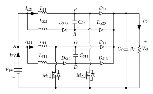
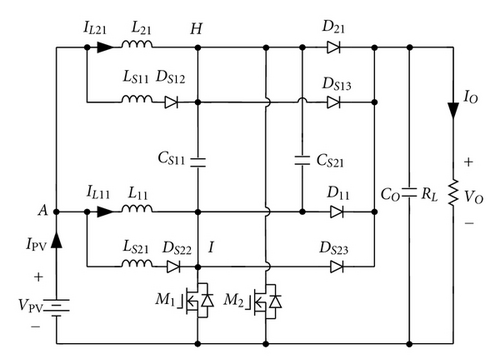
Two lossless turn-off snubbers are used in an interleaving boost converter to reduce switching losses, as shown in Figure 3. To simplify circuit of Figure 3, voltages of capacitors CS12 and CS22 are replaced with dc voltages and , respectively. When voltages of capacitors CS12 and CS22 are replaced with dc voltages, the energies stored in capacitors CS12 and CS22 do not need to discharge their charges. Thus, diodes DS11 and DS21 can be removed, as shown in Figure 11(a). If voltage VCS12 or VCS22 is equal to (VO–VPV), nodes A, C, and E will have the same potential. Thus, they can be merged as node A, as shown in Figure 11(b). Based on the operational principle of an interleaving boost converters and the turn-off snubber, operational states of diode D11 (or D21) is the same as diode DS23 (or DS13) except that the operational duration of the turn-off snubber is operated within resonant mode. Since the duration of resonant mode is much shorter than a period of the proposed converters, nodes F and D (or G and B) can be combined as the same node H (or I), as shown in Figure 11(c). It will not affect its original operational principle. Because inductor currents IL11 and IL21 are unidirectional in the derived converter, inductors L11 and LS21 connected with diode DS22 in series can be combined and replaced by inductor L1. Similarly, inductors L21 and LS11 and diode DS12 can be also merged as inductor L2, as shown in Figure 11(d). In Figure 11(c), since capacitors CS11 and CS21 and diodes D11 and DS23 or D21 and DS13 are, respectively, connected in parallel, they can be, respectively, incorporated as capacitor CS and diode D1 or D2. From Figure 11(d), it can be observed that the derived boost converter requires only a resonant capacitor CS, which is associated with inductors L1 and L2 to function as a lossless turn-off snubber, reducing switching losses and component counts significantly. Therefore, Figure 11(d) is proposed for battery charger applications.

3.2. Operational Principle of the Proposed Charger
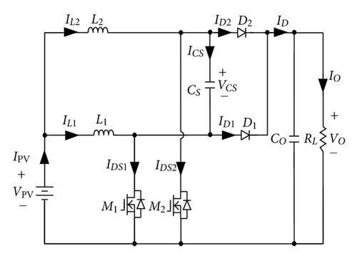
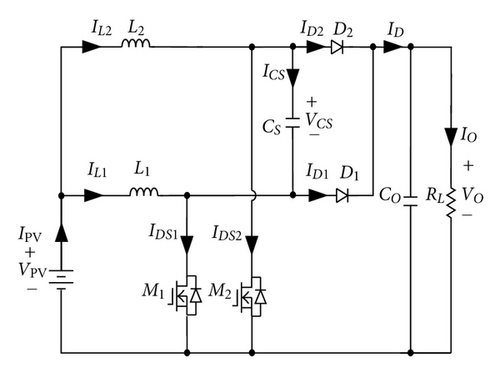
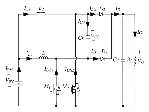
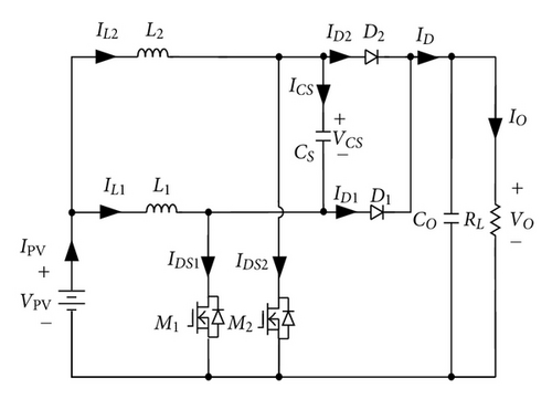
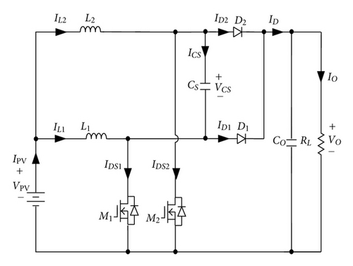
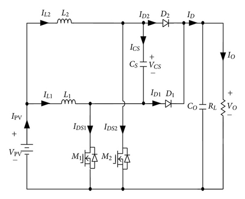
In Figure 4, the proposed battery charger with a single-capacitor turn-off snubber can achieve a ZVT feature for active switches. Operational modes of the proposed charger are divided into ten modes, as illustrated in Figure 12, and their key waveforms are illustrated in Figure 13. In the following, each operational mode is described briefly.
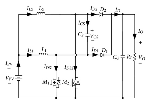

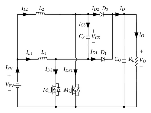

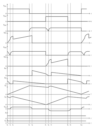
Mode 1 (Figure 12(a); t0 ≤ t < t1). Before t0, diode D2 is in freewheeling, and inductor current IL2 is equal to diode current ID2. At t = t0, switch M1 is turned on. The equivalent circuit at this time interval is shown in Figure 12(a), from which it can be found that switch current is equal to the sum of capacitor current ICS and inductor current IL1. Since the interval of t0 ~ t1 is very short, inductor current IL1 is approximately equal to zero and capacitor voltage VCS is close to zero. Thus, switch current IDS1 is approximately equal to capacitor current ICS. During this time interval, the current ICS is abruptly increased up to inductor current IL2, and ID2 is abruptly decreased down to zero.
Mode 2 (Figure 12(b); t1 ≤ t < t2). At time t1, capacitor current ICS is equal to inductor current IL2, and diode D2 is reversely biased. At this time interval, snubber capacitor CS resonates with inductor L2, and switch current IDS1 is just equal to the sum of resonant inductor current IL2( = ICS) and inductor current IL1. At the same time, capacitor current ICS reaches its maximum value which can be expressed as follows:
Mode 3 (Figure 12(c); t2 ≤ t < t3). When t = t2, capacitor voltage VCS is equal to VO, and diode D2 starts freewheeling through inductor L2. At the same time, switch M1 is still in the on state. The switch current IDS1 is now equal to inductor current IL1 which increases linearly, while inductor current IL2 is decreased linearly.
Mode 4 (Figure 12(d); t3 ≤ t < t4). At time t3, switch Ml is turned off. Because inductor current IL1 must be continuous, capacitor CS starts to discharge for sustaining a continuous inductor current. Thus, switch M1 can be turned off with ZVT.
Mode 5 (Figure 12(e); t4 ≤ t < t5). When time reaches t4, the voltage VCS across capacitor CS is discharged toward zero, and diode D1 starts freewheeling. During this time interval, diodes D1 and D2 are in freewheeling through inductors L1 and L2, respectively.
Mode 6 (Figure 12(f); t5≤ t < t6). At time t5, diode D1 is still in freewheeling, but diode D2 stops freewheeling because inductor current IL2 drops to zero. In this moment, switch M2 is turned on. Inductor current IL1 is equal to the sum of diode current ID1 and capacitor current −ICS. Additionally, because the switch current will flow through the low-impedance path of capacitor CS, diode current ID1 will be dominated by the switch current . That is, within this time duration, capacitor current −ICS is approximately equal to the switch current IDS2. Capacitor current −ICS is abruptly increased up to inductor current IL1, and ID1 is abruptly decreased down to zero.
Mode 7 (Figure 12(g); t6 ≤ t < t7). At time t6, diode D1 is reversely biased, and resonant network formed by capacitor CS and inductor L1 starts resonating. The switch current IDS2 is equal to the sum of inductor current IL1 ( = −ICS) and inductor current IL2 , and capacitor CS is reversely charged.
Mode 8 (Figure 12(h); t7 ≤ t < t8). At t = t7, the capacitor voltage VCS goes down to −VO. The time interval lasts approximately a quarter of the resonant cycle. At the same time, capacitor current −ICS reaches its maximum value, which can be expressed by (1). During this mode, diode D1 starts freewheeling, and inductor current IL2 is increased linearly.
Mode 9 (Figure 12(i); t8 ≤ t < t9). At time t8, switch M2 is turned off. Since the inductor current IL2 must be in smooth transition, capacitor voltage will drop to maintain a continuous inductor current. When t = t9, capacitor voltage VCS drops to zero.
Mode 10 (Figure 12(j); t9 ≤ t < t10). During this time interval, diodes D1 and D2 are in freewheeling through inductors L1 and L2, and their currents ID1 and ID2 are decreased linearly. When switch Ml is turned on again at the end of Mode 10, a new switching cycle will be recycled.
4. Control and Design of the Proposed Charger
In order to achieve optimal control of the proposed charger, the MPPT operation algorithm of PV arrays and reflex charging algorithm of battery must be considered. In the following, control and design of the proposed charger are described.
4.1. Control of the Proposed Charger
The proposed charger consists of an interleaving boost converter and controller. The controller adopts microchip of CY8C27443 made by Cypress Company. Block diagram of the proposed charger is shown in Figure 14. In Figure 14, the CY8C27443 microchip is divided into three units: MPPT, battery management, and power management units. In MPPT unit, the perturbation-and-observation method is adopted to trace maximum power point of PV arrays. The maximum power PP of PV arrays can be decided. Moreover, battery management unit has four input signals (VB, VB(max ), IB, and IB(max )) where VB is the battery voltage, VB(max ) is the set maximum battery voltage, IB is the battery charging current, and IB(max ) is the set maximum battery charging current. According to four input signals, PB( = VB IB) and PB(max )( = VB IB(max )) can be calculated. The PB represents the present charging power of battery, while PB(max ) is the set maximum charging power. In addition, when VB is equal to or greater than VB(max ), protection judgment makes output signal SP from low to high value. The SP is sent to PWM generator for shutdown PWM generator to avoid battery overcharge. In power management unit, a comparator is used to judge relationship of PP and PB(max ). When PP(=PPV(max )) is greater than PB(max ), signal S1 is high and switch selector is operated to set Pset = PB(max ). When PP is equal to or less than PB(max ), signal S1 is low and switch selector is operated to set Pset = PB. The Pset and PB are sent to error amplifier to attain error value ΔP. When PWM generator attains ΔP, ΔP and triangle waves inside PWM generator attain PWM signals M1 and M2 via the comparator. The interleaving boost converter can change charging current IB according to PWM signals M1 and M2.
4.2. Design of the Proposed Charger
To realize the proposed soft-switching charger systematically, design of inductor L1 or L2 and the snubber CS are presented as follows.
4.2.1. Design of Inductor L1 or L2
4.2.2. Design of Snubber Capacitor CS
The peak current ICS of capacitor CS should be limited to being less than the peak values of IDS1 and IDS2, so it will not increase the current ratings of switches M1 or M2. To eliminate turn-off loss WSoff completely at different operation conditions, the time tSoff is approximately equal to 200 ns in practical design considerations.
5. Measurements and Results
- (i)
input voltage Vi: 34 ~ 42Vdc (PV arrays),
- (ii)
output voltage VO: 44 ~ 54 Vdc (4 sets of 12 V battery connected in series),
- (iii)
output maximum current IO(max ): 10 A,
- (iv)
output maximum power PO(max ): 540 W.
- (i)
M1, M2: IRFP250,
- (ii)
D1, D2: MVUR1560,
- (iii)
CO: 470 μF,
- (iv)
L1, L2: 30 μH,
- (v)
CS: 39 nF,
- (vi)
inductor core: EE-35.
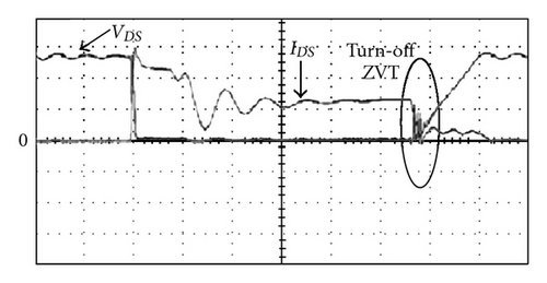
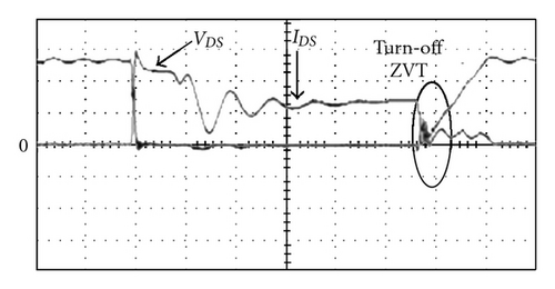
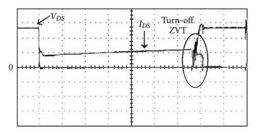
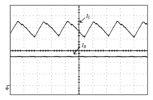
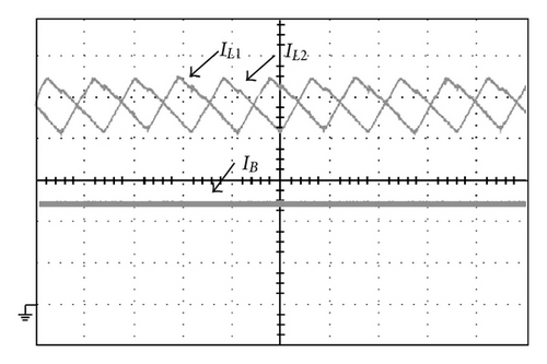
The measured voltage and current waveforms of the active switches with the proposed single-capacitor snubber (as shown in Figure 4) and with two sets of turn-off snubbers (as shown in Figure 3) are shown in Figures 15 and 16, respectively. Although we can observe that each power switch is turned off with ZVT feature, there still exist significant differences. Compare with Figures 15 and 16, we can see that the rise voltage curves of Figure 15 are smoother than those of Figure 16. The reason of this is that interleaving boost converter with two sets of turn-off snubbers, causes an abrupt energy on active switches and results in more switching losses. Figure 17(a) shows measured inductor current and charging current of the single boost converter with a turn-off snubber, and Figure 17(b) shows measured inductor current and charging current of the proposed interleaved boost converter with a single-capacitor turn-off snubber. From Figure 17, it can be seen that the proposed converter with a single-capacitor turn-off snubber has a lower ripple charging current IB.
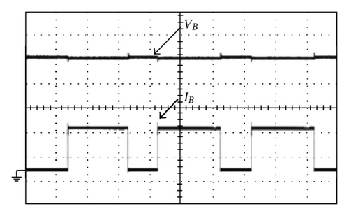
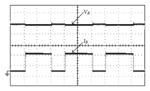
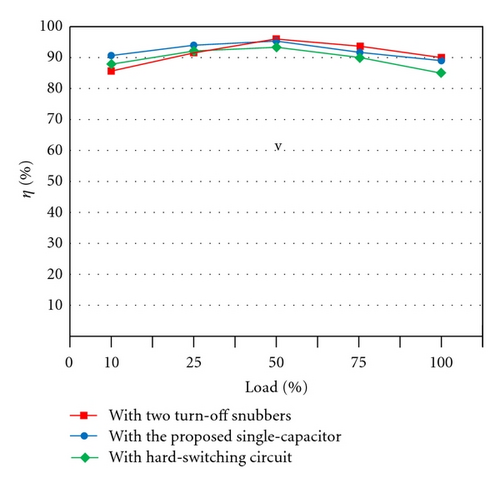
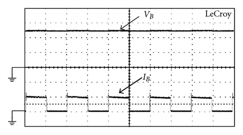
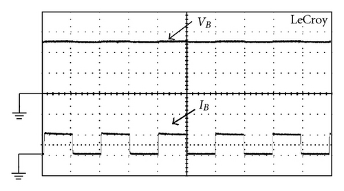
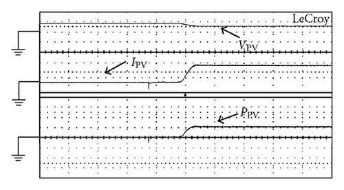
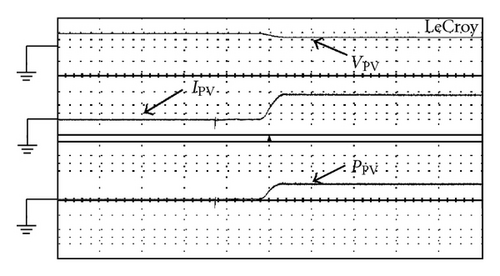
To make a fair comparison, the hardware components of the proposed charger and hard-switching boost charger are kept as the same as possible. Figure 18 shows the plots of output voltage and current waveforms of the two kinds of chargers under step-load changes between 20% and 100% with, respectively, rate of 1 kHz and a duty ratio of 50%. From Figure 18, it can be observed that although the proposed charger uses less component counts, it yields almost the same dynamic performance as those with complicated configurations. The comparisons between the efficiencies of the proposed charger and their counterparts are illustrated in Figure 19. It can be observed that the proposed charger cannot always yield higher efficiencies than the others under various operating conditions. It has a trend that, at higher output load, the proposed charger and the ones with two turn-off snubbers can yield higher efficiency, while at lower ones, the discussed charger with two sets of turn-off snubbers yields lower efficiency than the others. The reasons behind this are that at a fixed power level, a higher output load level will result in higher switch currents and the turn-off losses WSoff will be much higher than the sum of the extra conduction loss WES and switching loss WSon . Figure 20 shows the measured waveforms of battery voltage VB and charging current IB with pulse current charging method under repetitive rate of 1 s and duty ratio of 500 ms, as shown in Figure 14. Figure 20(a) shows those waveforms under PPV(max ) = 50 W, while Figure 20(b) illustrates those waveforms PPV(max ) = 100 W. From Figure 20, it can be seen that maximum pulse charging current IO(max ), respectively, is limited 1 A (about 0.15 C) and 2 A (about 0.3 C), where battery adopts lead-acid battery and capacity of each battery is 12 V/7 Ah and total battery voltage is 50 V. Measured waveforms of voltage VPV, current IPV and power PPV of PV arrays with perturbation-and-observation method are used to implement MPPT. Figure 21(a) shows those waveforms under maximum power point PPV(max ) at 100 W, while Figure 21(b) depicts those waveforms under PPV(max ) at 200 W. From Figure 21, it can be found that tracking time of PV arrays from zero to the maximum power point is about 40 ms.
6. Conclusions
In this paper, an interleaving boost converter with a passive snubber for battery charger applications is proposed. The proposed charger with a single-capacitor snubber to reduce voltage stresses of active switches at turn-off transition. Therefore, the conversion efficiency of the proposed charger can be increased significantly. In order to draw maximum power from the PV energy, a simple perturbation-and-observation method is incorporated to realize maximum power conversion. To verify the merits of the proposed charger, the operational principle, steady-state analysis, and design considerations have been described in detail. Additionally, from the experimental efficiency of the proposed charger, it has been shown that the proposed charger can yield higher efficiency at heavy load condition. An experimental prototype for a battery charger application (540 W, 54 Vdc/10 A) has been built and evaluated, achieving the efficiency of 88% under full load condition. Therefore, the proposed interleaving boost converter is relatively suitable for battery charger applications.


