FFT Analysis of a Series Loaded Resonant Converter-Based Power Supply for Pulsed Power Applications
Abstract
An impulse power supply has been designed, simulated, and tested in order to feed the primary of a high-frequency transformer. Pulse power system has been widely used for plasma applications. The operational principle of the pulse power system is that the energy from the input source is stored in the capacitor bank device through a dc-dc converter. Then, when a discharging signal is given, the stored energy is released to the load. The new family of ZCS converters is suitable for high-power applications using insulated gate bipolar transistors (IGBTs). The power converter can achieve zero switching with the aid of high-frequency transformer. The device is capable of charging a 0.1 μF capacitor up to 5 kV which accounts for a charging power of 5 kJ/s. The novel control algorithm is achieved which eminently considers the nonlinear control characteristics of impulse power supply. The required charging voltage, together with the constraint on the charging time, translates into a required maximum power of 10 kW reduced in this initial version to 5 kW. The difficulty to reliably control such a power at the high-voltage side practically forbids any approach featuring a more or less stabilized DC high-voltage to be generated from a conventional 50 Hz transformer through rectification.
1. Introduction
For many years, power electronics in the high-power area was performed with slow semiconductor switches like MOSFET and BJT. The IGBT is a relatively new power semiconductor device, which provides the best features of both the MOSFET and the BJT [1]. Its advantages are low power, voltage-driven turn on and turn off, gate impedance as high as MOSFET, low-conduction losses, and positive temperature coefficient. The device will not experience thermal run-away as of BJTs. Possibility to use either integrated or external antiparallel diode. Recent improvements in high-power semiconductor technology have given switching performance similar to that of the IGBTs to the high-power area through the advancement of the IGBTs. This paper explains the internal dynamics [2] of IGBT behavior in zero current switching circuit topologies. The impulse power supply described in this paper has been initially built to provide a charging power of 5 KW only. The impulse power supply differs from conventional power supply in that capacitor charging requires operation over a wide range of load conditions varying from nearly short circuit, when the capacitor has no charge, to nearly open circuit, when the capacitor is almost fully charged. This kind of performance can be best achieved by supplying a constant charging current. The instantaneous output power then is minimum at the charge beginning and maximum at the charge end. The paper proposes a novel topological circuit of stable voltage source power converter using latest IGBTs (IRG4PH40PUD).
2. System Design
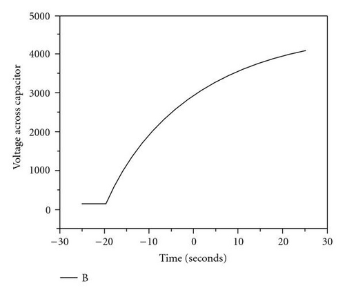
The required charging voltage, together with the constraint of the charging time, translates into a required maximum power of 10 KW reduced in this initial version to 5 KW as shown in Figure 1. The difficulty to reliably control such a power at the high-voltage side practically forbids any approach featuring a more or less stabilized DC high-voltage to be generated from a conventional 50 Hz transformer through rectification, as shown in Figure 2.
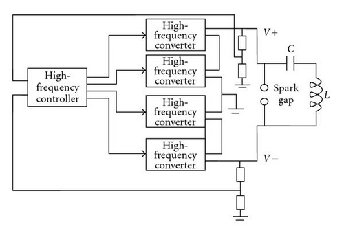
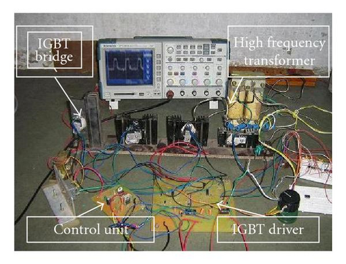
Instead, it is more attractive to utilize a high-frequency converter performing the regulation at the low-voltage side of its step-up transformer and charging the primary capacitor with high-voltage pulses. Such a device is not capable of providing a stabilized DC voltage and, therefore, can be merely regarded as an impulse power supply. The modular architecture allows simplifying the problem of the construction of the 20 KV, 5 KW step-up transformers and the selection of electronic components suitable to drive it. A subdivision of the power supply into four identical blocks reduces the requirements to four 5 KV, 1.25 KW modules, which can be implemented with off-the-shelf components.
The design is scalable, as more converter modules can be added in series to reach a higher charging voltage, with their output floating respect to ground. The capacitor charging power supply (CCPS) output is internally center-tapped to ground one of the output leads. Hence it assumes a maximum potential of +10 KV while the other one assumes a minimum potential of −10 KV (respect to ground). This strategy increases safety and allows reducing to one half (10 KV DC) the insulation requirement of assemblies and wiring. A single controller module samples the charging voltage and drives the converter. It is responsible for synchronizing the charge with external events and suspending the charging pulses when a predetermined voltage is reached. Galvanic isolation at several points is either required or desirable in order to reduce noise and interference.
3. High-Frequency Converter
The basic block diagram of one converter module as shown in Figure 3. The converter modules are fed with 560 V DC obtained by rectifying 400 V AC from the mains. A full-bridge switch drives a step-up transformer with a 9 : 1 turns ratio in order to reach a rectified output voltage of about 5 KV DC. The switch commutation is externally driven by the controller (UC3860) module, according to the capacitor charge state as shown in Figure 4.
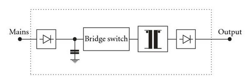
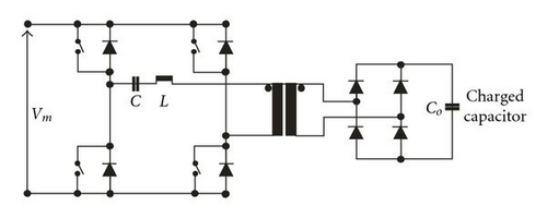
The topology selected for the converter is the series-loaded resonant (SLR) [3, 4]. In this configuration, the switches and resonant components L and C are connected to the low-voltage side of the transformer. Only the rectifiers on the transformer secondary must have high-voltage ratings. By closing, in proper order, the switches in pairs, pulses of alternate polarity are applied to the transformer using a high-turn ratio, high-voltage pulses are generated at the secondary, increasing the capacitor charge.
4. Theory of Operation
Therefore, Z0 and f0 are uniquely defined by C and L. Operating the circuit at a frequency fs < f0/2, all switches and antiparallel diodes turn on and off at zero current. Using a frequency f0/2 < fs < f0, the diodes turn off and the switches turn on happen at a current greater than zero. Conversely, for fs > f0, the diodes turn on and the switches turn off at a current greater than zero [9].
5. Results
This value is reached only at the end of the charge and is due to the energy accumulated in the resonant load C2 and L1 at charge beginning is ION = −IOFF max . Therefore, the SLR converter switches must be capable to stand ION max , while the diodes can be sized to operate at IOFF max only:
The theoretical power value as per (11) is more than sufficient to ensure an actual value greater than the targeted 1.25 KW.
For approximate analysis using complex ac-circuit analysis [10–13] in this method, fundamental components of the waveforms are used for voltages and currents. This method cannot predict the various voltage and current waveforms appropriately, and the accuracy reduces as the switching frequency is away from resonance frequency (as in variable frequency-controlled converters) or as the duty ratio decreases (as in fixed frequency-controlled converters).
For Fourier series method or frequency domain approach [12, 13] method, all the predominant harmonics are taken into account. This method is simple and gives good results.
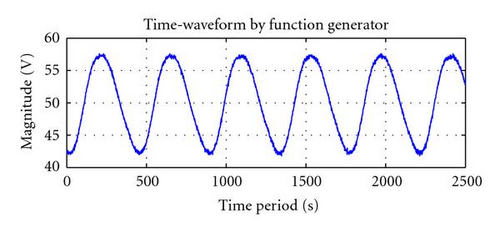
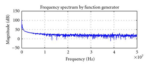
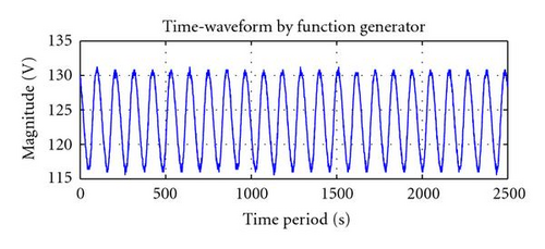
The output wave form is taken on the TPS2014 digital storage oscilloscope. The output voltage of transformer is as shown in Figure 5. The signal via digital storage oscilloscope (DSO) is analyzed in FFT toolbox of MATLAB. The commutation takes place at zero current; unwanted spikes and noise are present due to parasitic capacitance, PCB traces impendence, reverse recovery time of the antiparallel diodes, electromagnetic radiation, and coupling within the converter PCB. The noise signal can be seen from the fft wave form.
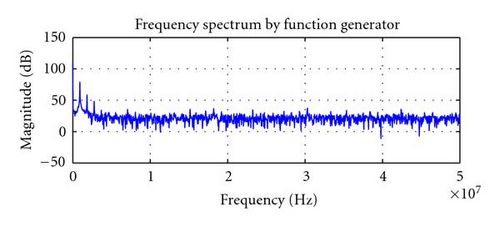

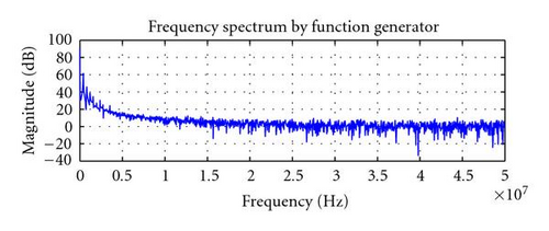
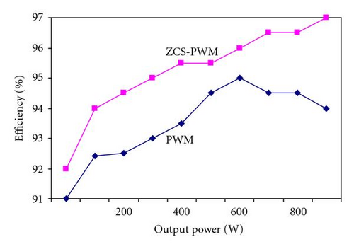
The maximum peak reverses current flowing through the diode when one pair switch is open is −13 amps. The ION max is 26 amps. From Figure 9, we can see that the efficiency of ZCS-PWM is much better [14] than that of ordinary PWM because the losses in the ZCS decrease due to soft switching.
6. Conclusion
With the new device technology recently developed, the performance of high-power converters can be improved dramatically in terms of dynamics, efficiency, size, and protection, due to the improved switching speed and the removal of the turn-off snubber. The series load resonant topology choice for the switching converter module resulted in minimized switching loss and reduced size of the heat sink. The proposed schemes have several advantages over conventional scheme such as simple operation, easy analysis and control, and improved effiency.


