Highly Emissive Lanthanide-Based 0D Metal Halide Nanocrystals for Efficient Ultraviolet Photodetector
Abstract
Recently, lanthanide-based 0D metal halides have attracted considerable attention for their applications in X-ray imaging, light-emitting diodes (LEDs), sensors, and photodetectors. Herein, lead-free 0D gadolinium-alloyed cesium cerium chloride (Gd3+-alloyed Cs3CeCl6) nanocrystals (NCs) are introduced as promising materials for optoelectronic application owing to their unique optical properties. The incorporation of Gd3+ in Cs3CeCl6 (CCC) NCs is proposed to increase the photoluminescence quantum yield (PLQY) from 57% to 96%, along with significantly enhanced phase and chemical stability. The structural analysis is performed by density functional theory (DFT) to confirm the effect of Gd3+ in Cs3Ce1-xGdxCl6 (CCGC) alloy system. Moreover, the CCGC NCs are applied as the active layer in UVPDs with different Gd3+ concentration. The excellent device performance is shown at 20% of Gd3+ in CCGC NCs with high detectivity (7.938 × 10¹¹ Jones) and responsivity (0.195 A W−1) at -0.1 V at 310 nm. This study paves the way for the development of lanthanide-based metal halide NCs for next-generation UVPDs and other optoelectronic applications.
1 Introduction
Lanthanide-based 0D metal halides (Cs3LnX6, Ln = lanthanide, X = Cl, Br) have garnered considerable attention for their application in X-ray imaging, light-emitting diodes (LEDs), sensors, etc.[1-3] In particular, the parity-enabled 4f–5d transitions of Ce3+, Eu2+, and Yb2+ ions make these materials potential candidates for optoelectronic applications.[4] For example, Wang et al. fabricated ultraviolet (UV) LEDs using non-toxic Cs3CeBr6 metal halide films.[5] It is noteworthy that the reported fabrication process for the emissive layer is limited to thermal evaporation. Nanocrystals are ideal for solution deposition methods, providing advantages such as large-area coating, easy scale-up, and low cost.[6] Therefore, fundamental research is required to explore the application of lanthanide ions in optoelectronic devices using solution-based processes.[7] This enables us to perform a comprehensive analysis of the inherent crystalline and optical properties of the material, providing a deeper understanding of the potential of lanthanide ions in optoelectronic devices.
Photodetectors (PDs) that convert incident photons into electrical signals have applications in various fields, such as optical communication, biological sensing, military-grade applications, and imaging.[8-11] Specifically, ultraviolet photodetectors (UVPDs), which absorb broad UV light and convert it to electrical signals, are indispensable for guided weapons, secure communication, wide spectral switches, atmospheric monitoring, and many other applications.[12-15] Materials such as silicon (Si) and semiconductors like II–VI and III–V group compounds (SiC, Ga2O3, GaN, and AlGaN) have been extensively investigated owing to their superior efficiency.[16-19] However, their high fabrication costs and limited flexibility present significant restrictions for wearable applications.[20] As an alternative, lead halide perovskites (LHPs) have attracted considerable attention for broadband UVPDs owing to their high absorbance coefficient, broad absorbance band, and high charge carrier mobility.[21-24] However, the main drawback of LHPs is the high toxicity of lead.[25] In the search for lead-free metal halide groups, such as CsSnX3, Cs3Bi2X9, Cs3Sb2X9, and Cs2AgBiX6 (X = Cl, Br, or I), have emerged as prominent materials.[26-30] However, these materials lack a high photoluminescence quantum yield (PLQY) because of various defects and oxidation to cations. Therefore, an urgent need exists to develop new lead-free metal halides for application in UVPDs.
In this study, we synthesized Cs3CeCl6 (CCC) nanocrystals (NCs) via a hot injection method and achieved a significant enhancement in their optical properties and stability via partial substitution of Ce3+ by Gd3+ ion. The incorporation of Gd3+ ions into the CCC NCs resulted in not only a uniform size distribution, with an average particle size of 18 nm, but also the significant increase in photoluminescence (PL) quantum yield from 57% to 96%. To characterize the additional influence of Gd3+ alloying in CCC NCs on PDs, we examined their thermal quenching properties and temperature-dependent PL with exciton binding energies. To comprehend our experimental findings, fundamental study was performed by first principle calculations to track positions which Ce3+ and Gd3+ can occupy in a same crystal structure. Subsequently, ultraviolet photodetectors (UVPDs) were fabricated with the CCC, and the CCGC NCs, using spin coating. Finally, the CCGC NCs UVPD demonstrated excellent performance, with excellent detectivity (7.938 × 10¹¹ Jones) and responsivity (0.195 A W−1) at 310 nm.
2 Results and Discussion
2.1 Structural and Morphological Characterization of CCC and CCGC NCs
The main objectives of this study were to develop CCC NCs by Gd3+ alloying and to combine experimental and theoretical studies to better understand their structural, optical, and optoelectronic properties. The CCC NCs synthesized via the hot-injection method have a monoclinic structure with C2/c space group consisting of [CeCl6]3- octahedra and a Ce atom attached to six Cl atoms. The bond lengths between Ce and Cl in each octahedron (labeled Ce1 and Ce2) are shown in Figure 1a, indicating the presence of two different octahedra within the 0D structure. However, CCC NCs suffer from low stability as Ce3+ ions undergo quick oxidation to Ce4+ because of their relatively negative reduction potential under ambient conditions compared to other Ln3+ ions, such as Tb3+ and Pr3+.[4] Therefore, the smaller Gd3+ ion is suitable to alloy for enhancing the stability and optical properties of CCC NCs. Monoclinic Cs3GdCl6 (CGC) has the same crystal structure and X-ray diffraction (XRD) pattern as CCC, as shown in Figure S1 (Supporting Information).[3] Structural analysis of the CCGC NCs with 50% Gd3+ was performed via Rietveld refinement of the XRD patterns using GSAS software with refinement parameters.[31] The refined XRD pattern is illustrated in Figure 1b. The XRD pattern of the 20% Gd3+-alloyed CCGC NCs was also refined, as shown in Figure S2 (Supporting Information). The values of the refinement parameters indicate the formation of single-phase CCGC NCs in both 20% and 50% Gd3+ without any impurities. Detailed Information related to Rietveld refinement is presented in Tables S1–S3 (Supporting Information).

These results show that 50% Gd3+-alloyed CCGC NCs have smaller lattice parameters than 20% Gd3+-alloyed CCGC NCs due to the slightly different ionic radius between Ce3+ and Gd3+ ions. As a result, the unit cell volume also decreases as the ratio of Gd3+ increases in Cs3Ce1-xGdxCl6. The cell volume and lattice parameters change in the stable composition of CCGC NCs at different Gd3+ concentrations were compared with the calculation based on Vegard's law in Figure S3 (Supporting Information). The slight deviation from Vegard's law at 0.5 can be attributed to the fact that Ce only occupied the 4d site and Gd only occupied the 4e site in the structure. Further details are discussed in the section on crystal structural study. These are distinct evidence to support that the site for Ce3+ can be occupied by Gd3+. Figure S4 in Supporting Information shows that the XRD patterns of the pure CCC NCs are identical to those of the CCGC NCs. Elemental analysis of the CCC and 50% Gd3+-alloyed CCGC NCs was performed via X-ray photoelectron spectroscopy (XPS), as shown in Figure 1c. The XPS spectra obtained by CCC reveal the presence of Ce (4d) and Cl (2p) elements. However, for the 50% Gd3+-alloyed CCGC NCs, a supplementary peak corresponding to Gd (4d) was observed in addition to the Ce and Cl peaks. This indicates the incorporation of Gd3+ into the CCGC NCs. In addition, a decrease in the XPS counts of Ce (5d) was observed in proportion to the ratio of Gd3+ in the CCC NCs, indicating that Gd3+ occupying occurred at the Ce site. The high-resolution XPS profiles of CCC NCs and 50% Gd3+-alloyed CCGC NCs for Ce (3d), Gd(4d), and Cl (2p) are added in Figure S5 (Supporting Information). The 2p3/2 energy level containing four electrons in CCGC NCs (50% of Gd3+) shows a higher binding energy compared to CCC NCs. This result suggests the substitution of Ce3+ by Gd3+ because of a stronger bond between Gd3+ and Cl− from competition between Ce3+ and Gd3+ to occupy the center site in [CeCl6]3− octahedra.
Subsequently, the morphology of the 50% Gd3+-alloyed CCGC NCs was analyzed using transmission electron microscopy (TEM), as shown in Figure 1d. The TEM images demonstrate that the average particle size of the 50% Gd3+-alloyed CCGC NCs is approximately 18 nm, with a narrow particle size distribution. Figure 1e shows a high-resolution transmission electron microscopy (HR-TEM) image of the CCGC NCs with a lattice plane distance of 0.29 nm. The calculated lattice plane distance matches the (422) plane of the CCGC crystallographic data. The selected area diffraction (SAED) patterns shown in the inset of Figure 1e, are well matched with the crystallographic data. Energy-dispersive spectroscopy (EDS) mapping, as shown in Figure 1f, further confirmed the presence of Cs, Cl, Ce, and Gd throughout the CCGC NCs.
2.2 Optical and Morphological Characterization of CCGC NCs in Different Alloying Concentration
The optical and morphological properties of the CCC NCs with different alloying ratios of Gd3+ ions are presented in Figure 2 for analysis. The excitation and emission spectra of CCC, along with its luminescence mechanism, are shown in Figure 2a. Upon UV excitation, CCC NCs emitted intense luminescence in the UV to visible region, described as asymmetric luminescence bands at 376 and 408 nm. For the Ce3+ ion, the 4f1 energy level splits into 2F5/2 and 2F7/2 by a spin–orbit coupling, while the 5d1 (2D) energy level splits into T2g and Eg as a result of crystal field effect.[32, 33] The major luminescence bands at 379 nm and 408 nm originated from the transition from the lowest 5d1 (T2g Γ8) to the 4f1 (2F5/2 and 2F7/2) multiples.[34] The excitation spectra of the CCC NCs were measured by monitoring the 376 nm luminescence band. Excitation bands were observed at 264 and 336 nm, which are attributed to the 4f–5d electronic transition.[35] A well-known characteristic of Ce3+-based luminescent materials is their parity-allowed f–d transition exhibited by Ce3+ ions, typically showing a broad emission band, short PL lifetime (usually on the nanosecond scale), and a tunable emission spectrum, which are promising properties for optoelectronic devices.[4] The [CeCl6]3− octahedra, including Cl− ions as ligands, which has a dominant effect on the crystal field splitting strength, exhibits a sixfold coordination number, indicating strong splitting in the 5d of Ce3+ ions.[36, 37]
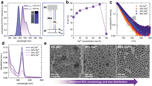
We observed a gradual increase in the PLQY of the CCC NCs with an increase in the Gd3+ concentration, as shown in Figure 2b. The highest PLQY of the CCGC NCs was 96% when the Gd3+ concentration was 80% Figure S6, Supporting Information). This represents a substantial enhancement compared to the initial PLQY of 57% without Gd3+. This improvement of PLQY is attributed to the substitution of Ce3+ ions with Gd3+ ions in [CeCl6]3− octahedra, indicating the suppression of concentration quenching by providing higher distances between Ce3+ ions and reducing radiation reabsorption.[38] However, after the complete substitution of Ce3+ with Gd3+ ions, the PLQY of the CGC NCs decreased to 6.2%, which is attributed to the surfactant ligands. This is because Gd3+ ions are not attributed to the energy transition in the UV region as shown in Figure S7 (Supporting Information) for the partial density of state (PDOS) of CGC, showing no electronic state gap. The only possible reason why CGC NCs give emissions in the UV region would be oleic acid and oleylamine on the surface of NCs. Moreover, the time-resolved photoluminescence (TRPL) decay of the CCC and CCGC NCs was measured upon excitation at 316 nm, and the emission peak at 380 nm was monitored, as shown in Figure 2c. The parameters of the decay curves are listed in Table S4 (Supporting Information). The average lifetime of the CCC NCs increased with the Gd3+ concentration. The fitted average lifetimes are 26.5 ns, 32.9 ns, 35.0 ns, and 42.8 ns for 0%, 20%, 40%, and 80% of Gd3+ ions in CCGC NCs, respectively. This further explains the improvement in the PLQY of CCGC NCs with increasing Gd3+. As shown in Figure 2d, the CCC NCs have significant absorbance in the UV-A region between 300 and 400 nm, with a peak at 334 nm. The full width at half maximum (FWHM) of the absorbance peak is 27 nm for the CCC NCs with good selectivity, indicating that the CCC NCs can serve as effective absorbing layers for UVPDs. However, the absorbance intensity decreased with increasing Gd3+ concentration in the CCGC NCs. This is because the energy transition at the UV region occurs only from 5d and 4f orbital states of Ce3+ ions as the Gd3+ does not contribute to the bandgap, as shown in Figure S11 (Supporting Information). This decrease in absorbance at 334 nm supports that Gd3+ ions substitute for the site of Ce3+ according to the alloying ratio.
Interestingly, Gd3+-alloyed CCGC NCs improved the optical properties and the morphology and particle size distribution, as shown in Figure 2e. Moreover, the average particle size of the CCGC NCs decreases from 29 to 18 nm with an increase of Gd3+ concentration from 0 to 50%. Consequently, the FWHM of the size distribution reduced from 11.1 nm to 3.2 nm (Figure S8 in Supporting Information). Note that the monodispersity with narrow FWHM in size distribution is beneficial to obtain a more uniform film without voids and pinholes with enhanced device performance.[39] However, excessive Gd3+ (more than 50%) adversely affects the morphology and size distribution of the CCGC NCs, as depicted in Figure S9 (Supporting Information). Computational calculations were conducted to comprehend the underlying mechanism of the improved properties of CCGC NCs.
2.3 Crystal Structural Study and Optical Stability of CCGC NCs
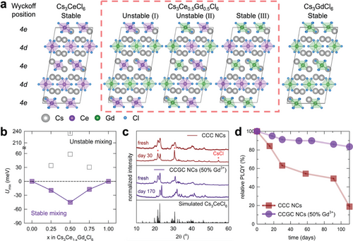
The XRD patterns of the CCGC NCs shown in Figure 3c confirm the superior phase stability of the 50% Gd3+-alloyed CCGC NCs compared with that of the pristine CCC NCs. The CCC NCs exhibited poor stability within 30 d of storage under ambient conditions, corresponding to the additional CsCl XRD peaks observed. In contrast, the 50% Gd3+-alloyed CCC NCs exhibited superior stability over 150 d under ambient conditions. The optical stability of the CCGC NCs was analyzed using PLQY measurements, as shown in Figure 3d. The initial PLQY of the CCC NCs decreased by 50% after 84 d. For the 50% Gd3+-alloyed CCC NCs, 84% of the initial PLQY was maintained after 110 d. These enhanced phase and optical stability of the CCC NCs were achieved by alloying with Gd3+, which is crucial for optoelectronic device fabrication.
2.4 Electrical Characterization of CCGC NCs for Photodetector
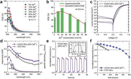
As mentioned previously, CCC NCs exhibit high absorbance in the UV-A region, making them good candidates as absorbers in PDs. The absorbance and PLQY of the absorbing layer in PDs are crucial factors determining device performance due to their significant contribution to photocurrent generation. We performed a calculation to estimate the relative external quantum efficiency (EQE) of the PD as a function of the Gd3+ concentration in the CCC NCs, and the two factors were assumed as the main parameters. The best performance of the PDs was predicted to be at approximately 20% of the Gd3+ concentration, as indicated in Figure 4a with a red line according to the tradeoff relation between the relative PLQY and absorbance. In addition, we verified whether the best performance is achieved with the 20% Gd3+ by comparing our calculation with experimental results obtained from fabricating a series of devices in Figure 5.
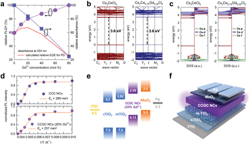
Furthermore, we calculated the electronic structures using CCC and CCGC to understand the electronic consequences of Gd3+ incorporation. As shown in Figure 4b, both CCC and CCGC exhibit a direct optical bandgap of 3.6 eV at the gamma point without a significant change in their band structure near the band edges. Indeed, despite the incorporation of Gd3+ into the CCC lattice, the conduction band minimum (CBM) of CCC and CCGC was contributed to the Ce-5d orbital while the valence band maximum (VBM) consisted of the Ce-4f orbital (Figure 4c). This can be attributed to the fact that the Gd3+ ions do not introduce electronic states in the bandgap of CCC, but form electronic states far away from the band edge of CCC (see Figure S11 in Supporting Information). A concentration of 25% was selected for the DFT calculations, based on the results of the EQE estimation. It was confirmed that the spin- and parity-allowed 4f–5d transition in Ce3+ demonstrated a nanosecond-scale PL lifetime, which has significant advantages for optoelectronic devices.
To verify the calculated relative EQE values, charge transport layers (CTLs) were selected to design the full photodiode-type device based on the energy-level diagram of the CCGC NCs. Therefore, the VBM of the 20% Gd3+-alloyed CCGC NCs was determined using ultraviolet photoelectron spectroscopy (UPS) measurements in Figure S15 (Supporting Information). Subsequently, the optical bandgap (3.53 eV) was estimated based on the UV–Vis absorbance spectrum using the modified Kubelka–Munk equation in Figure S16 (Supporting Information).[45] Accordingly, the energy level diagram of the PD is shown in Figure 4e, including the optimum CCGC (20% Gd3+) NCs with the calculated VBM (6.12 eV) and CBM (2.59 eV). The CTLs were selected by considering the energy level of the CCGC NCs to reduce the energy barriers so that charges could be extracted efficiently.[46] The device structure consisted of fluorine-doped tin oxide (FTO), compact titanium dioxide (c-TiO2), mesoporous titanium dioxide (m-TiO2), absorbing layer (CCGC NCs), molybdenum trioxide (MoO3), and silver (Ag), as shown in Figure 4f. FTO was used as the cathode, c-TiO2 and m-TiO2 as electron-transport layers (ETLs), MoO3 as the hole transport layer (HTL), and Ag as the anode.
Finally, we monitored R values to investigate the operational stability of the fabricated PDs during storage of the devices in an N2-filled glovebox. As depicted in Figure 5f, compared to CCC PD, the PD based on CCGC (20% Gd3+) exhibited much more improved stability by maintaining 80% of its initial R-value for up to 370 h. CCGC NCs possess enhanced electrical durability due to phase stability and reduced internal energy. For comparison with prior research, we compiled the parameters of lead-free metal halide-based UVPDs in the region (200–400 nm), as summarized in Table S5 (Supporting Information).
3 Conclusion
Lead-free 0D CCC NCs were successfully synthesized using the hot-injection method. The CCC NCs exhibited a significantly narrow absorbance spectrum with good selectivity in the UV-A region. Furthermore, Gd3+ alloying in the CCC NCs resulted in a significant PLQY and improved phase stability. The PLQY of the CCC NCs was improved from 57% to 96% by increasing the Gd3+ concentration. Crucially, our investigations revealed a direct correlation between the alloying ratio and the phase stability of CCC NCs. Using both density functional theory (DFT) calculations and experimental findings, we illustrate the distinct preferences of Ce3+ and Gd3+ ions to occupy sites (4d and 4e) within the same crystal structure, resulting in reduced internal energy and thermodynamically enhanced phase stability at a 50% alloying level. Consequently, we employed external quantum efficiency (EQE) calculations for photodetectors (PDs) to determine the optimal Gd3+ percentage in the CCC NCs, considering the trade-off between PLQY and absorbance. Both experimental and calculated results indicated that the peak performance was achieved with CCC NCs alloyed with 20% Gd3+, exhibiting remarkable detectivity (7.938 × 10¹¹ Jones) and responsivity (0.195 A W−1) at a -0.1 V bias. This study marks a pioneering exploration into the utilization of lanthanide metal halide NCs for ultraviolet photodetectors (UVPDs). The outcomes of this study not only contribute to the understanding of developing lead-free lanthanide-based materials but also hold promise for future applications.
4 Experimental Section
Materials
Cesium carbonate (Cs2CO3, 99%), cerium acetate (99%), gadolinium acetate (99%), 1-octadecene (ODE, 99%), oleic acid (OA, 90%), oleylamine (OLA, 98%), benzoyl chloride, ethyl acetate, hexane (anhydrous, 95%), and octane (reagent grade, 98%) were purchased from Sigma-Aldrich. Titanium diisopropoxide bis(acetylacetonate) and 2-methoxyethanol (anhydrous, 99.8%) were purchased from Sigma-Aldrich. Ethyl alcohol (anhydrous, 99.9%) and α-terpineol (C10H18O) were purchased from SAMCHUN and DAEJUNG, respectively. TiO2 paste (SC-HT040) was purchased from ShareChem.
Synthesis of Cs3Ce1-xGdxCl6 Nanocrystals
Cs3Ce1-xGdxCl6 nanocrystals were synthesized using the hot injection method. 0.3 mmol of Cs2CO3 and 0.2 mmol of cerium acetate were degassed in a three-neck flask with ODE under vacuum at 120 °C for 1 h. Cerium acetate can be substituted with gadolinium acetate according to the alloying concentration. Subsequently, the flask was filled with N2 gas. 2 mL of OA and OLA were injected into the flask, and the temperature was raised up to 200 °C until the mixture completely dissolved. Then, 0.3 mL of benzoyl chloride was quickly injected to react for 10 s, and the flask was cooled down in an ice bath. The crude solution was centrifuged at 8000 rpm for 10 min. The precipitated nanoparticles were dispersed in 10 mL of hexane, and a mixture of ethyl acetate and hexane in a 2:1 volume ratio was added. The solution was then centrifuged at 8000 rpm for 5 min. Finally, the precipitate was dispersed in octane and centrifuged at 4000 rpm for 10 min to obtain a suspension of well-dispersed nanoparticles in the supernatant.
Device Fabrication
The patterned fluorine-doped tin oxide (FTO) glass substrates were cleaned by sonication in detergent deionized water, acetone, and isopropyl alcohol for 15 min. After cleaning, the blocking layers of TiO2 (c-TiO2) were then deposited onto cleaned substrates by spray pyrolysis deposition using titanium diisopropoxide bis (acetylacetonate) solution (Aldrich) at 450 °C. Then, mesoporous TiO2 (m-TiO2) films were spin-coated onto the FTO/c-TiO2 substrates and were annealed at 500 °C for 1 h. Subsequently, CCC or CCGC NCs were spin-coated at 800 rpm for 60 s. Finally, 7 nm thick MoO3 and 100 nm thick Ag electrodes were deposited by thermal evaporation under vacuum of 10−6 Torr.
Structural and Morphology Characterizations
The structures of the as-synthesized samples were characterized by XRD (Miniflex 600) using a diffracted beam monochromator set for Cu-Kα radiation (λ = 1.54056 Å). The 2θ scan range was 10°–60° with a step size of 0.01°. Structural information was derived from Rietveld refinement using the GSAS software suite.[31] A 0D visualization system for electronic and structural analysis (VESTA)[50] was used to draw the crystal structures. The phase purity of the as-synthesized samples was estimated via Rietveld refinement of the XRD results with the consideration of full refinement of the crystallographic and instrumental parameters in the GSAS program suite. HR-TEM images and energy-dispersive X-ray spectroscopy (EDS) were obtained using a JEOL JEM2100F microscope.
First Principles Density Functional Theory Calculations
The underlying density functional theory (DFT) calculations were performed using the Vienna Ab initio Simulation Package (VASP).[51, 52] Projector augmented-wave (PAW)[53, 54] pseudopotentials were employed to treat core atomic states where the valence electron configurations of Cs, Ce, Gd, and Cl were explicitly considered as 5s25p66s1, 4s24p64f15d16s2, 4s24p64f75d16s2, and 3s23p5, respectively. The Perdew-Burke-Ernzerhof exchange-correlation functional (PBE)[55] with, the use of a Hubbard U correction[56] was used to consider the strong Coulomb repulsion for the Ce-4f and Gd-4f electrons (GGA+U with Ueff = 3.4 eV for Ce and 6.0 eV for Gd). The primitive unit cell of Cs3Ce1-xGdxCl6 was adopted that contains 44 atoms. The plane-wave kinetic energy cutoff of 700 eV was employed while the Brillouin-zone integrations were performed with a Γ-centered k-point grid of 4 × 4 × 4. Convergence criteria were set of 10−6 eV and 10−2 eV Å−1 for total energies and forces on each atom, respectively during structure optimizations.
Optical Characterizations
Steady-state PL spectra of the samples were recorded using a Hitachi F-7000 fluorescence spectrophotometer. X-ray photoelectron spectra (XPS) of the samples were measured in Thermofisher Scientific (Nexsa G2) instrument. Thermofisher scientific Nexsa is a fully integrated XPS instrument, with low power Al Ka X-ray source, 10–400 µm (adjustable in 5 µm steps), 3600 mm2 (600 mm × 600 mm) sample area, 20 mm sample thickness. The absolute PLQY of the samples was measured using a HORIBA FluoroMax Plus spectrofluorometer paired with K-sphere petite internal, directly coupled with Integrating Sphere. The excitation source was standard 75 W xenon arc, attached to the front of QM sample compartment. The TRPL of the samples were measured using a HORIBA spectrophotofluorometer with TCSPC with pulsed nano LED 316 nm (±10 nm). The absorbance spectra of the samples were measured using Cary 5000 UV-Vis-NIR spectrophotometer. The UPS spectra of the samples were measured in Thermo Fisher Scientific (XPS-Theta Probe) instrument. The J–V curves were measured using a semiconductor analyzer (Keithley 4200-SCS), and TLS equipment consisting of a Xenon lamp (Newport, 450 W) and a monochromator was used as the light source. EQE spectra were measured using an incident photon-to-current conversion efficiency (IPCE) instrument (Compactstat, IVIUM) consisting of a monochromator and a Xenon lamp (Newport, 450 W). Response time curves were measured using oscilloscope (MSO5354, RIGOL) and TLS equipment as the light source.
Acknowledgements
J.W.M. and T.S. contributed equally to this work. This research was supported by a National Research Foundation of Korea (NRF) grant funded by the Korean government (MSIT) (RS-2024-00411892, NRF-2020M3H4A3081822), and the Samsung Research Funding & Incubation Center of Samsung Electronics under Project Number SRFC-TC2103-04.
Conflict of Interest
The authors declare no conflict of interest.
Open Research
Data Availability Statement
The data that support the findings of this study are available from the corresponding author upon reasonable request.


