Polycrystalline Diamond Micro-Hotplates
Abstract
Micro-hotplate structures are increasingly being investigated for use in a host of applications ranging from broadband infra-red sources within absorption-based gas sensors to in situ heater stages for ultra-high-resolution imaging. With devices usually fabricated from a conductive electrode placed on top of a freestanding radiator element, coefficient of thermal expansion (CTE) mismatches between layers and electro-migration within the heating element typically lead to failure upon exceeding temperatures of 1600 K. In an attempt to mitigate such issues, a series of hotplates of varying geometry have been fabricated from a single layer of mechanically robust, high thermal conductivity, and low CTE boron-doped polycrystalline diamond. Upon testing under high vacuum conditions and characterization of the emission spectra, the resulting devices are shown to exhibit a grey-body like emission response and reach temperatures vastly in excess of conventional geometries of up to 2731 K at applied powers of ⩽100 mW. Characterization of the thermalization time meanwhile demonstrates rapid millisecond response times, while Raman spectroscopy reveals the performance of the devices is dictated by cumulative graphitization at elevated temperatures. As such, both diamond and sp2 carbon are shown to be promising materials for the fabrication of next-generation micro-hotplates.
1 Introduction
The advent of micro-electro-mechanical systems (MEMS) and micro-fabrication technology has enabled the construction of micro-hotplate devices with miniaturized dimensions and thermal mass, offering localized heating with minimal power consumption and rapid thermal response time. Initially spurred on by the desire for low-power platforms within metal oxide gas sensors,[1-3] these devices have since been touted for use in applications ranging from IR sources within FTIR spectrometers or non-dispersive infra-red gas sensors[4-8] to heater stages for in situ electron microscopy materials characterization.[9, 10]
Typically, micro-hotplate structures consist of a meandering, electrically conductive element placed atop a SiN or SiO2 dielectric layer, with the underlying material locally removed to form either a closed membrane or a freestanding element held up by supporting beams.[9] Passing current through the conductive meander then results in Joule heating and a corresponding rise in temperature of the hotplate due to the large thermal isolation between substrate and freestanding device. For routinely reaching temperatures of up to 800 K, sufficient for the majority of sensing mechanisms used within solid-state gas detection,[1, 9] this heating element is typically fabricated from polycrystalline silicon or platinum.[2, 11] Attempts to push poly-Si based devices beyond these temperatures however leads to grain boundary diffusion and a corresponding degradation in device properties.[12] Meanwhile, platinum based devices often require an adhesion layer, adding complexity to the fabrication process, while the comparatively large coefficient of thermal expansion (CTE) of the metal and difference to that of other materials within the stack results in the formation of significant boundary-layer and compressive stress upon heating.[9, 11-13] When used for heating elements within high-magnification materials characterization, such high levels of stress combined with often sizeable thermal expansion can result in significant deflections of the hotplate, causing the sample under investigation to either move out of focus or out of the field of view of the microscope.[9] As temperatures surpass 1000 K, and into the range required by many of the aforementioned applications, the increasing stress then leads to rupturing of the stack and breakdown of the heating element through electro-stress migration of Pt atoms, with both effects exacerbated by temperature gradients across the device.[11, 14, 15] While the temperature at which these failure modes occur can be pushed higher by fabricating the meander from materials with higher melting point and CTE more closely matched to that of the insulating layer, namely Sb doped SnO2, Mo, TiN, and Ta5Si3, reaching temperatures beyond 1600 K with meander-on-insulator based designs remains challenging.[12, 13, 16, 17]
If the hotplates were instead fabricated from a single layer, this CTE-mismatch induced stress can be eradicated, allowing devices to operate closer to the melting point of the constituent materials. Deviating from traditional multi-layered geometries, micro-cantilevers fabricated from selectively-doped monocrystalline silicon have been shown to reach temperatures of up to 1600 K,[18, 19] while emission spectra captured during the biasing of freestanding polycrystalline SiC beams suggest temperatures approaching 1900 K.[20] Finite element modelling of polycrystalline silicon hotplates suspended from serpentine resistive arms has additionally shown uniform thermalization of the central radiating element when operating at 1200 K, suggesting that eradication of the separate meander element can also eliminate the often significant temperature non-uniformities observed with traditional hotplate structures.[11, 21-24]
Arguably the most promising materials to fabricate high operating temperature heat sources from are carbon allotropes or compounds thereof, with macro-scale 3D printed reduced graphene oxide filaments and micron-sized suspended graphene layers shown to reach temperatures of 3000 and 2900 K, respectively.[25, 26] The mechanical robustness, tailorable electrical and thermal conductivity, and low CTE afforded when carbon is sp3 hybridized thus makes diamond a particularly well suited material for the investigation of the element within freestanding micro-hotplate structures. Despite being optically opaque, the electron transparency of <100 nm thick boron-doped diamond tied with its chemical inertness also makes the material suitable for the fabrication of single material heater stages for use within ultra-high-resolution imaging, with the sample under investigation able to be placed directly in contact with the heating element to avoid any discrepancies in temperature.[10, 27] To date however, the extent of diamonds use within such devices has been as a heat-spreading layer to ensure uniform thermalization, or as a resistant capping layer for use in harsh environments.[28, 29]
The aim of this work is therefore to investigate the utilization of scalable, thin-film polycrystalline diamond (PCD) within single layer micro-hotplates. Emission from the resulting boron-doped PCD devices was characterized upon steady-state biasing through the use of two distinct optical setups, and the resulting temperatures extracted and cross-checked. The response of devices to transient signals was characterized while trends in device behaviour were then tied to structural changes through the use of Raman spectroscopy, comprehensively demonstrating the benefits and limitations of diamond based micro-hotplates.
2 Results
2.1 Structural Characterization and Design
Using the process detailed within the supplementary material a series of freestanding micro-hotplates with varying radiator size and arm geometry were fabricated from boron-doped PCD, with representative tilted images of the devices tested presented within Figure 1. The structures consisted of small and large octagonal elements with spans of 35 µm and 105 µm, respectively (panels A and C); and 50 × 50 µm square elements with either two or four arms (panels B and D). With the hotplates composed of a single uniformly-doped layer, Joule heating arises along the constrictive 3 µm wide supporting arms and flows outwards toward the radiator element and supports at either end. While the supports are thermally anchored to the substrate and able to dissipate this heat readily, the freestanding radiator elements are unable to do so, resulting in localized heating and radiative emission.[24] As such, heating is expected to be constrained to the single material elements of the device, preventing the formation of any CTE-induced stress at the multi-material anchor supports and averting the aforementioned issues commonplace within conventional structures. Arm geometries that compensate for expansion and contraction through elastic deformation of serpentine or spring-like tethers were used to support the elements in order to minimize thermal-mechanical stress and buckling observed when using four straight, axis symmetric arms.[7] Through meandering and tightly wrapping the arms around the periphery of the hotplate, larger resistances can also be created while keeping the overall footprint of devices to a minimum. The 3 µm diameter through holes in the radiator elements were meanwhile added to provide greater access to the sacrificial silicon underneath during the final release etch.
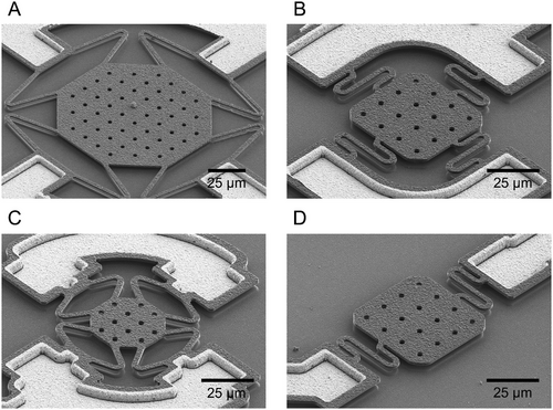
As to be expected given the high power density and low methane growth conditions, the doped polycrystalline diamond elements exhibits clear, randomly oriented faceting, with an average lateral grain size of the order of 500 nm and a roughness suggestive of van der Drift type competitive overgrowth.[30, 31] This morphology appears to remain unchanged during the step-edge transitions between the supports and the anchor trenches, with little evidence of the formation of pinholes, indicating uniform nano-diamond coverage of the substrate was achieved during seeding. Finally, the visible contrast overlaying these edges is a result of the Cr/Au bilayer used to minimize the resistance from hotplate to bond-pad and facilitate robust wire-bonding.
2.2 Electrical and Thermal Characterization
2.2.1 Octagonal Hotplates
To investigate the electrical and thermal properties of the devices, the emission from two sets of octagonal hotplates was first characterized through the use of a Raman microscope and a standalone monochromator while being subjected to biases from 1 V in increments of 0.25 V. Each bias point was held for 4 min to allow sufficient time for the monochromator to complete an entire sweep. The acquisition time of the spectrometer-based Raman system was meanwhile varied between 1 and 36 sec to prevent saturation of the detector and initiated 1 min into each hold. The resulting spectra obtained for the large octagonal hotplates are shown within Panels A and B of Figure 2 respectively, with the overlaid lines plotting the associated fits to Planck's law. The discontinuity in the monochromator data at 1050 nm coincides with the changing of the detector, grating, and order-sorting filter, and occurs as a result of the large difference in intensity correction factor applied either side of the transition and the variance in emission area between calibration source and hotplate device. As a result, each region was fitted independently. A smaller discontinuity can be seen to occur at 1250 nm due to a further order-sorting filter change, however attempts to add a third region to fit either side of this point prevented convergence of the fitting process. Panels C and D then plot the current–voltage traces calculated through averaging the current throughout the hold, and the extracted temperature values against the power applied to the hotplate, respectively.
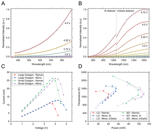
From panels A and B of Figure 2 it can be seen that the intensity of the collected radiance increases with bias voltage, while the peak in emission shifts to within the spectral range measured by the monochromator, both indicative of increasing temperatures and a Joule based heating mechanism. The overlaid lines detailing the result of fitting to Planck's law meanwhile closely match the broad spectra, suggesting the devices are well characterized as a grey-body. Such behavior is in sharp contrast to hotplate emitters fabricated from multi-layered, semi-transparent materials in which oscillations are superimposed onto the emitted spectrum as a result of interferometry within the radiator element itself or the underlying trench of suspended type structures:[7, 26, 32] often necessitating micro-scale patterning or the deposition of metal oxide/carbon containing coatings to ensure a grey-body like response.[4, 6, 8, 33, 34] In the present case however, the combined effects of boron-acceptor absorption and surface-roughness scattering appear sufficient to produce a relatively constant emissivity over the respective spectral ranges measured.[30, 35-37] Correlation of thermocouple derived temperatures with IR radiometer measurements for similar magnitude thickness boron-doped polycrystalline diamond films has previously suggested an emissivity of 0.63, far in excess of the near-zero value expected for intrinsic single crystal diamond.[32, 38]
Panel C shows the current through the hotplate increases monotonically with voltage for low biases, with the difference in low-bias gradient between the two groupings commensurate with the increase in arm length, and hence electrical resistance, from 30 µm to 80 µm. Despite the B/C feed gas ratio lying within the range expected to yield metallic-like transport, slight, non-permanent increases in the gradients can initially be observed up to a bias of ≈3.5 V indicative of a reduction in resistance. Similar reports of such behavior have tentatively ascribed the reduction to the presence of potential barriers within the grain boundaries of polycrystalline films.[30, 39, 40] Upon exceeding ≈3.5 V the current through the devices rapidly drops shortly before failure.
Panel D then plots the temperatures extracted from the spectra captured with the Si and InGaAs monochromator detectors and the Raman system against the applied power. Due to the spectral range of the InGaAs detector extending into the near-infrared, emission from the hotplates is first detected upon exceeding temperatures of ≈600 K. From this point the InGaAs detector indicated temperature continually rises as the applied power increases for both the large and small hotplates, with the gradient gradually falling as the radiative loss becomes non-negligible.[3, 41, 42] After reaching indicated temperatures of 1400 to 1600 K the applied power then plateaus at ≈55 mW and ≈110 mW for the small and large hotplates, respectively, before subsequently dropping until reaching a maximum temperature of ≈1800 K. These trends are then mirrored with the temperatures extracted from the Si detector, albeit at consistently lower values of ≈100 K and a higher onset temperature as a result of the shorter wavelengths measured. Finally, the Raman-system obtained temperatures can be seen to correlate well with those obtained with the monochromator, despite the narrower spectral range covered, with the large hotplate trace diverging from the monochromator traces at 1300 K, and the small hotplate surpassing the performance of its counterpart by reaching an indicated temperature of 2213 K at 49 mW. This temperature greatly exceeds those reached by both conventional multi-layer hotplate structures and existing bulk-like single material devices detailed previously without a corresponding increase in applied power, demonstrating the potential of the geometries used and the PCD material from which the devices are fabricated.
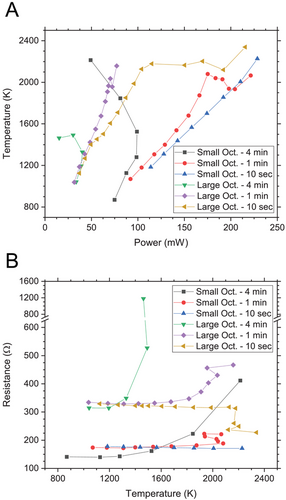
With the temperature values extracted from the narrower spectral width Raman measurements corroborated by those undertaken with the broader range monochromator, the Raman system was used for the remainder of temperature measurements. The spectrometer based system was then used to study a set of large and small octagonal hotplates while being subjected to scans with bias durations of 1 min and 10 sec. The resulting temperature versus applied power and resistance versus temperature traces are plotted in Panels A and B, respectively, of Figure 3 along with the 4 min bias hold scans detailed previously. As visible from panel A, shortening the hold duration results in the peak in applied power described previously being replaced by a gradually increasing gradient with applied power for the 1 min bias hold sample, then an almost linear increase in temperature until ≈2100 K for the 10 sec samples. Meanwhile, from panel B it can be seen that the initial reduction in resistance gives way to a rapidly increasing resistance at elevated temperatures for the 4 min bias hold samples, consistently reaching a minimum at 1100 to 1200 K despite the almost three-fold difference in applied power between the small and large octagon traces. As the bias duration reduces, the temperature at which the minimum resistance occurs shifts to higher temperatures of ≈1300 K for the 1 min hold hotplates, before coinciding with the maximum operating temperature for the 10 sec devices. A sharp decrease in this resistance is then observed for the large octagonal hotplate before a slight increase in temperature to a final value of 2339 K.
2.2.2 Square Hotplates
A series of two- and four-armed square hotplates were then similarly subjected to bias holds of 1 min and 10 sec, with the resulting temperature versus applied power and resistance versus temperature traces shown within panels A and B of Figure 4, respectively. Where multiple devices of each type were studied the additional traces that result are represented by dotted and dashed lines. In a similar fashion to the 1 min and 10 sec bias holds of the octagonal hotplates, both types of square hotplate repeatably show a steadily increasing temperature with applied power until indicated values of 2000 to 2200 K. While the devices tested with a 1 min bias hold fail to reach temperatures above this point, the indicated temperatures of the 10 sec bias hold devices momentarily fall before rapidly increasing to values of up to 2731 K. This surpasses the temperatures achieved with the octagonal hotplates, further exceeding values previously reported for bulk-like hotplates within the literature and setting a new yardstick in performance for ultra-high-temperature micro-hotplates. From the power consumed prior to this reduction it can be seen that the four-armed variant takes slightly less than double the power of the two-armed hotplates to reach temperatures of 2200 K. Given the radiator elements of the respective designs are identical, this shortfall is likely representative of the radiative power emitted from the device. Panel B meanwhile reiterates the shifting of resistance minimum to higher temperatures upon decreasing the bias hold, and the drastic drop upon reaching temperatures of 2200 K for the shortest hold duration devices seen earlier.
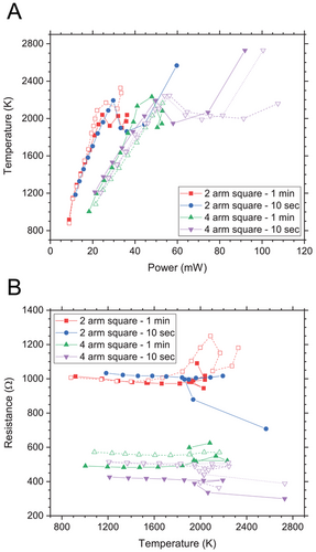
To the first order, the total power required for each design to reach a set temperature will be equal to the summation of the heat lost from conduction through the supporting arms and that emitted radiatively, with each mechanism possessing a different temperature dependancy (∝T for conductive loss and ∝T4 for radiative loss).[1] Fitting the power versus temperature curves for the square devices tested at a bias duration of 10 sec within Figure 4 and using the linear fitting coefficient then suggests a thermal conductivity value at ambient temperatures of 90 Wm−1K−1 to 101 Wm−1K−1 for the boron-doped diamond, with the range in value likely a result of thickness non-uniformities across the set of devices characterized.[3, 43-45] Given heat is generated along the length of the supporting arms rather than atop/within the central radiating element however, the effective arm length responsible for isolation is likely shorter and the extracted value of thermal conductivity overestimated. Nevertheless, this tentative estimate is in-line with thermal conductivities reported within the literature for heavily boron-doped microcrystalline films of similar thickness;[38, 40, 46] defects situated within polycrystalline grain boundaries[47-49] and the presence of boron impurities[46, 50] have both been shown to lead to scattering of the phonons responsible for thermal conduction and a significant decrease in thermal conductivity from the 2200 Wm−1K−1 value observed for high-quality type IIa single crystal diamond. This figure is also well in excess of thermal conductivity values reported for the more commonly used structural materials SiO2 and Si3N4, and approximately half the value reported for Si – the latter of which is often used as a heat-spreading island below the central radiating element of conventional hotplate designs.[2, 21] The absolute power consumption is meanwhile similar in magnitude to that required by suspended type devices to reach up to ≈1000 K.[2] In a compromise between two extremes, the thermal conductivity of the PCD used within is thus able to provide uniform thermalization of the hotplate while ensuring the power consumption is kept to tolerable levels.
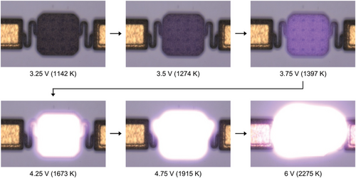
A selection of images captured with the Raman microscope during the 1 min bias hold ramp of a two-armed square hotplate illustrating this compromise are shown within Figure 5. As shown by the visible spectrum micrographs, a uniform faint glow is first visible upon reaching a temperature of 1274 K. This uniformity is in sharp contrast to microscope images taken of meander-based hotplate structures, where the low thermal conductivity of the dielectric layer often results in significant non-uniform temperature measurements.[11, 12] Emission in the visible is also restricted to the radiator element itself and adjoining <50% of the supporting arm, suggesting the temperature along the length of the tether is rapidly reduced before reaching the multi-layer anchor support, preventing the formation of any significant levels of CTE-induced stress. Further increases in temperature result in the emission becoming brighter and completely shrouding the device beneath once exceeding 1673 K as a result of the T4 Stefan-Boltzmann scaling of the radiated power and color shift owing to the temperature dependence of Wien's law.
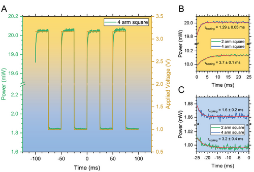
To characterize the thermal response times, a set of two- and four-armed square hotplates were subjected to a 20 Hz, 50% duty-cycle square wave voltage bias and the resulting transient current measured. Temperature-dependant changes in the resistivity will lead to a settling time in the resulting current, and hence applied power, as the device thermally equalises upon changing of the applied voltage, allowing extraction of the heating and cooling time constants. The applied voltages were chosen to ensure the power delivered alternated between ≈1 and ≈10 mW for the two-armed hotplate, and ≈2 and ≈20 mW for the four-armed version; both expected to result in maximum temperatures of 1050 to 1100 K based upon the results within Figure 4. Panel A of Figure 6 shows the resulting power trace obtained for the four-armed device, while panels B and C show example higher-resolution traces of the heating and cooling responses for the two- and four-armed hotplates, with the red lines detailing the result of fitting to the exponential thermal response expected.[2] Averaging over four cycles, the extracted heating and cooling time constants for the two-armed hotplate are 3.5 ± 0.2 msec and 3.6 ± 0.8 msec, respectively, and 1.4 ± 0.1 msec and 1.4 ± 0.4 msec for the four-armed variant. As to be expected with the halving of the thermal resistance that comes with doubling the number of supporting arms, the four-armed geometry takes less than half as long to equalise in temperature as the two-armed design at the cost of increased power consumption.[2] These time constants are an order of magnitude less than the larger, high thermal capacity membrane devices typically used to reach temperatures up to 1600 K, and rival the lowest values reported for faster responding sub-900 K operating suspended type devices as a result of the high thermal conductivity of the boron-doped PCD.[1-3, 12, 13]
To deduce the lifetime of the devices finally, a group of two- and four-armed square hotplates were subjected to bias holds at voltages corresponding to initial applied powers of ≈10 and ≈20 mW respectively until failure. A further two-armed square hotplate was subjected to a reduced bias hold corresponding to an initial applied power of ≈5 mW, which while out of the range of temperatures measurable with either optical setup, is believed to result in temperatures of 670 to 700 K based on extrapolation of the results within Figure 4. The resulting lifetime of the two-armed device tested at ≈5 mW was in excess of seven days with deviations in applied power of <0.5%, while the lifetime of two- and four-armed devices tested at ≈10 and ≈20 mW were of the order of an hour, in accordance with the non-linear trends in device performance with increasing operating temperature observed for conventional multi-layer hotplates.[3]
2.3 Raman Spectroscopy
To investigate the changes in resistance and power consumption upon heating, a two-armed square hotplate was subjected to a 10 sec bias hold ramp with the applied bias turned off between each increment to allow characterisation with Raman spectroscopy. Resulting pertinent spectra are shown within Figure 7 with the temperature reached during each hold point shown to the right. As visible from the ‘pre-test’ trace at the bottom of the plot, the device initially exhibited a Raman spectrum that is characteristic of heavily boron-doped films with broad peaks related to distortion of the lattice by the incorporated boron centered at 465, 1000, and 1210 cm−1. The first of these peaks is widely ascribed to formation of boron–boron dimers, while the latter two correspond to features in diamond's one phonon density of states and appear as a result of relaxation of the wave vector selection rule inherent to Raman scattering.[51-55] Forming a shoulder on the 1210 cm−1 peak meanwhile is the down-shifted zone centre optical phonon (ZCP) of diamond at 1300 cm−1, possessing an asymmetric Fano line-shape as a result of interference between the discrete scattering of the one phonon line and continuum scattering from electronic excitations within the valence band.[56-58] Based on the position of the dimer and ZCP peaks, the boron content within the PCD can be confirmed to exceed a boron concentration of 1021 cm−3 and the threshold for metallic-like behavior.[59]
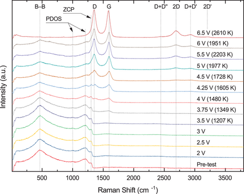
Upon applying power to the device there is little change in the subsequent Raman spectra up to a bias of 3.5 V and an indicated temperature of 1349 K. After this point two peaks indicative of graphitization simultaneously appear at 1350 and 1595 cm−1 and are denoted as D and G within Figure 7, respectively. The D peak is due to the breathing mode of aromatic sp2 rings, while the higher Raman-shift G peak represents the convolution of the D′ peak at 1620 cm−1 and the first-order E2g modes arising from the in-plane bond stretching of pairs of sp2 atoms and rigid layer displacements at 1575 cm−1.[60, 61] With the cross section of graphite reported to be 55 to 75 times higher than that of diamond at an excitation wavelength of 514 nm, the intensity of these bands suggest that at this point the newly formed non-sp3 material constitutes <1% of the composition of the hotplate.[62, 63]
As the bias and temperature continue to rise, the D and G peaks grow in intensity with respect to those associated with the boron-doped diamond until a bias of 5 V and an indicated temperature of 1977 K. In addition, a set of four smaller and broader peaks at 2445, 2695, 2930, and 3205 cm−1 appear representing the overtone and combination peaks of D + D″, 2D, D + D′, and 2D′, respectively.[62, 64] Typically weak in 3D amorphous carbon, the ability to resolve four separate components within this modulated bump suggests a considerable presence of disordered sp2 hybridization within the non-diamond material present.[65, 66] Further increases in bias result in the rise in intensity of the D and G peaks, before briefly halting as the temperature begins to plateau in a similar fashion to that seen within Figure 4A. The features associated with boron-doped diamond are then almost entirely eradicated after increasing in temperature to an indicated 2610 K at 6.5 V, suggesting the sample surface is uniformly covered by a layer of sp2 material with a thickness that exceeds the ≈40 nm penetration depth of the laser.[63] Concurrent down-shifts in the combined G band position to 1585 cm−1 and an increase in the intensity of the 2D peak with respect to the remainder of the second order features and the combined G band peak are also visible within the spectrum, tentatively suggesting an increase in ordering within graphitic planes.[61, 67] The lack of clear doublet and ability to fit both the D and 2D peaks within this final spectra with single lorentzian line-shapes meanwhile suggest that the c-axis ordering between the planes remains poor and reminiscent of turbostratic graphite.[61, 68, 69]
While diamond is metastable at room temperatures and pressures, heating polycrystalline films of the order of 1 mm thick to temperatures beyond 1600 K under vacuum has been shown to result in steady graphitization to more thermodynamically favored forms of carbon.[70-73] Hydrogen terminated sp3 material present within grain boundaries is believed to form long-chain hydrocarbon polymers at 1800 to 2000 K, before C–H bond rupturing facilitates transformation to highly compressed sp2 hybridized amorphous carbon, turbostratic carbon, and nanocrystalline graphite at 2100 K.[71-74] Concurrent graphitization, albeit to a lesser extent than that within grain boundaries, has meanwhile been shown to occur atop crystallite surfaces upon exceeding a temperature of 1700 K, with differing mechanisms either side of the Debye temperature of diamond due to differences in the excited lattice vibration modes; below 2021 K transformation occurs via the breaking of single C–C bonds, while beyond this point conversion is the result of rupturing of multiple C–C bonds, with a corresponding 2.4 fold increase in the associated activation energy.[75, 76] As temperatures surpass 2200 K the graphitization process continues until the initial grain boundary is completely filled with more ordered material, before rapid transformation of grain cores from surrounding grain boundaries and crystallite surfaces. For ≈5 nm diameter dispersed nano-diamond particles in which the surface to volume ratio is greatly increased, lower activation energies result in the onset of this graphitization occurring at temperatures as low as 900 K.[63, 77]
3 Discussion
The behavior observed for the devices presented is thus in accordance with the trajectory detailed within Section 2.3, suggesting the structural changes seen are due to cumulative graphitization of the diamond content within the hotplates. SEM imaging of devices post-test exhibits volumetric expansion and curling of the radiator element in support of such a transformation to less densely hybridized carbon (Figure S1, Supporting Information). The onset of detectable transformation of the ≈1.5 µm thick hotplates meanwhile lies between these reported values for 1 mm thick PCD and nano-diamond particles as a result of the scaling of the surface to volume ratio inherent to van der Drift type growth. The rising resistance upon exceeding temperatures of 1200 K exhibited by the 1 min and 4 min bias hold samples is thus likely a result of the growing grain-boundary content and a corresponding increase in the number of inter-grain potential barriers.[39] For the shorter 10 sec hold duration samples the cumulative exposure to elevated temperatures is reduced, minimizing the amount of graphitization sustained at each hold point and allowing the samples to exhibit a temperature-activated conductivity until reaching 2200 K. As visible within Figures 3A and 4A, and previously detailed, the resulting temperature then briefly drops and plateaus for the majority of the 10 sec ramp rate devices. While it is difficult to fully ascertain the reason for this with heat loss occurring through multiple pathways, graphite has the potential to exceed the thermal conductivity values extracted earlier dependant on orientation and lead to enhanced heat loss through the supporting arms; possess a specific heat that is suspected to be marginally greater than that of diamond at temperatures exceeding 1000 K; and exhibit an emissivity that has the potential to exceed that detailed previously for diamond, resulting in an increase in radiated power.[78-81] The volumetric expansion detailed previously would also likely cause an increase in the emission area and further the power lost radiatively. Shortly after this point, the resistance of the devices falls significantly before device failure occurs at temperatures of up to 2731 K. Considering both doped and intrinsic sp2 hybridized carbon films have shown conductivities within the range 102 Ω−1cm−1 to 104 Ω−1cm−1, this reduction is likely a result of conversion to more ordered sp2 material.[65, 82, 83] Such a supposition is supported by the Raman measurements, with annealing-induced expulsion of boron, ordering of graphitic sheets, and relaxation of compressive stress within sp2 hybridized carbons all shown to yield modifications to Raman spectra similar to that observed between the two final traces within Figure 7.[62, 66, 84-88]
Post-failure imaging of devices tested through incrementally raising the bias voltage exhibit discontinuities at non-repeatable points along the length of the supporting arms (Panels A and B of Figure S1, Supporting Information), likely in part a result of stress arising from the significant warping of the device upon more extensive graphitization and the granular variability within the material that constitute the 3 µm wide arms. Such expansion and movement of the hotplate structure raises the potential for moving MEMS devices based upon reordering of the structural material used. Devices tested with a fixed voltage hold meanwhile demonstrate significant thinning of the radiator elements (Panels C and D of Figure S1, Supporting Information), despite the aforementioned expected increase in volume expected upon conversion to less dense forms of carbon. Based on the vapor pressure of graphite and the pressures maintained during device testing, sublimation would only be expected to occur upon exceeding temperatures of ≈2500 K, far beyond the 1050 to 1100 K temperatures expected for the ≈10 and ≈20 mW biases applied to the two- and four-armed hotplates, respectively.[89] Material loss is therefore likely a result of etching by residual species within the vacuum chamber, with the temperatures similar to the 800 to 1100 K threshold previously observed for etching of diamond within air or oxygen at reduced and atmospheric pressure.[90, 91] Failure of these devices was meanwhile the result of the formation of discontinuities within the radiator element, largely at the junction between the grounded supporting arm and the central radiating element. Such behavior is postulated to be due to asymmetric Thomson heating in which the movement of charge carrying holes results in heat convection and a corresponding shift in the point of maximum temperature toward the grounded electrode, locally accelerating the etching observed.[92] Within microscopy applications the devices are likely to be operated under UHV conditions, while for applications that preclude the use of a continually pumped vacuum chamber the device can be hermetically packaged under UHV conditions with incorporated passive getters, potentially prolonging lifetimes beyond that seen at the ⩽ 5 × 10⁻⁴ mbar pressures used for the current tests.[93]
4 Conclusion
A series of freestanding micro-hotplate structures of varying geometry have been fabricated from a single layer of boron-doped PCD, with Joule heating occurring along the length of constrictive supporting arms in a departure from conventionally used multi-layer structures. Upon steady-state biasing under high vacuum conditions the resulting devices exhibit grey-body like emission within the 475 to 1700 nm spectral range measured, while fitting to Planck's law indicates temperatures of up to 2731 K are reachable at powers of ⩽100 mW; vastly exceeding the 1600 K upper limits of conventional multi-material hotplate structures and setting a new benchmark for micro-hotplate operating temperatures. Characterization of the thermalization time and lifetime of the devices demonstrate rapid millisecond response times, an order of magnitude less than membrane structures capable of reaching up to 1600 K, and lifetimes highly dependant on the ultimate temperatures reached. These trends in device performance and behavior were then correlated with cumulative graphitization and subsequent ordering of the resulting sp2 hybridized material upon exceeding temperatures of 1000 K through the use of Raman spectroscopy. The devices presented have thus demonstrated the potential for single-layer hotplate geometries in reaching ultra-high temperatures, paving the way for next-generation diamond and carbon-based micro-hotplate devices.
5 Experimental Section
The devices presented within were fabricated atop a 12 by 12 mm silicon-on-insulator substrate through the use of Bosch etching, conformal chemical vapor deposition of a ≈1.5 µm thick layer of heavily boron-doped diamond, and subsequent processing with standard micro-fabrication techniques. A full description and accompanying schematic of the process used can be found within the Supporting Information.
In readiness for testing, individual dies were mounted and wire-bonded within open-topped 16 pin DIP packages. The packages were then placed in a custom-built vacuum chamber equipped with a 0.4 mm thick sapphire window and electrical feedthroughs, before evacuating to pressures ⩽ 5 × 10⁻⁴ mbar. During steady-state characterization, voltage biasing and current monitoring was performed with a Keithley 2450-EC source measure unit. A Horiba LabRAM HR Evolution Raman spectrometer equipped with a SynapsePlus Back Illuminated Deep Depletion CCD and 50x objective was used for both Raman spectroscopy at an excitation wavelength of 473 nm, and measurement of the emitted thermal radiation spectrum through blanking the excitation laser. A 600 grmm-1 grating was used while performing Raman measurements to optimize spectral resolution, while a 300 grmm-1 grating was used during thermal emission characterization to allow a coverage of -230 cm−1 to 3810 cm−1 (468–577 nm) in a single scan. The intensity response of the Raman system was characterized before leaving the manufacturer with a calibrated white light source, while the wavelength was calibrated prior to each set of measurements through use of the silicon F1g peak at 520 cm−1.
Broader spectrum scans of the black-body emission was captured with a Bentham TMS300 monochromator fitted with a DH_Si silicon photodiode for measurements from 500 to 1100 nm, and a DH_IGA indium–gallium arsenide photodiode for measurements up to 1700 nm. The intensity correction required for the monochromator system was calculated through the measurement of an Oriel 63358 45 W quartz tungsten halogen lamp of known emission, with the vacuum chamber lid placed in between the lamp and monochromator to account for wavelength-dependent attenuation of the sapphire window. The wavelength correction required was meanwhile determined using the emission lines of a mercury-vapor lamp.
To characterize the thermal equalization time of the hotplates finally, the transient electrical response was determined through applying a square wave voltage to the devices with a GW Instek AFG-2005 waveform generator. The resulting differential voltage across an in-series 1 Ω shunt resistor was then measured with an INA293 current sense amplifier and an Agilent DSO7014A oscilloscope, allowing determination of the current passing through the hotplates.
Acknowledgements
This work was supported by funding from the Engineering and Physical Sciences Research Council under the “Making a Miniature Sun” research grant (EP/V048295/1). [Correction added on January 24, 2024, after first online publication: Figure 3 has been updated.]
Conflict of Interest
The authors declare no conflict of interest.
Open Research
Data Availability Statement
The data that support the findings of this study are openly available in Cardiff University Research Portal at https://doi.org/10.17035/d.2023.0256773783, reference number 256773783.


