Catastrophic Optical Damage in Semiconductor Lasers: Physics and New Results on InGaN High-Power Diode Lasers
Abstract
Among the limitations known from semiconductor lasers, catastrophic optical damage (COD) is perhaps the most spectacular power-limiting mechanism. Here, absorption and temperature build up in a positive feedback loop that eventually leads to material destruction. Thus, this is truly an ultimate mechanism, and its continued suppression is a manifestation of progress in device design and manufacturing. After an overview of the current state of knowledge, new investigations of COD using artificially micrometer-sized starting points created within the active zone in the cavity of 450 nm GaN semiconductor lasers are reported on. Defect growth mechanisms and characteristics are studied during 800 ns current pulses. The defect growth follows the highest light intensity. Secondary defect patterns are studied: complete destruction of the active zone and generation of a point defect cloud at least ≈10 μm into the remaining surrounding material. Extremely large angles (>90°) of damage growth are traced back to the material properties and the aging scenario. The results are compared with former experiments with GaAs-based lasers.
1 Introduction
These days, semiconductor lasers are the most important sources of photonic energy for an immense number of applications in which they are, quasi, at the beginning of a chain of components. Therefore, it is particularly important to know what the reliability of a given semiconductor laser is under certain working conditions. It is therefore a matter of obtaining something like a reliable lifetime prediction. In many cases, such a prediction is achievable by conducting lifetime statistics based on accelerated aging measurements.[ 1 ] In some cases, however, especially in the development of new devices, it is additionally desirable to identify and understand separately the individual degradation mechanisms which in their sum determine the overall lifetime, to be able to eliminate them afterward in a knowledge-based manner.
Catastrophic optical damage (COD) is one of these mechanisms. It occurs particularly in high-power operation of diode lasers, mainly edge emitters, and often manifests itself in spectacular, often macroscopic, damage patterns. In the past, for GaAs-based devices, these mostly occurred at the laser facets, mainly at the front facet. However, this situation has changed significantly with the improvement of coating and passivation technologies for the facets.[ 2 ] Therefore, damage signatures,[ 3-13 ] originally typical of front-facet COD, are also observed in the bulk on such devices, especially after failure at high-emission power levels, at the latest after preparative opening of the device in question. This form of COD is sometimes referred to as catastrophic optical bulk damage (COBD).[ 14-17 ] However, the nature of the effect is always the same, whether it occurs at the facet or in the volume.
The COD is characterized by a very rapid drop in light output intensity caused by a fast “feedback loop.” This feedback loop includes increased absorption and associated heating, which again increases absorption. This leads to a fast temperature rise, which results in a macroscopic defect that eventually suppresses lasing. The phenomenon originates in a tiny region of the active zone of the laser in which the temperature or the absorption are initially slightly increased, but enough to start the feedback loop, which sometimes is called the “thermal runaway.” The reasons for locally increased absorption or elevated temperatures at microscopic “weak” points, which then serve as COD seeds, can be manifold, as discussed, for example, in other studies.[ 18, 19 ] In general, one could distinguish between “intrinsic and extrinsic” causes for the buildup of temperature and absorption. A classical intrinsic scenario would be, for example, a slightly increased facet temperature, which causes a local bandgap reduction. This in turn causes increased absorption of laser light and thus a further increase in facet temperature. Extrinsic scenarios see, for example, defects as local absorbers and heating sites, for example, pre-existing defects, defects generated during laser operation, ridge geometry, or facet protection issues. Moreover, strain fields at metallization edges, for example, at stripe contacts, can cause local absorption.[ 20 ] In general, one could even say that any inhomogeneity in the optically active region could potentially be the starting point of the COD, if only the light output is high enough. A COD-generating mechanism that could be ranked between extrinsic and intrinsic nature was described in papers by Souto et al.[ 18, 21 ] It has been explained that under certain conditions in modern quantum-well (QW) structures, such high-temperature gradients in the growth direction could occur such that the limit for elastic deformation of the involved materials could be exceeded and the stress relaxation would be realized by defect generation. These defects would then act then as starting points for the COD process.
We pointed out that the actual COD process, that is, the establishment of the positive feedback loop, is very fast. In a previous review article,[ 13 ] we dealt precisely with these processes and the corresponding time constants. In this context, the term “fast” points to the nanosecond range.[ 22-24 ] This holds for the abrupt temperature rise. What follows then is defect propagation, which is fed by the laser light, or, if lasing is terminated, by spontaneous emission amplified in the remaining gain material. This propagation has been directly imaged by Jacob et al.,[ 25 ] and analyzed by Hempel et al.[ 26 ] Typical initial defect propagation velocities are, depending on the optical power density present, 10−50 ms−1 and >100 ms−1 in GaAs- and GaN-based devices, respectively. Although these initial speeds slow down quickly, within a fraction of a second (e.g., 160 μs[ 25 ]), the laser is so damaged that the device fails and the process becomes self-terminated.
For GaAs-based devices, it has been shown that the temperature actually reaches at least the melting point of the material of the optically active region, for example, 1580 °C for Al0.35Ga0.65As[ 27 ]; see also the studies there. Little material is available on this issue for GaN-based devices. However, it seems that already at ≈1000 °C a decomposition of the material starts.[ 28, 29 ] So, it looks like the more stable material under ambient conditions, the GaN, becomes unstable as the temperature increases toward ≈1000 °C. Please note that temperatures in the context of damage in the semiconductor always depend on several factors. These are the damage limit (e.g., generation of point defects), the temperature-dependent shift of the optical properties of the different materials, and the efficiency (wall plug efficiency) of the lasers. Although the temperatures themselves are not directly comparable, there is the connection that the high light intensity in the cavity of a semiconductor laser is able to transfer energy very quickly to local absorption foci and generate a temperature by absorption in nanoseconds that completely destroys the material. It should also be mentioned that the high-energy short-wavelength radiation of GaN-based diode lasers, especially in the UV range, can also trigger chemical reactions at the facet that lead to degeneration.[ 30 ]
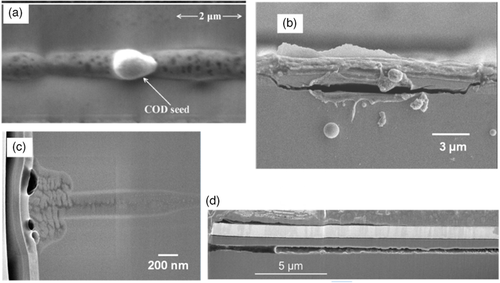
Figure 1 shows the differences in COD signatures in GaAs-based (Figure 1a,c) and GaN-based (Figure 1b,d) material. While in GaAs diode lasers a swelling out of material at the facet is typical, the COD in GaN diode lasers leaves holes and gaps. Internally (cross-sectional images in Figure 1c,d), a region of solidified melt is found in the GaAs-based device, while in GaN, a cavity is formed along the waveguide (WG) by the COD.
Throughout the history of research on COD, the question of whether COD is not also (partially) controlled by the current flow through the diode has also played some role.[ 31 ] This idea is also very obvious in that the electrical resistance of GaAs decreases to 1/26 at the solid−liquid phase transition.[ 32 ] Thus, melted regions represent effective current paths. A recent paper by Adams et al.,[ 33 ] uses device modeling to distinguish between heat sources on GaAs-based devices. It was found that taking into account the influence of the operating current gives better agreement with their COD observations.
In what practical situations does a researcher or user of diode lasers observe the COD? 1) The COD process can start when the power of a diode laser is ramped up by increasing the DC operation current. The onset point is sometimes called the COD threshold. However, in such an experiment, the laser may heat up to such an amount that it decreases its power to such an extent that it is no longer sufficient to cause the COD. This situation is called thermal rollover. 2) Sudden failures can be observed in long-term experiments, for example, in constant current operation. At least in part, such failures could be due to COD. In this situation, the thought is that long-term operation has caused gradual changes, such as the generation of point- or higher-dimensional (extended) defects, which lower the COD threshold to below the actual power level. 3) Optical feedback on external elements, such as mirrors, has been shown to be a degradation mechanism, leading to COD.[ 34-37 ] This can happen, for example, quite by chance during the optical alignment of a setup. The underlying principle is that the optical feedback lowers the laser threshold and thus increases the power, which can also trigger the COD, especially if the power is close to the COD threshold anyway. Regardless of this way of modifying the laser cavity, additional heating can also occur simply by reflecting the laser light back to the emitting laser.[ 38-40 ] 4) In addition, there are specific experiments in which the COD is intentionally provoked.[ 26, 27, 41-43 ] This can be achieved, for example, with single pulses that generate a laser power that is above the COD threshold. If the pulses are short enough (<μs), the process can be reignited in a possible subsequent pulse and thus stroboscopic resolved in time. It is also possible in COD devices for which this mechanism is actually not relevant.[ 41 ] Such experiments also led to the results presented in this article.
If one utilizes the knowledge gained in the course of many studies with GaAs-based diode lasers about the mechanisms underlying COD, it is now possible to trace back most of the later-observable damage patterns to root causes of the COD,[ 44 ] even if the observed damage pattern is not explained in a trivial manner. As the final damage pattern in GaN devices looks substantially different, these relationships have to be investigated. Up to now, only front-facet COD events in GaN-based diode lasers have been reported.[ 28, 45 ] However, also for GaAs-based devices, the occurrence of COD was first observed at the facets before they were hardened by special passivation procedures. The COD started to occur at times in the cavity, far from the mirror facet, after which the weak point was removed, for example, studied in other works.[ 46-50 ] This will likely happen for GaN-based devices too, once the facet passivation technologies will be improved further. This is one important motivation for the study, whose results are presented in the article. We provide insight into the dynamics of the COD-related defect growth inside the cavity of GaN-based diode lasers. For this purpose, we prepared artificial defects inside the cavity, and COD was triggered in single-pulse excitation experiments. We developed preparation procedures to reveal the defect structure inside GaN-based devices and studied primary and secondary defect patterns.
2 Experimental Section
2.1 GaN-Based Diode Lasers
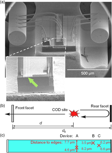
Commercial GaN diode lasers (OSRAM PL TB450B) were analyzed. The epitaxial structure contained an asymmetric QW structure similar to the one described by Strauß et al.[ 51 ] They emitted 1.6 W output power at 1.6 A operation current in the continuous wave mode with a threshold current of 0.2 A. The laser ridge had a dimension of 15 × 1200 μm (width ×length). The front facet was antireflection coated, resulting in ≈5% remaining reflection, whereas the rear facet had a dielectric coating with nearly 100% reflectivity. The emitters were packaged p-side up (ridge up) in TO56 cans; see Figure 2 . The transistor outline-can caps were removed shortly before the experiments. The heat sink temperature of the diode lasers was thermoelectrically stabilized at 25 °C during the COD experiments. Here, we present data from six devices of the same batch with nearly identical optoelectronic characteristics.
2.2 COD Test Procedure of Devices Without Artificial Defects
In these measurements, a single-pulse step test was applied.[ 52 ] A fixed pulse length of 800 ns was used, and the current was increased by 1.0 A for each subsequent pulse (pulse generator: Picolas PLCS-21; current generator: Picolas LDP-V 50-100V3). This was done until a clear COD signature was detected, that is, a sudden drop in emission power detected by a fast photodiode (Thorlabs DET10A/M, rise time: 1 ns). The unambiguous verification of the irreversible damage caused by COD was done by monitoring the optical power supplied by the laser under 0.8-A low current pulse between the individual steps. Such pulses generated almost identical photodiode traces before COD but a pronounced drop in emission power after COD. In addition, a time-synchronized Basler Ace acA1300-30um charge coupled device camera took snapshots from the side of the device, providing a time-integrated spontaneous emission image along the laser axis. The average COD threshold I COD,fresh resulting from these tests was taken as the characteristic value for the entire device batch.
2.3 Generation of Artificial Defects
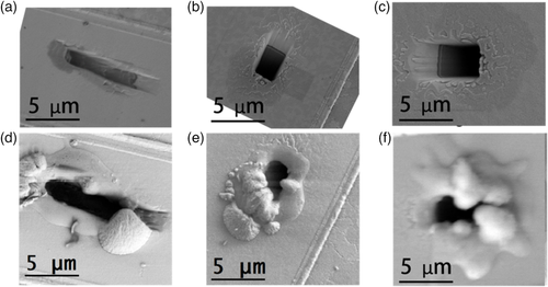
A focused ion beam (FIB; type: FEI Helios NanoLab 600i) was used to cut small trenches of ≈2 × 2 μm in the ridge WG. The cuts were made at the direct incidence of the ion beam. As the diode laser could not be plated with a thin conductive surface, the local charge accumulation during FIB milling resulted in a beam deflection causing a deviation from the intended quadratic shape. Figure 3a–c shows typical electron microscopy images (SEM) of such defects. The depth of the trenches varied due to the beam drift, but in any case, it penetrated the epitaxial structure including the entire WG (including the QW). The first defect (device A) was located 800 μm from the front facet. The amount of integrated light between this defect location and the front facet compared with the amount of light between the defect and the rear facet was almost equal, see sketch in Figure 2b. To identify this point, the intracavity light intensity in the rear section was estimated to be two times the value per length compared with the front section, caused by the coatings on rear and front facets. This led to a value of 2/3 of the length measured from the front facet. Therefore, the artificial defect in device A was placed at a distance of 800 μm from the front facet, shown in Figure 3a. The second (device B, Figure 3b) and third (device C, Figure 3c) artificial defects were located 990 and 1060 μm from the front facet, respectively. An overview of the FIB defect positions along the ridge is given in Figure 2c. Thus, all artificial defects were located in the rear region where impinging light intensity from the front part was expected to be stronger than the light impinging from the rear facet. Note that the phrase impinging light intensity is intended to explicitly highlight that the light generated via laser transition enables rapid energy redistribution in the diode laser cavity itself. Therefore, it is not so much a question of where exactly the photons are generated in front of or behind the artificial defect in the cavity but where they are absorbed. The position of the defects with respect to the middle of the 15 μm wide stripe varies slightly, as shown in Figure 3c. The artificial defect of device C was in the middle of the ridge, whereas those of devices A and B were slightly off-center.
2.4 Inspection of the Defect Structures
Secondary electron microscopy (SEM) and cathodoluminescence (CL) images were recorded with a Zeiss LEO field-effect SEM, which had an attached CL apparatus (Gatan MonoCL 2). CL measurements were done at 80 K, to improve the signal/noise ratio. Panchromatic CL images and local spectra were recorded.
2.5 Etch Preparation
To investigate the COD-related damage in the diode laser, the top contact metal layer was removed by wet etching. The gain area was limited by a blocking dielectric layer beneath the metal layer at both sides of the ridge; this permitted to remove the contact metal layer by under etching the dielectric blocking layer, which permitted to lift off the full metal layer. 5% diluted HF was used for wet etching. The process was stopped every 2 min, and the laser was rinsed in deionized water and observed at the microscope to evaluate the state of the contact metal layer after each etch step. This procedure was repeated several times until the metal layer was fully removed without damaging the semiconductor. This took 13−15 min accumulated etching, after which the laser cavities were ready to be studied in the SEM.
3 Results
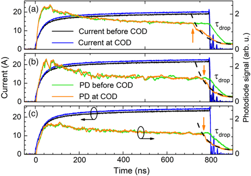
COD thresholds were determined by applying the single-pulse step test to pristine devices. Figure 4 shows three examples of the photodiode traces of the last step before COD and the following 1 A-increased current step, when COD takes place. The onset of the COD is clearly visible and indicated by arrows at a time of t COD in the pulse (Figure 4a: t COD = 644 ns; Figure 4b: 685 ns; Figure 4c: 689 ns). The drop in optical output power was fit by an exponential decay. This allows to extract a power decay time of about 50 ns (individual device characteristic decay times and standard deviations are given in Figure 4). A recording of the spontaneous emission along the laser axis during the event (from the side) and a microscopic inspection of the device verified that all COD events in the reference devices took place at the front facet. The average COD threshold determined from the step tests is I COD,fresh = 20.7 A. The step test on the reference devices revealed a very homogeneous behavior of the device batch, both in the COD threshold current and in the characteristic power drop time during COD; see Figure 4. Therefore, the I COD,fresh value at this pulse length as well as the COD kinetics can be seen as prototypical for these diode lasers.
Next, we subjected the devices with FIB artificial defects to conditions that we suspected would cause COD. On the one hand, we had to avoid the COD at the front facet; on the other hand, the onset of the COD within a single current pulse was desired. That was because we wanted to analyze the very early stages of the COD. Considering the current levels to start COD at reference devices and the localized artificial FIB defects, we adopted the compromise to apply current pulses of I COD,def = 0.8 and·I COD,fresh≈17 A.
Figure 5 gives the current and photodiode traces of these experiments for devices A−C. The COD took place at : t COD ≈200 ns (device A), 90 ns (device B), and 250 ns (device C). The drop in light output intensity caused by the COD was fit with an exponential function, as indicated in Figure 5. The decay times τ drop are significantly longer than those in the initial reference experiments. The values of τ drop increase with the distance to the front facet, from where the photodiode records the emission; see Figure 5d.
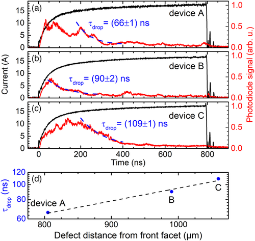
Figure 3d–f shows the trenches cut by the FIB after the COD was triggered. An agglomerated rim of ejected material at the edges of the FIB trenches is clearly visible.
The next step was to reveal the internal defect structure. The top metal layer (p-side) was thick enough to prevent the observation of the laser cavity in CL measurements; the electron beam cannot reach the semiconductor layers and neither, the emitted luminescence can cross the metal layer. Therefore, we proceeded to remove the metal layer, to open the laser cavity for the e-beam, for morphology observation, secondary electron image, and CL analysis in the SEM. Figure 6 shows the revealed damage structure after etching. Obviously, the damage produced by the COD event is located around the trenches, which behave as predamaged areas seeding the degradation process when the single pulse is applied. Figure 7a–c presents panchromatic CL images at specific locations of the pattern observed in the SEM images. The darkest CL contrast is observed in the trenches, which evidences that the COD process starts at the trench. On the other hand, the grooves and ridges revealed by the etching present different contrasts in the CL images, revealing the laser intensity distribution associated with mode filamentation.

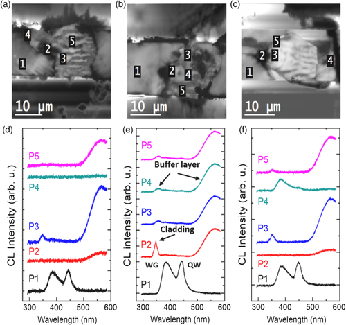
Figure 7d–f shows the results of CL spectral analysis of the damaged regions, as indicated in Figure 7a–c. The spectrum of the undamaged regions, point 1 in each subfigure, exhibits the QW emission (≈440 nm) and the WG layer emission (≈380 nm). Spectra at different positions of the damaged regions were also recorded. The CL peaks associated with the QW and the WG are not observed all over the damaged region, which accounts for the full removal of the WG and QW in the damaged region. The spectrum in the damaged region is dominated by a broad band, corresponding to the yellow luminescence (YL) (≈560 nm) of GaN arising from the GaN buffer layer. The YL is much higher than the intrinsic emission, accounting for the generation of the point defects responsible of the YL during the degradation. The YL band is related to Ga vacancies.[ 53, 54 ] As mentioned before, the active region was empty after damage, thus forming a void.[ 29, 55 ] Therefore, the etching pattern reveals the footprint of the damage after upper layers; cladding and semiconductor layer on top of the void were removed by etching.
The remaining material is mainly the GaN buffer layer, but there are also vestiges of the AlGaN cladding layer in the regions with bright CL contrast in the GaN buffer layer, while the WG and QW fully disappear.
The different CL contrast between the grooves and ridges (the dark and bright stripes visible in the defect region, Figure 7a–c) is analyzed by the local CL spectra. The CL spectrum of a groove with dark contrast only exhibits the YL; meanwhile, the ridges with bright contrast exhibit an intense YL, but also a weak peak at ≈350 nm, corresponding to the AlGaN cladding layer.
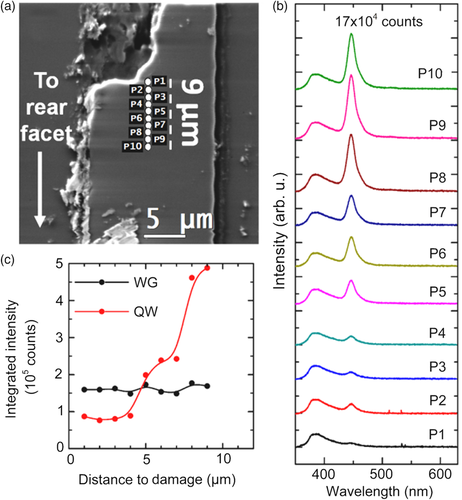
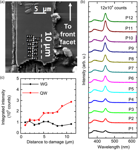
In previous works, it was shown that the boundary between the damaged and undamaged regions was abrupt on a scale <10 nm. In fact, scanning transmission electron microscopy images at the end of the damaged front revealed the well-defined QW structure.[ 29 ] The CL spectrum just beyond the damaged pattern revealed in the SEM and panchromatic CL images, point #4 of device B in Figure 7f, shows effectively the existence of the QW and the WG. However, the emission from the QW is partially quenched, revealing that defects acting as nonradiative recombination centers have been created, which are responsible for the lower CL emission, even if the epitaxial structure is not obviously physically affected. To investigate this transition region between the damaged site and undamaged laser material in detail, additional CL spectra were recorded in this area. Figure 8 and 9a show the equidistantly distributed measuring points along the laser ridge with a spacing of 1 μm using the example of device A toward the rear (Figure 8) and front (Figure 9) facet. Figure 8b and 9b give the spectra at these spots; the peaks arising from the WG and QW are clearly visible. The integrated intensity of these two peaks from Figure 8b is plotted in Figure 8c and 9c. While the WG CL intensity remains nearly unaffected on the same level, the QW CL signal rises significantly over the first 10 μm starting from the rim of the damaged zone in both front and rear directions with respect to the region heavily damaged by COD.
4 Discussion
When comparing the COD scenarios in devices without and with defects, see Figure 4 and 5, we see a striking different behavior. While in Figure 4 all parameters, I COD, t COD, and τ drop, are fairly uniform, Figure 5 shows less uniformity overall. In particular, t COD can be only roughly estimated, while the emission power at t < t COD is very irregular. This is because the data in Figure 4 show, at least until 0 < t < t COD, the emission from pristine lasers, while the data in Figure 5 show the emission of predamaged devices, and this from the beginning, that is, starting at t = 0. Thus, the pronounced power fluctuation at 0 < t < t COD in the damaged device is absolutely not surprising.
- Obviously, the t COD values are smaller in the damaged devices. The step width of 1 A used in the tests carried out with pristine devices makes sure that the actual current that causes COD does not exceed I COD of the particular device by more than 1 A, that is, not by more than ≈5%. In case of the damaged device, we do not know I COD. Testing this would require a number of identically damaged devices. Our choice, I COD, def = 17 A, was probably more than 5% above I COD of the predamaged devices resulting in the smaller t COD values.
- Second, the recording of the emission signal is different for devices with and without defects. In devices without defects, the damage takes place at the front facet, and the signal drop, quantified by τ drop, can be seen as a measure for the growth of the defect. These drop times of ≈50 ns are in the range of the values measured for GaAs-based devices by reflection measurements at the facet of 30 ns in the study by Hempel et al.,[ 43 ] and 26 ns.[ 56 ] In devices with defects, however, where there is actively pumped material between the photodiode and the COD site, the direct relationship between τ drop and defect expansion is impaired, that is, τ drop is lengthened. This is verified by the (exponential) increase in τ drop with the distance, as shown in Figure 5d. So here we see a combined effect that makes it difficult to correlate directly with damage propagation.
Despite these uncertainties, our data allow first estimates about defect propagation during degradation. Taking the τ drop values of ≈50 ns for the pristine devices and assuming the COD seed in center of the 15 μm-wide ridge, we get a lateral defect propagation velocity of 150 m s−1. This estimate almost matches the 110 m s−1 determined by Mura eτ al.[ 55 ] for the longitudinal defect propagation. In contrast, a coincidence of longitudinal and lateral defect emergence speeds indicates isotropy of defect propagation. We will come back to this later when we look at the physical damage patterns. Defect propagation velocity is estimated to be between 70 and 110 m s−1 by considering the time to generate the damage and the final defect size. However, these values may be less reliable due to the effects mentioned in the preceding paragraphs.
It was estimated that the disintegration of GaN can take place at ≈1000 °C,[ 29 ] well below its melting temperature of ≈2500 °C. The material surrounding the FIB trenches after the COD, Figure 3d–f, is mainly gallium, resulting from the decomposition of the WG and QW. It is pushed out by nitrogen vaporization within the active zone of the laser. This is in line with previous results obtained with similar lasers where the COD started at the front mirror and where the ejection of Ga was observed straight through the mirror of the front facet.[ 11, 29, 55 ]
Obviously, the etching process has revealed the parts of the laser structure that were catastrophically damaged during the current pulse; see Figure 6. In fact, what we observe is the footprint (fossil) of the material removed during COD. In contrast to AlGaAs/GaAs lasers,[ 57 ] where the active zone of the laser gets typically molten and recrystallized without any significant mass loss during the COD process,[ 26 ] in GaN lasers, the active region in the damaged part of the laser is empty, that is, not existing anymore. Therefore, the etching removes the top part of the laser structure, the p-side, and the SEM image shows a picture of the remaining material in the n-side of the structure. Note that outside the damaged region the etching only removes the top metal layer, leaving the laser structure completely intact, but rich in point defects close to the damaged area. One can appreciate in the SEM and CL images, Figure 6 and 7, that the artificial defects are the origin of the damage. This is especially conspicuous in the CL image of device C, Figure 7c, where one observes a dark area with a rectangular shape, corresponding to the FIB trench, and the leftovers of a thermal shock front propagating away from it.
The COD growth itself runs toward the front facet, starting from the FIB trench. As shown in the sketch of Figure 2b, the FIB defect positions were placed in the region where the intracavity light intensity hitting the COD site from the front, even under consideration of the asymmetrical mirror reflectivity, is higher than that from the rear. This supports the basic assumption that the energy source for the COD is the amplified light impinging onto the defect. Following the results of earlier papers,[ 44 ] dealing with the reconstruction of COD damage pattern in GaAs devices based on fundamental assumptions, our present data verify that the main driving mechanisms in GaN lasers are actually the same, the energy redistribution via the intracavity light field, the local light absorption, and the ability of the material to spread the heat caused by the absorbed light (by heat conduction). Therefore, the same “reconstruction principles” can help to trace back also the root causes of the COD in GaN-based devices.
In addition, the shape of the damage pattern depends on the lateral position of the FIB trench in the ridge, that is, perpendicular to the laser axis. One observes a symmetric pattern with respect to the central axis along the ridge, in device C, for which the trench was just in the middle of the ridge. The other lasers, for which the trenches deviated from the central axis of the ridge, exhibit asymmetric patterns; see Figure 6a,b. If one looks at device C, one observes around the trench (artificial defect), oriented toward the front facet, semicircular halos, suggesting a shock wave-type singular heating event; then, it is followed by a flame-like structure along the ridge, formed by grooves and ridges parallel to the laser cavity. In contrast, the two other lasers show an asymmetric pattern close to the trench, the semicircular halos are not resolved, but the longitudinal flame-like pattern is also observed. These longitudinal grooves seem to be associated with the filamentation of the optical mode, as previously reported for COD in GaAs-based and single-mode ridge WG structures and GaN-based diode lasers.[ 11, 58 ] The dependence on the position of the trench across the ridge reinforces the hypothesis of the optical mode redistribution in the presence of a hotspot or damaged region in the active zone of the laser. Therefore, the COD damage pattern is governed on each scale by the actual light field distribution during the defect growth. This light field in turn is shaped as well by the growing defect.
The lateral (in-plane) spread of the damage pattern, starting from the FIB-generated defect, shows an opening angle α > 90°, for example, see indicated α in Figure 6c. This value is substantially larger than the values found for GaAs-based devices, which are in the range from 6° for the 980 nm emitting InGaAs laser to 18° for 808 nm AlGaAs diode laser. Even for the 650 nm emitting InGaAlP-based devices, an angle of only 24° was reported.[ 59 ] Following the modeling approach in other studies,[ 44, 59 ] according to which the angle of propagation is determined by the thermal conductivity of the COD-affected material to its surrounding, a much higher thermal resistance between the material already damaged by COD and the undamaged areas is indicated. It is likely a direct consequence of the different processes in both types of lasers, melting and resolidification in the case of GaAs and decomposition and material ejection in GaN lasers. The heat transfer from the gas-filled cave to the undamaged material in GaN-based devices is very weak compared with the one between liquid and solid material in GaAs devices. The poor lateral heat conduction in the GaN device is additionally verified by the CL measurements shown in Figure 7 and 8. The WG remains nearly unaffected at the rim of the damaged region, shown by the constant CL signals in Figure 8c and 9c. In case of the QW, the point defect density, which causes a drop in the QW signal, increases significantly when approaching the heavily damaged zone. This takes place at both sides, toward the rear and front, which suggests that the defects responsible for the reduction of the QW quantum efficiency around the damaged region are created by either the vast temperature gradient or the thermally induced stress, produced locally around the damaged region. However, the extent of this region is limited to ≈10 μm (Figure 8 and 9), whereas for ridge-type GaAs-based devices, after intracavity COD events, a heat-driven point defect growth over a distance of ≈100 μm was reported.[ 60 ] This striking difference results from the large difference in heat transfer between GaN- and GaAs-based materials and the resulting different degradation kinetics.
5 Conclusion
After providing an overview of current research on COD at semiconductor lasers, we present the results of a study on the degradation behavior of 450 nm-emitting GaN-based high-power laser diodes. COD is induced in the devices at artificially generated micrometer-sized defects within the emitter stripe by applying a series of single current pulses. While fresh reference devices show this well-known effect at the front facet, the predamaged devices show the COD within the emitter stripe, whereby the small artificially generated defects are actually the seeds for defect propagation. This scenario is substantiated by a sequence of analytical investigations that also involves a number of preparative technologies, including FIB preparation of artificial defects that act as primary defects; SEM inspection of the defects and their surroundings; etching techniques to unveil the internal defects generated during the COD; and imaging as well as spectrally resolved CL.
The following conclusions are drawn on the bases of the analysis of the secondary damage caused by the COD event that lasts less than 800 ns: 1) The defect growth during the COD takes place in the direction of the highest light intensity within the laser cavity. This is in the actual case of our experiments toward the front mirror. This proves that the direction of the damage propagation is related to the position of the starting point (initial defect) and runs in the direction of the higher incidence of light. 2) The decomposition of the active zone during the COD involves material ejection. 3) We observe two types of secondary defects, the physical destruction (decomposition) of the WG, but also the generation of a point defect cloud reaching at least 10 μm into the apparently undisturbed material around it. 4) The damage patterns within the defect regions suggest that ridges and grooves are due to the light intensity distributions associated with beam filamentation. 5) The unusually large lateral propagation angle of >90° of the damage growth caused by the COD is determined by both material properties and the aging scenario of material decomposition with gas formation.
These results are compared with the results of corresponding experiments with GaAs-based high-power lasers. The findings regarding GaN-based lasers are of particular relevance for the future, as it is expected that in this material system, as in GaAs, with better control of facet technologies, problem areas within the laser cavity, for example, epitaxial defects or damage caused by processing, will play a real important role.
Acknowledgements
S. D. and J. J. were funded by Junta de Castilla y Leon (project VA283P18), and European Fund for Regional Development (FEDER).
Open access funding enabled and organized by Projekt DEAL.
Conflict of Interest
The authors declare no conflict of interest.
Biographies

Martin Hempel received his diploma and Ph.D. in physics from Humboldt University Berlin, Berlin, Germany, in 2009 and 2013, respectively. He worked as a postdoc from 2013 to 2015 at Max-Born-Institute in Berlin, Germany, and from 2015 to 2017 at Paul-Drude-Institute, Berlin, Germany. Since 2017, he has been with the Fraunhofer Institute for Reliability and Microintegration IZM in Berlin. His research interests include photonics, optoelectronics, and applied semiconductor physics. He is a member of the German Physical Society.

Shabnam Dadgostar received her B.S. in physics from Damghan University, Damghan, Iran, in 2002, her M.S. in solid-state physics from Tarbiat-Modares University, Tehran, Iran, in 2006, and her Ph.D. in experimental physics from Humboldt Universität zu Berlin, Berlin, Germany, in 2016. From 2006 to 2011, she was a research assistant with the Institute of Physics, Sharif Technical University, Tehran, Iran. From 2017 to 2018, she was a postdoc researcher at Electronic Research Center, Iran University of Science and Technology, Tehran, Iran. Since 2019, she has been working as a postdoc at GdS-Optronlab, Universidad de Valladolid, Valladolid, Spain. Her research interest includes the growth of semiconductor heterostructures using molecular beam epitaxy, fabrication of micro- or nanostructured surfaces, optoelectronic devices, and study of optical properties of semiconductors and optoelectronic devices.

Juan Jimenez received his B.S. in physics from the University of Valladolid in 1975. From 1976 to 1979, he was with the Universite des Sciences et Techniques du Languedoc (Montpellier-France) as a research student. He received his Ph.D. in physics from the University of Valladolid, in 1979, and Ph.D. in physics from the Universite des Sciences et Techniques du Languedoc in 1981. He was an associate professor in condensed matter physics at the University of Valladolid until 1992, when he was appointed as a full professor in condensed matter physics. His research interest includes the optical properties of semiconductors, for example, the study of laser diode degradation using optical characterization tools, optical characterization of semiconductor nanowires, and optical analysis of solar cells, among others.

Robert Kernke received his B.Sc. in physics from the Freie Universität Berlin, Germany, in 2017. Currently he is working on his M.Sc. thesis. He joined the Max-Born-Institut in 2015 and worked since then in several labs as a research assistant. His main fields of interests are thermal properties of high-power diode lasers based on GaAs and GaN materials. He coauthored eight scientific publications.

Astrid Gollhardt is a technical engineer. From 1989 to 1993, she was a staff member in the Department von Klitzing at the Max Planck Institute for Solid State Research in Stuttgart, Germany. Since 1997, she has been a staff member in the Department of Environmental and Reliability Engineering at the Fraunhofer Institute for Reliability and Microintegration IZM in Berlin, Germany. Her field of activity covers the analysis and testing of micromaterials, using focused ion beam, scanning electron microscopy including energy-dispersive X-ray spectroscopy, atomic force microscopy, and in siτu mechanical and thermal measurements in a scanning electron microscope to characterize defects in electronic components.

Jens W. Tomm received his diploma and Ph.D. in physics from Humboldt University Berlin, Berlin, Germany, in 1982 and 1984, respectively. During 1993–1995, he was with Georgia Tech, Atlanta, GA, USA, in 1999 with Riken, Sendai, Japan, and in 2018 with the East China Normal University, Shanghai, China. He became a member of the scientific staff of the newly founded Max-Born-Institute in 1995. There, he runs the optoelectronic device group. His research interests include photonics, optoelectronics, and applied semiconductor physics. He is a member of the German Physical Society, the E-MRS, and senior member of the Optical Society of America.


