Temperature and illumination dependence of silicon heterojunction solar cells with a wide range of wafer resistivities
Funding information: Australian Renewable Energy Agency, Grant/Award Number: 2017/RND001; Solar Energy Technologies Office, Grant/Award Number: DE-EE0008549; U.S. Department of Energy, PV Foundry, Grant/Award Number: DE-EE0008975
Abstract
Recently, the significant improvements in the surface and contact passivation of silicon (Si) solar cells as well as their bulk quality have shifted their operating point to higher injections. Hence, they are less dependent on wafer doping. This shift opens an opportunity of using high-resistivity wafers for practical photovoltaic applications, introducing a promising approach to push the cell efficiency towards the intrinsic limit and to improve the module reliability by increasing the cell breakdown voltage. Therefore, insights into the performance of Si solar cells using high-resistivity wafers at various operating temperatures are of significant interest. In this study, we investigate the temperature- and illumination-dependent performance of Si heterojunction (SHJ) solar cells using a wide range of wafer resistivities (between 3 and 1000 Ω⋅cm). Although a reduction in the passivation quality of the passivating contacts is observed at elevated temperature, the impact on the temperature coefficient of the open-circuit voltage (TCVoc)—the dominant contributor to the temperature coefficient (TC) of the cell efficiency—is very limited. Their TCVoc are still dominated by the temperature dependence of the effective intrinsic carrier concentration. Furthermore, we also find that the investigated cells are more sensitive to temperature variation at lower illumination intensities. It is noteworthy that the efficiency of the cells fabricated using high-resistivity wafers is comparable to that of the reference cells at any given temperature, highlighting the potential of using high-resistivity wafers for solar cells.
1 INTRODUCTION
It is well known that the fundamental limit of silicon (Si) solar cells, as an indirect bandgap material, is defined by the Auger recombination.1, 2 In principle, this recombination can be reduced by using high-resistivity (low doped) wafers.1, 2 However, due to the compromise between the doping density and excess carrier concentration (Δn) [or effective lifetime (τeff)] at the maximum power point,3 Si wafers with bulk resistivities below 10 Ω⋅cm are usually used for commercial solar cells.4, 5 This compromise can be relaxed if both the bulk quality and the surface and contacts passivation are significantly improved.
Recently, significant improvements in the quality of the passivating contacts, used to reduce the recombination at the Si-metal interfaces, have been reported.6-10 Solar cells that integrate these contacts such as Si heterojunction (SHJ),11, 12 interdigitated back contact,6, 13 polycrystalline Si on oxide (POLO),7 tunnel oxide passivated contact (TOPCon)8, 14 and transition-metal-oxide-based cells9, 10 exhibit high open-circuit voltages (Voc) above 720 mV due to high quality passivation of both surfaces and contacts as indicated by extremely low surface saturation current densities (J0s)15 below 10 fA/cm2. These cell structures also benefit from the high bulk lifetime (τbulk) of commercially n-type Czochralski (Cz) substrates. Nowadays, ingot manufacturers often deliver τbulk above 3 ms across the entire ingot,16 with the top parts reaching τbulk of 15 ms.17 High τbulk coupled with excellent surface and contact passivation can push those solar cell operating points to the high injection regime at which Δn is usually at the order of 1015 cm−3.18, 19 In this case, for high-resistivity wafers, their effective bulk resistivity (the bulk resistivity under the operating conditions) is significantly lower than their dark bulk resistivity as the former is defined by Δn at the high injection regime, which is remarkably higher than the doping density. Therefore, it is expected that the detrimental impacts on the fill factor (FF) under the operating conditions when using high-resistivity wafers for Si solar cells are no longer an issue. Hence, the above solar cell architectures may benefit from using wafers with higher bulk resistivities.18, 19
Studies of solar cells fabricated using high bulk resistivity substrates (>10 Ω⋅cm), beyond the commercial resistivity range, are very limited. Glunz et al.20 investigated the efficiencies of TOPCon cells as a function of bulk resistivity (up to 100 Ω⋅cm) using modelling. The simulations revealed that cell performance is independent of the bulk resistivity in the range of 5–100 Ω⋅cm. Jay et al.19 reported that the efficiencies of SHJ solar cells with bulk resistivities in the range of 5–10 Ω⋅cm are similar to those of cells fabricated using 367-Ω⋅cm wafers. Simulated efficiencies of other industrially relevant cell structures with bulk resistivities in the range of 10–100 Ω⋅cm are shown to be comparable to those cells that use 1–10 Ω⋅cm wafers when the Shockley–Read–Hall (SRH) lifetimes (τSRH) of 1 and 10 ms are assumed as the dominate bulk recombination.21 For cells fabricated on wafers with even higher resistivity (>500 Ω⋅cm), it has been shown by simulations that they can outperform cells made on standard wafers (<10 Ω⋅cm) if their τSRH is in the millisecond range.22 This offers a great opportunity to significantly reduce the Auger recombination and hence, to push the cell efficiency of current technologies closer to the maximum theoretical efficiency. Furthermore, using high-resistivity wafers can improve the module reliability by increasing the cell breakdown voltage.23 More importantly, there is a severe lack of experimental data of solar cells with such high bulk resistivities.
The application of high resistivity cells in the field must consider the temperature sensitivity of their electrical parameters. It is well known that the realistic operating temperatures of Si solar cells significantly deviate from the standard testing conditions (STC; at 25°C with an irradiance of 1000 W/m2 under the AM1.5G solar spectrum), which are usually used for the characterisation and optimisation of solar cells.24 Therefore, the temperature coefficient (TC) of high resistivity cells is a critical parameter that needs to be studied. More importantly, this parameter enables accurate evaluation of the energy yield of the power systems and hence, plays a crucial role in strategies of optimisation for solar cells and photovoltaic systems at different climatic conditions. Surprisingly, none of the previous studies determine the performance of cells with different bulk resistivities under realistic operating temperatures.
Here, we first investigate the temperature-dependent performance of SHJ solar cells fabricated using a wide range of wafer resistivities at one-sun. We then study the temperature dependence of J0s of hydrogenated amorphous Si (a-Si:H)-based passivating contacts to gain a deeper understanding regarding its impacts on the TC of the open-circuit voltage (TCVoc)—the dominant contribution to the TC of the cell efficiency (TCη)—of the investigated solar cells. Finally, we examine the illumination-dependent TCVoc of these cells, which allows the determination of their temperature sensitivity under a wide range of illumination intensities.
2 EXPERIMENTAL DETAILS
2.1 Sample preparation
In this study, standard (180 ± 10 μm) and thick (380 ± 10 μm) 4-in. float zone (FZ) n-type Si wafers with crystal orientation of <100> and bulk resistivities of 3 Ω⋅cm (reference), 75 Ω⋅cm (medium), and ≥1000 Ω⋅cm (high) were used to fabricate both SHJ solar cells and test structures. The wafer surfaces were first textured using an alkaline solution, which was followed by a three-step cleaning sequence that includes the Radio Corporation of America (RCA) procedure,25 Piranha etching26 and hydrofluoric acid (HF) etching prior to plasma-enhanced chemical vapour deposition (PECVD).
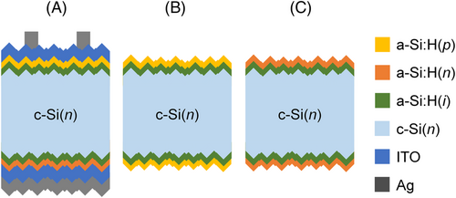
For the fabrication of the SHJ solar cells, a stack of intrinsic and p-type a-Si:H [a-Si:H(i) and a-Si:H(p), respectively] layers was formed on the front side using a PECVD system. A stack of a-Si:H(i) and n-type a-Si:H [a-Si:H(n)] films was deposited on the rear side using the same system. The thicknesses of the a-Si:H(i) and doped a-Si:H films are between 6–7 and 10–15 nm, respectively. A 75-nm indium tin oxide (ITO) film was then deposited on the front side by a sputtering system through a mask to form active areas of 2 × 2 cm2. The front grid metallisation was achieved by screen-printing of low temperature silver (Ag) paste followed by a curing process at 200°C for 30 min in air ambient. The rear contact was formed by a full-area stack of 240-nm sputtered ITO and 240-nm sputtered Ag layers. Further details regarding the PECVD and sputtering deposition conditions can be found in Balaji et al.27
To investigate the temperature-dependent behaviour of the a-Si:H-based passivating contacts, symmetrical lifetime structures for τeff measurements and J0s extraction were prepared. These structures were passivated with either a-Si:H(i/p) or a-Si:H(i/n) stack on both sides.
All the test structures were annealed at 200°C for 30 min in air ambient to mimic the thermal budget of the Ag paste curing process. Sketches of all the studied cells and test structures are shown in Figure 1.
2.2 Characterisation
Current–voltage (I-V) measurements of SHJ solar cells were performed by an I-V tester from 25°C to 70°C, while Suns-Voc measurements were done using a customised Suns-Voc system28, 29 from 80°C to 30°C. The uncertainty associated with the temperature controller for both measurement tools is estimated at ±0.1°C. After reaching the set temperature, the solar cells were left on the heated stage for 10 min to stabilise before the measurements were done. At the completion of the temperature scan, the measurement was repeated at 25°C to ensure that the properties of the solar cells were not modified by this scan.
TCs are determined from the slopes of the linear fits of the cell parameters as a function of temperature.30 They are normalised to the cell parameters at 25°C and presented as relative TCs in this study.
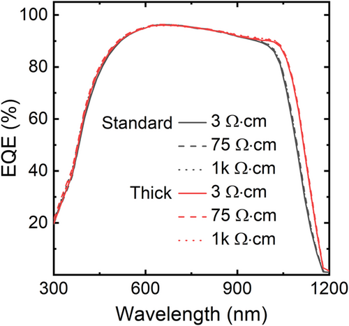
A spectral response system (QEX7, PV Measurements Inc.) was used to measure the external quantum efficiency (EQE) of the studied solar cells.
The symmetrical lifetime test structures were used for τeff measurements in the temperature range from 25°C to 80°C using a WCT-120TS lifetime tester (from Sinton Instruments).31 The Kane–Swanson method32 is used to extract J0s from the τeff curves. The model of Richter et al.33 is used to calculate the intrinsic lifetime, while the bandgap narrowing model of Schenk34 and the model of Klaassen35 are used to determine the effective intrinsic carrier concentration (ni,eff) and the mobility, respectively.
Based on previous studies,36-38 light and elevated-temperature induced degradation (LeTID) should be considered when heating and illuminating Si wafers. However, it was reported that in n-type FZ wafers, after 5 s of light soaking at 140°C and light intensity of one-sun, τeff reduces by less than 5%.36 In this study, all the measurements were shorter than 5 s and at lower temperatures (25°C–80°C); hence, a significant impact by LeTID is not expected. Furthermore, the measurements at 25°C before and after the temperature scan are identical, confirming that LeTID does not affect the studied cells.
3 RESULTS AND DISCUSSION
3.1 Temperature-dependent performance of SHJ solar cells at one-sun
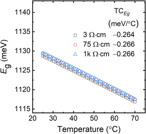
The cell parameters of the SHJ solar cells with different wafer resistivities fabricated using standard thickness and thick wafers at one-sun as a function of temperature are shown in Figure 2A–H. Overall, as expected, the Voc, FF, pseudo fill factor (pFF, fill factor without the effects of series resistance), and the efficiency decrease, whereas the short-circuit current density (Jsc) increases at elevated temperatures.30 The reduction of Voc, FF, and pFF can be explained by the increase of ni,eff with increasing temperature caused by bandgap narrowing.39 This effect also explains the improvement of Jsc.30 Non-linear behaviour of FF in the temperature range between 25°C and 40°C, regardless of the wafer resistivity and thickness, is observed. This phenomenon commonly occurs in SHJ solar cells and is usually attributed to thermionic barriers at the heterojunctions in these cells.40
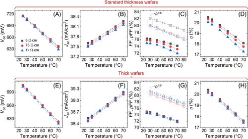
Interestingly, for the standard thickness cells, the decrease of Voc at elevated temperatures is less pronounced with decreasing wafer resistivity while the decrease of Voc at elevated temperatures is almost identical regardless of the wafer resistivity in the case of the thicker cells. We will discuss further on these observations in the latter part of this section.
The efficiency of the cells as a function of temperature is presented in Figure 2D,H. At STC, the efficiency of the standard thickness cells slightly decreases with increasing wafer resistivity, mainly due to FF, whereas the thick cells' efficiency is almost identical. The superior Voc and FF of the standard thickness cells overcompensate for their lower Jsc, and therefore their efficiency is slightly higher than the thick cells. At elevated temperatures, as expected, the reduction in efficiency is more pronounced with increasing wafer resistivity for the standard thickness cells because of the temperature dependence of both the Voc and FF. Meanwhile, this reduction is almost identical for the thick cells regardless of the wafer resistivity. Note that the non-linear behaviour of the efficiency in the temperature range between 25°C and 40°C regardless of the wafer resistivity and thickness is due to FF, as depicted in Figure 2C,G.
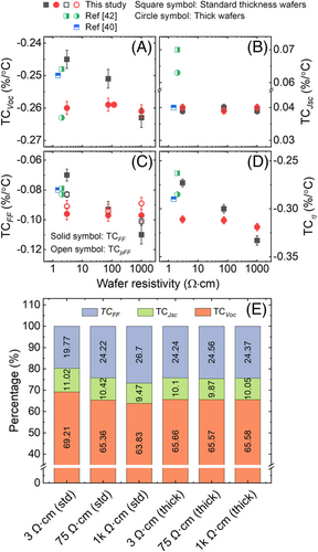
Figure 3A clearly shows that the Voc of the standard thickness cells is more sensitive to temperatures with increasing wafer resistivity, while the thick cells' TCVoc is almost independent of the resistivity. TCVoc of the latter cells is nearly equal to that of the standard thickness cell with wafer resistivity of 1k Ω⋅cm. The obtained TCVoc are comparable to those previously reported.42 The superior TCVoc of thinner cells has been also reported in the same reference.
| Wafer resistivity (Ω⋅cm) | Gamma factor (γ) | |
|---|---|---|
| Standard thickness wafers | Thick wafers | |
| 3 | 1.3 | 1.8 |
| 75 | 1.8 | 1.7 |
| 1k | 2.6 | 1.7 |
- Abbreviations: SHJ, Si heterojunction; STC, standard testing conditions.
From Figure 3B, it seems that the TC of Jsc (TCJsc) is almost identical regardless of the wafer resistivity and thickness, highlighting the interesting point that was discussed above. The obtained TCJsc are comparable to that reported in Haschke et al.40 and lower than those presented in Sai et al.42 This difference might be due to the spectrum-dependent TCJsc when using different solar simulators.48 The contribution of TCJsc to TCη is the smallest for all the studied cells (see Figure 3E).
In Figure 3C, it can be seen that TCFF of the 3-Ω⋅cm standard thickness cell is better than its TC of the pFF (TCpFF), while the opposite trend is observed for the 1k-Ω⋅cm standard thickness cell. Meanwhile, the TCFF of the standard thickness cell with the wafer resistivity of 75 Ω⋅cm and all the thick cells is almost identical to their TCpFF. This highlights a different temperature dependence of Rs. Compared to the literature,40, 42 the obtained TCFF of the 3-Ω⋅cm standard thickness cells is slightly better while that of the 3-Ω⋅cm thick cells is slightly worse. Note that Sai et al.42 also reported better TCFF for thinner cells.
As expected, the TCη of all the investigated cells is dominated by TCVoc, with a contribution above 60%, regardless of the wafer resistivity and thickness (see Figure 3E). It is therefore not surprising that the TCη of the standard thickness cells becomes worse with increasing wafer resistivity, while it is almost identical for the thick cells. The obtained TCη are slightly lower compared to the values reported in Sai et al.42 (3-Ω⋅cm cells), mainly due to the higher TCJsc of the cells in this reference.
From the above discussion, we find that the temperature dependence of Voc dominates that of the cell performance regardless of the wafer resistivity and thickness. Therefore, it is important to gain a deeper understanding regarding the impacts of passivating contacts on the cells' TCVoc as well as knowledge regarding their performance at different illumination intensities (as usually occur in the field). In the next sections, we will focus on these two aspects.
3.2 Temperature dependence of surface passivation
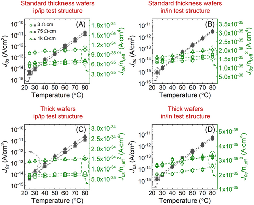
To assess the temperature dependence of the surface passivation, J0s values were extracted from τeff measurements of symmetrical test structures and are presented in Figure 4A–D. The τeff at Δn = 1015 cm−3 and 25°C are summarised in Table C1 (Appendix C). At 25°C, the extracted J0s values are comparable to those reported in Le et al.49 At elevated temperatures, as expected, J0s significantly increases regardless of the wafer thickness or the configuration of the test structures. It is due to an increase of ni,eff by several orders of magnitude.32 The J0s/ni,eff2 ratio as a function of temperature is also presented in the figures. This ratio increases with increasing temperature indicating a slight reduction of the passivation quality at elevated temperatures. Bernardini et al.50 also reported an increase of the surface recombination velocity of FZ n-type Si wafers passivated by 50-nm a-Si:H(i) layers with increasing temperature, which is consistent with our findings. values extracted from the linear fits of J0s/ni,eff2 ratio as a function of temperature are provided in Table 2.
| Wafer resistivity (Ω⋅cm) | (%/°C) | |||
|---|---|---|---|---|
| Standard thickness wafers i/p | Standard thickness wafers i/n | Thick wafers i/p | Thick wafers i/n | |
| 3 | 0.43 ± 0.03 | 0.48 ± 0.05 | 0.35 ± 0.05 | 0.43 ± 0.08 |
| 75 | 0.21 ± 0.04 | 0.41 ± 0.07 | 0.21 ± 0.01 | 0.46 ± 0.06 |
| 1k | 0.24 ± 0.03 | 0.53 ± 0.04 | 0.18 ± 0.03 | 0.51 ± 0.08 |
- Abbreviation: TC, temperature coefficients.
For standard thickness wafers, the reduction of the passivation quality of the a-Si:H(i/p)-based test structures is less pronounced for wafers with high resistivity (75 Ω⋅cm and above). Meanwhile, the reduction of the passivation quality of the a-Si:H(i/n)-based test structures is almost identical regardless of the wafer resistivity. Similar trends are observed for the test structures using thick wafers. Interestingly, values of the a-Si:H(i/p)-based and a-Si:H(i/n)-based test structures are almost the same for the standard thickness and thick wafers. Nevertheless, it seems the observed reduction in the passivation quality in all the cases has only an insignificant impact on TCVoc. The temperature-dependent behaviour of Voc and hence TCVoc, is still dominated by that of ni,eff.
3.3 Injection and temperature dependence of SHJ solar cells
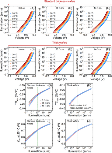
In the previous sections, we discussed the temperature-dependent performance of the investigated cells and test structures at one-sun. However, in the field, solar cells operate not only at different temperatures, but also under a wide range of illumination intensities. Therefore, insights into their performance at combinations of various temperatures and intensities are of significant interest. In this section, we use temperature-dependent Suns-Voc measurements in between 0.001 and >100 suns to extract TCVoc as a function of illumination intensity. This information can be used to predict the temperature sensitivity of the cells at different illumination intensities as TCVoc dominates TCη for all the investigated cells.
Figure 5A–F presents the Suns-Voc measurements in the temperature range from 30°C to 80°C. A significant reduction of Voc with increasing temperature at low illumination intensities can be observed regardless of the wafer resistivity and thickness. This reduction becomes less pronounced at higher illumination intensities (above one-sun). The extracted relative TCVoc values from the Suns-Voc measurements as a function of illumination intensity are presented in Figure 5G,H as open symbols. For comparison, TCVoc values obtained from I-V measurements (solid symbols) at one-sun are also shown. As can be seen, TCVoc values at one-sun extracted from both methods match very well (in the range of 2% and 0.2% for the standard and thick cells, respectively), supporting the observed trend of the temperature-dependent Voc as discussed in Section 3.1. All the investigated cells are more sensitive to temperature variation at lower illumination intensities as indicated by the more negative TCVoc. Interestingly, below one-sun, the illumination intensity dependence of TCVoc is more pronounced for the standard thickness cells using higher resistivity wafers. Meanwhile, the TCVoc values of the thick cells behave the same across the entire measured intensity range regardless of the wafer resistivities. To clarify this observation, the extracted Voc values at 25°C are presented in Figure 5I,J. In most of the illumination range, the trend of TCVoc can be explained by that of the initial Voc. However, for the standard thickness cells, it seems that γ has a significant impact on their TCVoc in the illumination range of 0.3–2 suns in which their TCVoc become more negative with increasing wafer resistivity despite their similarly initial Voc.
4 CONCLUSION
The temperature- and illumination-dependent performance of SHJ solar cells using high wafer resistivities (up to 1000 Ω⋅cm) was investigated. The TCs of the main electrical cell parameters of these cells are almost independent of the wafer resistivity. Furthermore, we also found that the investigated cells are more sensitive to temperature variation at lower illumination intensities. The findings of this study demonstrate that there is no limitation in using very high-resistivity wafers for SHJ solar cells under field operating conditions. The study, therefore, set a premise for using such wafers for reducing the Auger recombination and to push SHJ solar cell efficiency towards their theoretical efficiency limit.
ACKNOWLEDGEMENTS
This work was funded by the Australian Government through Australian Renewable Energy Agency [ARENA; project 2017/RND001]. The views expressed herein are not necessarily the views of the Australian Government, and the Australian Government does not accept responsibility for any information or advice contained herein. This material is also based upon work supported by the U.S. Department of Energy's Office of Energy Efficiency and Renewable Energy (EERE) under the Solar Energy Technology Office (SETO), award number DE-EE0008549 and by the U.S. Department of Energy, PV Foundry, grant DE-EE0008975. Open access publishing facilitated by University of New South Wales, as part of the Wiley - University of New South Wales agreement via the Council of Australian University Librarians.
APPENDIX A: EQE SPECTRA OF THE INVESTIGATED CELLS
APPENDIX B: BANDGAP NARROWING OF SI AT ELEVATED TEMPERATURES
APPENDIX C: τeff OF THE SYMMETRICAL LIFETIME TEST STRUCTURES AT Δn = 1015 cm−3 AND 25°C
| Wafer resistivity (Ω⋅cm) | τeff at Δn = 1015 cm−3 and 25°C (ms) | |||
|---|---|---|---|---|
| Standard thickness wafers i/p | Standard thickness wafers i/n | Thick wafers i/p | Thick wafers i/n | |
| 3 | 1.41 | 2.72 | 2.21 | 4.72 |
| 75 | 2.40 | 2.75 | 2.14 | 8.64 |
| 1k | 1.48 | 1.28 | 2.45 | 5.52 |
Open Research
DATA AVAILABILITY STATEMENT
The data that support the findings of this study are available on request from the corresponding author. The data are not publicly available due to privacy or ethical restrictions.


