Research progress and applications of optoelectronic synaptic devices based on 2D materials
Yukun Zhao, Linrui Cheng and Rui Xu are contributed equally to this work.
Abstract
In the natural world, the human brain is the most powerful information processor, using a highly parallel, efficient, fault-tolerant, and reconfigurable neural network. Taking inspiration from this impressive architecture, optoelectronic synaptic devices have gained considerable attention for their ability to process and retain data simultaneously, making them essential components in the upcoming era of neuromorphic computing systems. In recent years, significant progress has been made in the development of optoelectronic neuromorphic synaptic devices using two-dimensional (2D) material heterostructures. This review focuses on the use of 2D materials in creating optoelectronic synaptic devices. It discusses the recent progress made in utilizing 2D material heterostructures in these devices and examines their potential in different areas such as image recognition, neuromorphic wearable electronics, logical operations, and neuromorphic computing systems. Heterostructures made with 2D materials provide a wide range of possibilities as their electronic band structures can be easily tailored to achieve effective optical and electrical modulation. Optoelectronic synaptic devices based on 2D materials simultaneously exhibit two functionalities: detection and memory. Furthermore, these materials have strong interatomic bonding within layers and possess a thickness of only one atomic layer, giving them exceptional flexibility, optical transparency, and mechanical strength. By utilizing 2D materials for solution processing and their ultra-thin profile, the manufacturing of three-terminal synapses becomes cost-effective, simplifying integration processes.
Key points
What is already known about this topic?
-
Two-dimensional (2D) materials, particularly those that include heterojunctions, have the potential to imitate the plasticity observed in biological synapses. As a result, these materials offer promising opportunities for the advancement of artificial optoelectronic synaptic devices.
What does this study add?
-
This review offers a thorough analysis of 2D materials, focusing specifically on optoelectronic synaptic devices made from 2D heterostructures. It also explores the potential applications of these devices in various fields, including image recognition, neuromorphic wearable electronics, logical operations, and neuromorphic computing systems.
1 INTRODUCTION
In traditional computer systems, the physical separation of data processing and storage in the von Neumann architecture leads to significant energy consumption and decreased computing speed.1, 2 As the demand for processing big data in the Internet era continues to grow, this limitation becomes more apparent.3, 4 The neural network of the human brain, a naturally occurring information processor, demonstrates exceptional efficiency and fault tolerance. Importantly, it possesses parallel processing capabilities, reconfigurability, low energy consumption, and the ability to perform complex functions such as image recognition and self-learning.3, 5-7 As a result, there is a growing interest in the implementation of hardware computing, specifically neuromorphic computing, which aims to mimic the architecture of the human brain.8 The neural network present in the human brain consists of multilayered neurons and synaptic connections among these neurons.9, 10 Neurons function as units for processing information, while synapses enable the transmission of signals and exchange of information.7 The strength of connectivity between neurons is known as synaptic weight.7 Consequently, the development of biomimetic artificial synaptic devices that possess biological synaptic functions is of paramount importance in realizing neural morphology computation.11
Drawing inspiration from the human brain, the regulation of synaptic weights by visual neurons can achieve crucial functions such as learning and visual information memory.7 Optoelectronic synaptic devices take advantage of high-bandwidth, low-crosstalk, low-power, and instantaneous optical signals as input.2, 5 By modulating device conductivity to regulate synaptic weights, these devices can accomplish visual signal perception, information processing, and data memory in a way that closely resembles biological synapses.2, 5, 12-14 Moreover, the noncontact input feature of optoelectronic synaptic devices minimizes the influence of Joule heat, leading to faster processing speeds.15 Furthermore, by adjusting various parameters such as wavelength, frequency, and power density of the optical input signal, the efficiency of conductivity regulation can be enhanced.15, 16 Therefore, the advancement of optoelectronic synaptic devices holds significant importance for the successful realization of neuromorphic brain computing.17
In the biological system, synaptic plasticity refers to the ability of synapses to exhibit a range of synaptic weights in response to different stimuli, effectively performing “calculation” tasks. Changes in synaptic weights occur as responses to specific stimuli, representing the “storage” function.18, 19 In simple terms, synaptic plasticity, closely associated with memory, learning, recognition, and other brain functions, is manifested through alterations in synaptic weight.18 The effectiveness of synapses is typically evaluated by modulating the postsynaptic current (PSC), which includes both excitatory postsynaptic current (EPSC) and inhibitory postsynaptic current (IPSC). Different characteristics of synaptic plasticity, such as short-term plasticity (STP) and long-term plasticity (LTP), can be observed through various techniques for regulating PSC.20 Therefore, simulating synaptic plasticity is an important endeavor in achieving neural morphology calculations.
Optoelectronic synaptic devices exhibit the capability to perform light perception, signal processing, and memory simultaneously.6 These devices use light signals to imitate the action potential observed in presynaptic biological neurons and employ two sets of electrodes (up/down or source/drain) to replicate the presynaptic/postsynaptic membranes. The changes in specific parameters, such as resistance and conductivity, within synaptic devices reflect the modifications observed in biological synaptic weights.6 Upon exposure to light stimulation, the conductivity of the active materials within synaptic devices is modified. This modification leads to changes in resistance or potential, resulting in the generation of either EPSC or IPSC. The intensity of the current is determined by the synaptic weight and can be stored in different resistance states. Importantly, even after the light stimulation stops, the synaptic device does not immediately return to its original state, thus exhibiting distinct synaptic characteristics.16 In recent years, the field of optoelectronic synaptic devices has witnessed the emergence of two-dimensional (2D) materials as highly promising candidates. These materials possess exceptional properties that make them particularly suitable for this application. For example, when a 2D WOx/WS2 heterostructure is positioned between two silver electrodes, it displays modulated electrical resistance and operates effectively at low voltage levels. Additionally, memristors constructed using this structure exhibit low ON-state resistance and high switching ratios.21 The broadband optical response of these materials enables the creation of artificial synapses and nonvolatile memory, facilitating rapid reconfiguration within a single device to serve its intended purpose.22 Moreover, 2D materials have the potential to achieve channel gate-tunable memristive switching functions, offering new possibilities for achieving plasticity in multi-terminal heterosynapses.21
This review primarily focuses on optoelectronic synaptic devices constructed using 2D Van der Waals (vdW) heterostructures. Figure 1 provides an overview of the 2D materials used in fabricating optoelectronic synaptic devices, along with their fundamental structure and potential applications. Initially, the categorization of 2D materials in optoelectronic synaptic devices is thoroughly explained. Subsequently, the review explores the introduction of optoelectronic synaptic devices from four distinct perspectives: heterostructures, working mechanisms, device structures, and preparation methods. Heterostructures are discussed in terms of both two-terminal and three-terminal configurations. Importantly, the review also investigates the potential and applications of optoelectronic synapses in areas such as image recognition, neuromorphic wearable electronic devices, logical operations, and neuromorphic computing systems, providing valuable insights for future development endeavors.
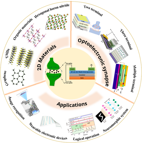
2D Materials, structures, and applications of artificial optoelectronic synaptic devices.23-30 Copyright © 2012, Springer Nature Limited. Copyright © 2018 American Chemical Society. This publication is licensed under these Terms of Use. © 2018 WILEY-VCH Verlag GmbH & Co. KGaA, Weinheim. Copyright © 2020, American Chemical Society. Copyright © 2018, Seunghwan Seo et al. Copyright © 2021, American Chemical Society.
2 TWO-DIMENSIONAL MATERIALS
An important consideration in developing optoelectronic synaptic devices is the selection of functional materials. These materials can be broadly categorized into four groups: metal oxides, silicon materials, organic materials, and low-dimensional materials. Metal oxides offer several advantages, such as high carrier mobility and excellent transparency.20 On the other hand, silicon materials are compatible with complementary metal-oxide-semiconductor (CMOS) processes and offer significant benefits in terms of production and application.31 Organic materials are preferred for their low cost and biocompatibility.32 In recent years, low-dimensional nanomaterials have gained considerable attention in optoelectronic conversion due to their nonlinear optical properties, high photosensitivity efficiency, easy preparation methods, good conductivity, low leakage current, and wide bandgap.20, 33-35 The remarkable attributes of 2D materials and their stacked heterostructures, including their nearly atomic thinness, extremely high light sensitivity, substantial opto-current switch ratio, exceptional optical gain, rapid response time, and extremely low dark current, have sparked significant interest in the field of optoelectronic synaptic devices (Figure 2A).17, 36 With a wide range of unique benefits, 2D materials encompass various categories including insulators, semiconductors, semimetals, and metals.37 The adjustability of their carrier concentration and mobility allows for the realization of synaptic plasticity and neuromorphic computing through carrier dynamics.37-39 The weak charge shielding ability of these materials makes electrons susceptible to factors such as electric and magnetic fields, as well as interface defects during transportation within the material.18 This characteristic enables the achievement of different conductivity states with low power consumption, thereby facilitating the simulation of synaptic plasticity.40 Therefore, the following paragraphs will primarily focus on the application of 2D materials in the development of synaptic devices.
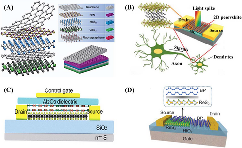
(A) Van der Waals heterojunction. In Ref.66 Copyright © 2013, Springer Nature Limited. (B) Light stimulation of artificial synapses prepared by 2D perovskites.60 © 2019 WILEY-VCH Verlag GmbH & Co. KGaA, Weinheim. (C) Schematic diagram of the organic–inorganic hybrid heterojunction. In Ref.63 © 2018 WILEY-VCH Verlag GmbH & Co. KGaA, Weinheim. (D) Schematic diagrams of the BP/ReS2 heterostructure device and the lattice arrangement at the junction interface. In Ref.65 © 2020 WILEY-VCH Verlag GmbH & Co. KGaA, Weinheim.
The mobility of electrons in 2D materials is significantly enhanced compared to their three-dimensional (3D) counterparts due to the presence of single or multiple atomic layers. This increase in electronic conductivity has been demonstrated in various studies.41, 42 In a 2D plane, the atoms within the inner layer are bonded by covalent bonds, while the interlayers are held together by weak vdW forces. Consequently, 2D materials with multiple atomic layers can be exfoliated into single layers, thereby improving their functionality.43-46 Moreover, 2D materials exhibit a highly adjustable light response across a broad range of wavelengths, from ultraviolet (UV) to near-infrared.16, 41 The ultrathin nature of these materials also facilitates fast heat dissipation.47 Additionally, the composition, crystal structure, and layer thickness of 2D materials can be modified to alter their properties.44, 48 Therefore, there is significant anticipation regarding the progress of optoelectronic synaptic devices that utilize 2D materials. These materials offer potential advantages such as small size, low energy consumption, high performance, and exceptional reliability.49, 50 Currently, the variety of 2D materials used in the production of optoelectronic synaptic devices includes graphene, transition metal chalcogenides (TMDs), and 2D organic materials, among others.
2.1 Graphene
Graphene, the first 2D material studied, possesses attributes such as high carrier mobility, elevated thermal conductivity, remarkable optical transparency, and robust thermal stability.41 Due to its zero bandgap, intrinsic graphene exhibits semi-metallic properties. Furthermore, graphene is known for its higher contact resistance and weaker vdW forces, both of which contribute to reduced operating currents when used as an electrode.51 For example, Yu et al. utilized a heterostructure consisting of graphene and MoS2 to fabricate an optoelectronic transistor.52
2.2 Transition metal chalcogenides
TMDs, such as MoS2, WS2, WSe2, have attracted significant attention due to their large and adjustable bandgaps.41, 43 TMDs typically have an X-M-X structure, with three layers of atoms that exhibit notable anisotropy. In this structure, X represents a sulfur group element, while M denotes a transition metal element.43 The optoelectronic adjustability, flexibility, and atomically smooth surfaces of TMDs make them suitable for high integration density and scalability, enabling rapid switching and reduced power consumption.53, 54 Most semiconductor TMDs have a bandgap that increases as the number of layers decreases. Importantly, the electronic band structure of TMDs has the potential to transition from an indirect to a direct bandgap, thereby enhancing the switch ratio of the fabricated devices.43 Furthermore, their exceptional optical transparency and flexibility make them suitable for the fabrication of flexible transparent devices.
MoS2 is a typical 2D material of the TMDs. It is abundantly available in nature and known for its exceptional properties, such as strong thermal stability and flexibility between layers.55 Interestingly, when MoS2 is reduced to a single layer, its bandgap transitions from an indirect to a direct configuration.55 By exploiting this phase transition and its high switch ratio, researchers have successfully developed artificial synapses using MoS2.53 Li et al. observed switched characteristics in memristors as a result of the modulation of the MoS2/metal Schottky barrier and the redistribution of vacancies within the MoS2 channels.56 Additionally, Liu et al. created optoelectronic synaptic devices by integrating 2D phosphorene with MoS2.57 Furthermore, Roy et al. found that the heterojunction formed by combining MoS2 with graphene exhibits high sensitivity for photodetection and persistent photoconductivity.58
2.3 Two-dimensional organic materials
2D organic materials offer great flexibility and can be easily processed in a solution. By adjusting their chemical structure and thickness, their response to external signals can be controlled, making them suitable for the large-scale production of low-cost and flexible synaptic devices. For instance, Fang et al. used solution epitaxy to create a photo-stimulated synaptic transistor using 2D organic semiconductor materials.47 Additionally, the organic–inorganic hybrid perovskite has attracted significant research attention in the optoelectronic device field due to its advantageous properties, such as a prolonged carrier lifespan, diffusion length, and high light absorption coefficient.24, 59 Sun et al. used 2D layered perovskite to create synaptic photoconductors that can imitate synaptic behavior when exposed to light (Figure 2B).60 They discovered that the photoelectric properties of 2D layered perovskites can be precisely adjusted through chemical composition engineering, presenting a new platform that fulfills the complexity necessary for neural morphology calculations.60 Similarly, Liu et al. employed 2D metal–organic framework thin films as active layers to develop optoelectronic synaptic devices. These devices demonstrated fundamental synaptic activities such as LTP and STP, along with remarkable synaptic plasticity.61 In addition, Lai et al. combined 2D Ruddlesden–Popper phase layered perovskites with organic semiconductors to form type II heterojunctions. Their experiment revealed that these heterojunction systems can simulate fundamental properties of biological synapses, including EPSC, paired-pulse facilitation (PPF), and the transition from short-term memory (STM) to long-term memory (LTM) states.62 Moreover, Wang et al. integrated 2D inorganic and organic materials to fabricate an organic/inorganic hybrid heterostructure synaptic transistor, which not only demonstrated robust optical and electrical modulation but also exhibited STP and LTP characteristics (Figure 2C).63
2.4 Other two-dimensional materials
In addition to the aforementioned 2D materials, there are other materials used in the production of optoelectronic synaptic devices. For example, Oh et al. utilized the optical memory phenomenon in hexagonal boron nitride (h-BN) to create a photoelectroactive synapse. This achievement was made possible by creating a heterojunction between h-BN and MoS2. It is important to note that optical stimuli can either enhance or suppress changes in synaptic weights.64 Organic–inorganic halide perovskites (OIHPs) demonstrate impressive optical properties and are widely considered promising candidates for artificial synapses.24 The optical and electrical characteristics of 2D layered OIHPs can be readily manipulated by modifying their composition.24 However, despite their exceptional optical properties, OIHPs only exhibit temporary changes in conductivity when exposed to light. Additionally, the conductivity rapidly decreases after the light is turned off due to the recombination of photoexcited charge carriers.24 Park et al. developed an optical synapse by effectively combining a 2D layered OIHP with the transparent oxide semiconductor indium zinc tin oxide (IZTO). This optical synapse capitalizes on the high light absorption capacity of OIHP, enabling efficient stimulation by light spikes. The favorable band alignment between IZTO and OIHP also facilitates the efficient spatial separation of photoexcited charge carriers, resulting in nonvolatile changes in conductivity.24 Furthermore, Xiong et al. successfully demonstrated the application of a 2D vdW heterostructure by combining black phosphorus (BP) with rhenium disulfide (ReS2) in logic circuits (Figure 2D).65
3 OPTOELECTRONIC SYNAPTIC DEVICES BASED ON TWO-DIMENSIONAL HETEROSTRUCTURES
2D materials have attracted significant attention and research in the field of optoelectronics due to their exceptional physical properties and atomic-level thickness. These materials can exhibit plasticity similar to that observed in biological nerve synapses under certain conditions. Optoelectronic synaptic devices offer compatibility with both light and electrical stimulation.16 The synaptic weight can be adjusted by applying optical signals to the device, allowing control of parameters such as duration, frequency, and power of the light pulse.31 2D materials possess several advantages, including low crosstalk, wide spectral response, and robust stability, which make them promising for high-density integration and low power consumption in optoelectronic synapses.18, 41, 55
3.1 Two-dimensional heterostructures
In addition to individual 2D materials, heterostructures formed from these materials have been extensively researched due to their enhanced optoelectronic properties and diverse characteristics.48, 66, 67 The weak vdW interlayer forces enable the extraction of various 2D materials, allowing their reassembly into arbitrarily stacked heterostructures.68 Heterostructures based on 2D materials exhibit excellent scalability and efficient photon–electron conversion efficiency, enhancing density.3, 20, 69 Compared to single materials, the energy band arrangement and carrier mobility of stacked 2D materials within heterostructures can be further adjusted, significantly improving the photoelectric properties.42, 53, 67, 70, 71 Through the precise design of the material arrangement and composition, it becomes possible to realize multifunctional applications of 2D materials. Moreover, this approach is expected to greatly enhance the functional integration density and reliability of optoelectronic synaptic devices for multifunctional applications.72, 73
There are two types of heterostructures: vertical and lateral.42, 74 Vertical heterostructures involve the stacking of different 2D materials layer by layer in the vertical direction,42 with vdW forces between layers that are not limited by lattice matching.75 For example, Zheng et al. produced high-quality and large-area WS2(1–x) Se2x/SnS2 vertical heterostructures using a two-step chemical vapor deposition (CVD) method.76 On the other hand, lateral heterostructures are formed by connecting different 2D materials on the same plane, typically through covalent bonds, resulting in sharp atomic-level transitions at the junction.42 For example, Duan et al. created compositionally controlled lateral heterostructures of MoS2–MoSe2 and WS2–WSe2 by manipulating the reactants in the vapor phase while growing 2D crystals. Their experimental results showed that the WS2–WSe2 heterojunction formed a lateral p–n diode with outstanding performance in terms of current rectification and photocurrent generation.77 Additionally, Zhang et al. achieved the synthesis of lateral heterostructures of MoS2–WS2 and MoSe2–WSe2 using ambient-pressure CVD.78
Heterojunctions are commonly classified into three types, namely type I, type II, and Type III, based on their electronic band structure, as depicted in Figure 3.79, 80 In type I heterostructures (Figure 3A), the minimum of the conduction and valence bands are both located within the same material.75 Conversely, in type II heterostructures (Figure 3B), the minimum of the conduction band and the maximum of the valence band are situated in two distinct materials. Type II heterojunctions have garnered significant attention due to their remarkable light response characteristics and substantial rectification ratio. They effectively separate electrons and holes, thereby prolonging the exciton lifetime and regulating the photovoltaic and rectification properties.67, 74 For example, at the interface of MoS2/GaSe, an inherent electric field arises due to the difference in energy between the valence and conduction bands. This leads to the formation of a space charge region. Additionally, potential barrier peaks are created to restrict the movement of electrons.81 When a forward voltage is applied to the source and drain electrodes, the strength of the inherent electric field decreases, leading to a decrease in the height of the potential barrier. This reduction facilitates the movement of electrons across the barrier, resulting in an increase in forward current. On the other hand, when a reverse voltage is applied, the strength of the built-in electric field intensifies. As a result, the energy of the electrons is no longer sufficient to overcome the potential barrier, leading to minimal current between the source and drain electrodes.55 Type III heterostructures exhibit pronounced staggered gaps (Figure 3C) with no overlap between band gaps, leading to the formation of a discontinuous band gap. This specific heterostructure is extensively utilized in tunnel field-effect transistors.80, 82, 83

(A) Type I, (B) Type II, and (C) Type III heterojunctions. In Ref.80 © 2017 WILEY-VCH Verlag GmbH & Co. KGaA, Weinheim.
The vast range of 2D materials is essential for the advancement of heterojunctions with various properties. For instance, in 2019, Wang et al. introduced a hybrid heterojunction synaptic transistor that combines MoS2 and perylene-3,4,9,10-tetracarboxylic dianhydride (PTCDA).63 The adjustable gate band configuration of the type II heterojunction enables the introduction of charge carriers into MoS2. By employing mechanisms like separation, capture, and controlled release of carriers at the interface of the heterojunction, the vital functions of biological synapses are replicated.63 In 2021, Luo conducted a study on synthesizing a heterojunction using gold nanoparticles (Au NPs) and MoS2.84 The addition of Au NPs to the heterojunction resulted in enhanced light absorption through plasmon effects. Consequently, the photoluminescence intensity increased, and a maximum carrier mobility of 20.04 cm2·V−1 s−1.84 To address the problems of nonlinearity and conductivity saturation caused by the built-in electric field at the interface of 2D materials/electrodes, Hao et al. introduced a vertical heterostructure using thin films of MoS2 and WO3. The function of WO3 is to serve as a stable anion reservoir, efficiently absorbing and releasing anions to enhance the linearity of conductivity changes.85 In 2022, recognizing that laterally designed memory transistors pose challenges for integration, Wang et al. devised a vertical vdW heterostructure composed of graphene/CuInP2S6 (CIPS)/MoS2/h-BN.86 Serving as asymmetric electrodes, graphene and MoS2 correspond to pre- and post-neurons, respectively. Experimental findings indicate that the bias voltage of the resistance switch closely aligns with the coercive voltage of the CIPS flake. This alignment suggests that the reversal of ferroelectric polarization drives the behavior of a resistance switch.86 Recently, Syed et al. demonstrated the modulation of excitation and inhibition using a type II 2D heterostructure opto-memristive neuron. This allows for the nonlinear integration of excitatory and inhibitory postsynaptic potentials within a single device.87
3.2 Working mechanisms
Optoelectronic synaptic devices that utilize 2D materials primarily function by capturing and releasing charges either within the materials themselves or at their interfaces. This enables their functional capabilities.3 These charge transfer mechanisms are influenced by various factors, including the density of charge capture points at the interface of the 2D material/substrate.3, 26, 48, 60 Figure 4A depicts the classification of optoelectronic synaptic devices powered by 2D materials. These devices can be grouped into several categories, such as intrinsic 2D material channels with or without functional oxide interfaces, 2D materials integrated with nanoparticles or quantum dots, 2D vdW heterostructures, and 2D ferroelectric materials.3 Among them, optoelectronic synapses based on 2D heterojunctions mimic synaptic behavior through the charge capture/release process that occurs at the interfaces of specific 2D layers within heterostructures.3, 88
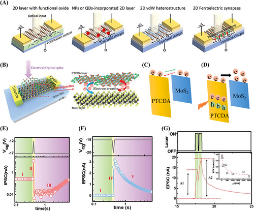
(A) Working mechanism diagrams of optoelectronic synaptic devices that rely on 2D materials and their different forms. In Ref.3 Copyright © 2022, Yoo, Changhyeon; Ko, Tae-Jun et al. This article is distributed under a Creative Commons Attribution (CC BY) license. (B) MoS2/PTCDA hybrid heterojunction exhibits synaptic behavior due to electron transfer at its interface. In Ref.63 © 2018 WILEY-VCH Verlag GmbH & Co. KGaA, Weinheim. (C) Charge transfer under electrical pulse stimulation. (D) Charge transfer under laser pulse stimulation. (E) IPSC and (F) EPSC under electrical pulse stimulation. (G) EPSC under laser pulse stimulation. In Ref.63 © 2018 WILEY-VCH Verlag GmbH & Co. KGaA, Weinheim.
Using the heterojunction consisting of 2D MoS2 and PTCDA as an example (Figure 4B), the combination of these materials creates a type II heterojunction. The band alignment of this particular heterojunction can be adjusted by the gate, allowing for the injection of carriers into MoS2 through both electrical and optical means. Within the interface of the heterojunction, carriers can undergo separation, capture, and gradual release, giving rise to synaptic behavior such as STP and LTP.63 When a specific gate voltage is applied, carriers within the MoS2/PTCDA synaptic transistor heterojunction reach dynamic equilibrium, maintaining a stable drain–source current (Ids).63 Upon application of a positive gate voltage pulse, more electrons accumulate in the channel of MoS2, resulting in an increase in Ids. At the same time, the electric field at the gate weakens and the band bends, causing some electrons to transfer to PTCDA. Consequently, the number of electrons in MoS2 decreases, leading to a decrease in Ids. Since the migration rate is low, electrons in PTCDA slowly diffuse back to MoS2, gradually restoring Ids to the reference level within a few seconds, resulting in IPSC (Figure 4C–E). Conversely, when negative electrical pulses are applied, the direction of charge transfer reverses, resulting in EPSC, as illustrated in Figure 4F. Upon being stimulated by a laser pulse, a significant number of unbalanced electrons, created by the laser pulse, migrate from PTCDA to MoS2. This migration results in a noticeable increase in the PSC as shown in Figure 4D. Once the laser pulse stops, the electrons gradually return to PTCDA, causing the corresponding PSC to return to the reference level. The behavior demonstrated in Figure 4G is a typical indication of STP known as PPF. Importantly, the process of electron transfer occurs in both directions within this inorganic–organic hybrid heterojunction, although with different time constants.
Various 2D materials exhibit distinct optical and electrical properties, and the configuration of devices also varies. This can result in different directions and speeds of electron transfer within heterojunctions when exposed to optical or electrical stimulation.89 Precision in the design of device structures is essential for controlling the movement and recombination of photogenerated carriers.16 Enhanced light absorption and responsiveness allow for the creation of synaptic devices with heightened sensitivity and reduced power consumption.55
3.3 Structures of optoelectronic synaptic device
In contemporary times, optoelectronic synaptic devices are categorized into vertical and lateral structures, as well as two-terminal and three-terminal configurations (Figure 5).90, 91 Table 1 demonstrates the impressive performance of optoelectronic synaptic devices based on 2D materials in achieving essential biological synaptic functions. By optimizing and balancing the materials, the device's performance can be significantly enhanced, resulting in features such as low power consumption and a higher PPF index. It is important to note that the PPF index plays a critical role in identifying and decoding time-resolved information. A higher PPF index indicates a greater memory capacity for detected optical signals, thus suggesting significant potential for minimizing information loss.7, 92, 93 In two-terminal configurations, the upper and lower electrodes represent the presynaptic and postsynaptic neurons, respectively. The external stimulus signal replicates the action potential of the presynaptic neurons, while the change in resistance value of the device indicates changes in synaptic weights.18, 94 Despite the simplicity of the two-terminal structure, which facilitates large-scale integration and compatibility with conventional CMOS technology, it often experiences instability. Additionally, its ability to simultaneously transmit signals and perform learning functions is often limited.16, 51, 95-98 In contrast, three-terminal structures demonstrate superior stability and controllability. They can collaborate with multiple signals to achieve scalable and low-power synaptic plasticity, despite facing challenges in large-scale production.33, 37, 42, 99 By adjusting the voltage on the third gate electrode, synapses with a three-terminal structure can independently modify the device's characteristics. For example, the gate electrode enables individual adjustment of synaptic weights, facilitating simultaneous signal transmission and learning functions.90, 95, 100, 101 Devices with this structure, commonly known as memory transistors, combine the characteristics of both memristors and transistors.18
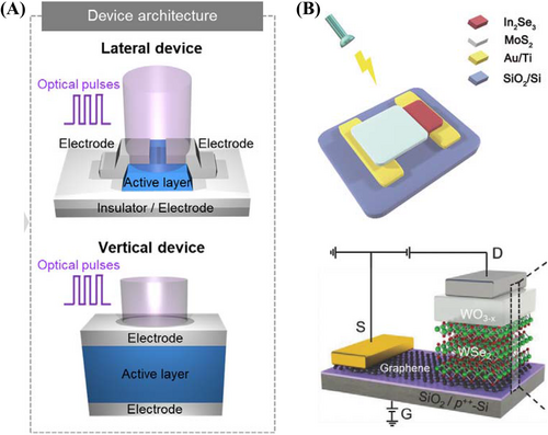
(A) Design of the lateral and vertical devices of optoelectronic synaptic devices. In Ref.91 Copyright © 2023 Minkyung Lee et al. Published by American Chemical Society. This publication is licensed under CC-BY 4.0. (B) Two-terminal and three-terminal devices. In Refs.27, 102 © 2023 Wiley-VCH GmbH. © 2018 WILEY-VCH Verlag GmbH & Co. KGaA, Weinheim.
| Structure | Heterostructure type | ON/OFF ratio | PPF index (%) | Energy consumption | Function | Reference |
|---|---|---|---|---|---|---|
| Two-terminal | Lateral In2Se3/MoS2 | 105 | – | – | Simulate the light adaptation behavior of the human-eye, and the EPSC can be tuned over a wide range | [102] |
| Two-terminal | Vertical MoS2/h-BN/graphene | 106 | – | – | Used as a multilevel nonvolatile optical memory device | [89] |
| Two-terminal | BP/CdS | – | – | 4.78 fJ for each training process | Image recognition | [88] |
| Two-terminal | Vertical (Al,Ga)N NW/graphene | – | 202 | 2.6 μJ for a single synaptic event | Spike-timing-dependence plasticity, spike-number-dependent plasticity, learning behavior, and the transition from STM to LTM | [103] |
| Three-terminal | Vertical SnSe/MoS2 | 103 | 20 | – | Simulate the human biological visual system, exhibits reversible resistive switching (RS) behavior | [104] |
| Three-terminal | Vertical Ag/WO3-x/WSe2/graphene | 105 | – | 0.1 nW for switching power | STP, LTP and PPF | [27] |
| Three-terminal | Vertical MoS2/PTCDA | – | 147 | 10 pJ for the acceptable power consumption | EPSC, PPF, IPSC, PPD, SRDP, etc. | [63] |
| Three-terminal | Vertical In2Se3/h-BN/CIPS | – | 170 | 6.9 pJ for per event | Pattern recognition, light adaptation, optical logic operation and event learning | [92] |
- Abbreviations: CdS, Cadmium sulfide; CIPS, CuInP2S6; EPSC, excitatory postsynaptic current; IPSC, inhibitory postsynaptic current; LTM, long-term memory; LTP, long-term plasticity; PPD, paired-pulse depression; PPF, paired-pulse facilitation; PTCDA, perylene-3,4,9,10-tetracarboxylic dianhydride; SRDP, spiking-rate-dependent plasticity; STM, short-term memory; STP, short-term plasticity.
3.4 Preparation methods
The ideal optoelectronic synapse is expected to have a fast response speed, low power consumption, a high signal-to-noise ratio, and the ability to simulate various synaptic functions such as STP, LTP, and spiking-timing-dependent plasticity. Achieving these functions depends on the efficient generation, transport, and recombination of photogenerated carriers within the device.16 The performance of optoelectronic synapses, especially those based on 2D material heterostructures, is significantly affected by the specific configuration of the heterostructure formed through the interaction of 2D materials.20
Currently, the main methods used to prepare 2D materials include both top-down peeling and bottom-up growth approaches. Top-down methods involve mechanical and solution peeling techniques. Mechanical peeling, which uses tape, and solution peeling, which involves reacting the sample with a solvent to extract a 2D film, are both fast and straightforward.18, 42 In contrast, the bottom-up growth method involves directly depositing materials onto a substrate to create 2D films. This method includes various techniques, such as molecular-beam epitaxy, CVD and metal organic chemical vapor deposition. These approaches offer the advantage of producing uniform and high-quality thin films over large areas.43 The fabrication of heterojunctions in 2D materials is mainly achieved through mechanical transfer stacking and epitaxial growth techniques. In the mechanical transfer stacking approach, 2D materials obtained through exfoliation are carefully layered onto another material with the assistance of a microscope. This method, known for being cost-effective and having minimal defect density, allows for the versatile integration of multiple 2D materials with different material compositions and stacking orientations.55 In contrast, epitaxial growth involves using a 2D material as a substrate to facilitate the growth of another material on top of it.55
Overall, further development and improvement of preparation processes are necessary to achieve the continuity and uniformity of 2D materials at larger sizes. Additionally, as the prepared 2D films must be transferred to the target substrates, it is imperative to ensure that the films remain intact and free of contamination during the fabrication of optoelectronic synaptic devices. Therefore, research on 2D material preparation methods and heterojunctions is significant for enhancing the performance of artificial synapses.105
4 APPLICATIONS
Optoelectronic synaptic devices can effectively regulate PSC and realize important functions such as STP and LTP.33, 53 In the biological nervous system, STP is responsible for quickly assessing and presenting information, while LTP is integral to the mechanisms of learning and memory.31 Moreover, there is potential to transform STM into enduring LTM.106 Optoelectronic synaptic devices combine the sensing capabilities of optical sensors with the ability to process and temporarily store visual information in real time.15 As a result, they offer promising applications in diverse fields such as image recognition, logical operations, and neuromorphic computing.
4.1 Image recognition
In traditional machine vision systems, there is a clear separation between the front-end image sensor and the back-end processor. The processor consumes significant energy and time in processing and recognizing the image data captured by the sensor.91 Optoelectronic synaptic devices offer a solution for emulating human visual functions and constructing machine vision systems through the creation of large-scale device arrays. These devices have the potential to streamline circuit design and reduce interconnection energy usage, thereby improving the overall efficiency of machine vision systems.6, 31, 90, 92, 107-109 For example, biological cone cells possess remarkable abilities to distinguish between strong light and colors, and they play a crucial role in the human visual system. Seo et al. integrated artificial synapses and light sensors onto the h-BN/WSe2 heterostructure, creating one artificial cone cell for every three neurons.29 Through this integration, they developed an artificial optical neural network (ONN) with 28 × 28 arrays, successfully simulating the color-mixed pattern recognition abilities of the human visual system.29 By performing pattern recognition tasks, such as identifying target numbers from color-mixed images and optimizing synaptic weights through training on various datasets, the ONN achieved a recognition rate of over 90%. This recognition rate was significantly higher than that of neural networks composed of synaptic devices that lacked optical sensing functions.
To further reduce the power consumption, Zhu et al. introduced a new approach to create an ultra-low power artificial photonic synapse. They achieved this by using a BP/Cadmium sulfide (CdS) heterostructure, with CdS as the photosensitive layer and BP as the channel layer. The device was used to build a three-layer fully connected optoelectronic neural network capable of recognizing Modified National Institute of Standards and Technology (MNIST) handwritten digits (Figure 6A). With an impressive image recognition accuracy of up to 94.1%, this device also has remarkably low energy consumption ranging from 0.43 to 8.9 fJ per light spike and 25 fJ per electrical spike.88
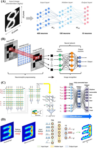
(A) Schematic illustration of the simulated FONN. In Ref. 88 Copyright © 2022, Chenguang Zhu et al. (B) ANN for image recognition. In Ref.110 Copyright © 2019, Feichi Zhou et al, under exclusive license to Springer Nature Limited. (C) Memristors for the fully connected CNN layers. In Ref.111 Copyright © 2023, Jongmin Lee et al. (D) Schematic illustration of the simulated SNN. In Ref.112 Copyright © 2023, Fakun Wang et al.
By using an artificial neural network (ANN), the neural morphological visual system can process visual data efficiently, similar to the visual cortex of the human brain. This system also reduces the amount of hardware and power consumption.110 Zhou et al. developed an image recognition system by utilizing a two-terminal optoelectronic resistive random access memory (ORRAM) synaptic device in ANN (shown in Figure 6B).110 The use of ORRAM preprocessing led to an impressive image recognition rate of 0.986, as demonstrated by the results. Yu et al. proposed a mechano-photonic artificial synapse based on a graphene/MoS2 heterostructure. The device consists of a heterojunction-based optoelectronic transistor and a triboelectric nanogenerator. The optoelectronic synaptic behavior, such as persistent photoconductivity, postsynaptic photocurrent, and photosensitivity, can be effectively controlled by manipulating the charge transfer/exchange between the graphene and MoS2 layers. They also simulated a three-layer ANN using the device to evaluate the impact of mechanical plasticity on image recognition accuracy. Through training, they discovered that the highest recognition accuracy could reach 92%. This type of mechano-photonic artificial synapse can easily be extended to multimodal sensory neurons, interactive photon synapses, artificial visual-somatosensory associative systems, and so on.52
Optoelectronic synapses can be integrated not only with ONN and ANN for image recognition but also with convolutional neural networks (CNN) and spiking neural networks (SNN). Lee et al. aimed to improve the accuracy of CNN image recognition by using a photoelectric synaptic array with color discrimination function (Figure 6C).111 Their experiment showed that the CNN, using its designed optoelectronic memristor (4-bit RGB image resolution), achieved an inference accuracy of approximately 94% (bidirectional) and 96% (unidirectional) when tested on the CIFAR-10 dataset. Additionally, the preprocessed input signal demonstrated a significant enhancement in RGB color resolution. Wang et al. employed SNN to evaluate optoelectronic devices based on the 2D b-AsP/MoTe2 vdW heterostructure (Figure 6D), and the inference accuracy of the MIR MNIST dataset encoded by the device exceeded 96%.112
Islam and his colleagues have developed an optoelectronic synaptic device that can detect, store, and manipulate optical data across a broad range of wavelengths, from UV to infrared. This allows for comprehensive optical information processing within the electromagnetic spectrum.113 As a result, this device is capable of constructing and recognizing multicolor patterns. To replicate the various functions of the human visual system, Zhang et al. developed a heterogeneous neuromorphic imaging system. This system is based on the concave hemispherical human retina and utilizes synaptic transistors with exceptional sensitivity.114 The system is composed of a 10 × 10 transistor array that transforms monochromatic radiation into stereoscopic light with different depths using prefabricated masks. This simulation mimics the 3D imaging behavior of the retina and demonstrates significant potential in the fields of visual restoration and artificial intelligence. Choi et al. constructed a curved neural morphology image sensor array based on a MoS2-organic heterostructure, which can achieve efficient image acquisition and recognition processes.115 This sensor array enables efficient image acquisition and recognition processes. By combining optoelectronic synaptic devices with various materials and structures in different neural networks, these devices can exhibit diverse performances, such as multiband light response, multicolor pattern recognition, and 3D imaging. These capabilities have promising applications in various fields.
4.2 Neuromorphic wearable electronic devices
Optoelectronic synaptic devices with neuromorphic computing capabilities have attracted considerable interest due to their potential application in wearable devices in the field of flexible electronics. 2D materials have been investigated for their thinness and impressive optoelectronic properties, making them excellent candidates for optoelectronic synaptic devices. These materials offer the potential for devices that are reliable, energy-efficient, and flexible.116-121 Additionally, optoelectronic synapses based on 2D materials enable the construction of wearable electronic devices with biocompatibility and portability.30
Visual injury receptors detect harmful stimuli or stimuli exceeding a certain intensity level. The optic nerve network then transmits pain signals to the cerebral cortex for advanced processing to avoid potential damage. Feng et al. successfully established a retinal-inspired artificial visual electronic skin with pain perception ability using flexible transistors. This innovative device can perform essential functions such as light response, memory retention, and visual pain calculation.122 Furthermore, it can execute painful photosensitization in various space–time color modes to prevent secondary visual damage (Figure 7A,B).122 After the activation of a visual nociceptor, the central nervous system receives, integrates, and transmits the pain information. Moreover, the skin of cephalopods serves as a flexible cognitive organ capable of perceiving, recognizing, and processing nerves in a distributed manner through complex biological processes. Leveraging this principle, creating an elastic and biaxially stretching device embedded with distributed neural and cognitive functions holds significant potential in fields such as skin repair surgery and wearable devices. Shim et al. utilized synaptic transistors made of elastic materials to develop a neural morphology recognition skin device. This device combines biaxial stretching and synaptic neural morphology functions to achieve image recognition, LTM retention, and fault tolerance.123 Therefore, the advancement of wearable electronic devices in intelligent healthcare can significantly promote the application of artificial electronic skin.
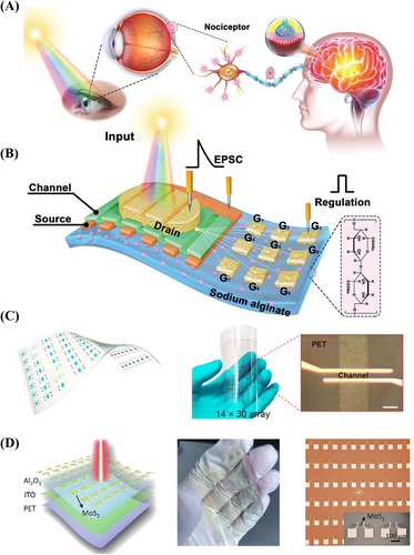
(A) Pathway of biological visual nociceptor. In Ref.122 © 2021 Wiley-VCH GmbH. (B) 3D device structure of a coplanar multiterminal flexible phototransistor network. In Ref.122 © 2021 Wiley-VCH GmbH. (C) Flexible Pyr-GDY/Gr/PbS-QD heterostructure-based optical synapse properties. In Ref.30 Copyright © 2021, American Chemical Society. (D) Devices made from MoS2 on a large scale and the magnified image of these devices. In Ref.125 Copyright © 2022, Tsinghua University Press.
Lee et al. successfully demonstrated optical wireless communication through the conversion of patterned optical stimuli into potential synaptic responses using organic optoelectronic artificial synapses. By assigning a distinct EPSC to each English letter, the device enables the generation of unique synaptic responses. Furthermore, when integrated with artificial muscle actuators, this device enables the development of an optical sensory neuromuscular electronic system, which presents a promising solution for enhanced optical wireless control of soft electronic devices.124 Hou et al. introduced a new two-terminal optical synapse that uses pyrenyl graphdiyne/graphene/PbS quantum dots. Interestingly, even when bent and folded, the LTP and LTD characteristics of these optical synapses remain mostly unchanged, showing great fault tolerance. The straightforward structure and low-dimensional properties of this synapse make it ideal for incorporation into wearable electronic devices (Figure 7C).30 Then, Li et al. fabricated optoelectronic synaptic devices on flexible substrates using MoS2 material through a simple gate modulation technique (Figure 7D).125 By using paired stimuli consisting of light and voltage pulses to integrate optoelectronic synapses and replicate the classical conditioned reflex Pavlovian dog experiment, they successfully achieved associative learning behavior. Hwang et al. conducted a study in which they created flexible artificial synapses with 2D heterojunctions. The results of their study showed that these synapses had excellent long-term enhancement and long-term cycling endurance on curved surfaces with a diameter larger than 10 mm or undergoing more than 700 bends.126 Additionally, the energy consumption per single peak was measured at 0.55 nJ. The researchers aimed to build a neural network and observed that the flexible synapses maintained a high level of recognition accuracy even under curved conditions. This promising outcome suggests a potential avenue for the advancement of wearable devices. Notably, the development of large-scale flexible optoelectronic devices highlights the potential application of human neuromorphic systems in wearable electronic products.
4.3 Logical operations
Using optoelectronic synaptic devices made of 2D materials, researchers have successfully performed logic operations by taking advantage of the changes in conductance caused by the frequency, quantity, and intensity of input stimuli.33 These capabilities make it possible to build large-scale computing systems and carry out computationally complex tasks with the help of collaborative optical inputs.30, 33
Hou et al. demonstrated optical logic functions that are modulated by inputting light pulses of different wavelengths, using optical synapses with vertical heterojunctions.30 In Figure 8A, signals A and B correspond to “0” and “1” for light off and on, respectively. To determine the logic function, modulation of the output current level is performed using the modulation input. The “OR” function is achieved when either input A or input B triggers it, surpassing the threshold, provided the modulation input is off. The “AND” function is attainable only when both inputs A and B are applied simultaneously, and the modulation input is activated, enabling the output current to surpass the threshold (Figures 8B,C). The “NOR” function is realized when either input A or B lowers the output current below the threshold once the modulation input is deactivated. Conversely, when the modulation input is activated and inputs A and B are applied simultaneously, the output current falls below the threshold, achieving “NAND.” Furthermore, the “XOR” function is achieved when the wavelengths of inputs A and B differ.
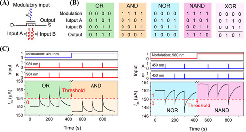
(A) Schematic diagram of optical synaptic logic function, (B) Logical operation table, and (C) current curves of logic functions. In Ref.30 Copyright © 2021, American Chemical Society.
In 2023, Fu et al. introduced a new type of dual-terminal photomemristor that consist of a graphene/MoS2-xOx/graphene structure.127 These devices are able to perform logic operations by responding to light, which is achieved through distinct memristor schemes involving electrical and optical stimulation. This approach includes a comprehensive logical framework that incorporates material implication and false operations.127 As a result, photomemristors can serve as both logic gates and storage units, enhancing the functional versatility of neural networks.
4.4 Neuromorphic computing systems
A neuromorphic computing system that can emulate the information processing functions of the human brain shows promise in addressing the bottleneck faced by conventional computing systems that use von Neumann architecture. This system takes advantage of the parallel operation of synapses, which serve as both computing and memory units, allowing for high-speed operation and low-power consumption in information processing.128-131 Synaptic devices are the fundamental elements in this neuromorphic computing paradigm, storing input information as electrical signals and processing data through synaptic weight updates.33 The amount of effective conductivity states, as well as the linearity and symmetry of weight update behaviors, are critical factors that influence the accuracy and reliability of recognition in neuromorphic computing.132 Optoelectronic neural synapses offer advantages such as low crosstalk and robust interconnections, making it easier to achieve neuromorphic computation.6, 133
Hou et al. implemented a three-layer ANN that included a hidden layer and utilized vertical heterojunction optical synapses.30 In this network, the synaptic weight is determined by the conductivity difference between two equivalent optical synapses. They used supervised learning to train the network on handwritten numerals sourced from the MNIST. To assess the network's fault tolerance, different levels of noise were introduced (Figure 9B). Remarkably, the network shows robust fault tolerance, maintaining an accuracy of over 80% even when subjected to a noise ratio of 60% (Figure 9C). Additionally, the network demonstrates the strong fault tolerance in both bent and folded states (Figure 9D,E).
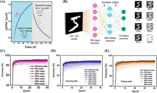
(A) LTP/LTD characteristic curve of light-stimulated synaptic transistors. In Ref.93 © 2022 Wiley-VCH GmbH. (B) Schematic diagram of a three-layer neural network for 28 × 28 pixel handwritten digit recognition. Handwritten digits with varying noise ratios (0−90%). (C) The network's recognition accuracies for handwritten digits with varying noise ratios in the flat state. The network's recognition accuracies for handwritten digits in the (D) bending and (E) folding states with different noise ratios. In Ref.30 Copyright © 2021, American Chemical Society.
Han et al. incorporated ultra-thin h-BN into graphene/CsPbBr3 quantum dots to serve as a carrier-regulating layer, thereby fabricating a three-layer heterostructure synaptic transistor.93 The application of continuous light pulses leads to a gradual increase in conductivity countered by a subsequent decline induced by continuous electrical pulses (Figure 9A). The two-layer neural network connected with this device achieves a recognition accuracy of approximately 91.5% for handwritten digits. This network comprises 10 output neurons, 300 hidden neurons, and 784 input neurons. The input image is converted into an output value through a weight matrix. Subsequently, the weight matrix is adjusted through backpropagation of the error between the output value and the image label value, thus enhancing the accuracy of digital recognition. Furthermore, Fang et al. developed a three-layer ANN that uses optoelectronic dual modulation of dual-terminal synaptic devices. They achieved a facial recognition accuracy of up to 95%.98 This highlights how the continuous improvement in recognition accuracy in neuromorphic computing systems is due to advancements in the materials and structures of optoelectronic synaptic devices.
Additionally, Li et al. developed a metal/semiconductor/metal (M/S/M) neuromorphic device using 2D metal sulfides as semiconductors. The goal was to create a convolutional neuromorphic network (CNN) for image processing and object detection.134 By controlling the concentration of sulfur ions in the M/S junction, the device can modify the height of the Schottky barrier. This modification is achieved by intentionally creating sulfur vacancies and controlling their movement with an electric field. Importantly, the M/S/M device can disrupt the symmetry of the electric potential, making the architecture for object position detection in neuromorphic vision networks simpler.
5 SUMMARY AND OUTLOOK
This review focuses on the use of heterostructures made from 2D materials in optoelectronic neuromorphic synaptic devices. By leveraging their unique properties, synaptic devices based on 2D materials demonstrate notable qualities in terms of learning ability, scalability, and efficiency. Despite significant progress in the application of 2D materials in artificial synaptic devices, there are still several technical challenges that need to be addressed before commercial applications can become a reality. First, it is crucial to have precise control over the growth of 2D materials in order to enhance structural uniformity and reliability. This is important for mitigating performance discrepancies among individual synaptic devices. Second, efforts to reduce device energy consumption and improve integration density are key areas of research. These efforts are essential for advancing artificial perception systems, wearable electronic devices, and computing systems that are based on neuromorphic technology. Furthermore, although current 2D-material-based synaptic devices primarily use light signals as input signals to regulate device performance, it is worth considering the use of light signals as response output signals as well. This could facilitate signal visualization. Further exploration is needed to investigate the application of 2D materials in multiterminal synaptic devices. This would enhance the capabilities of spatiotemporal information processing and provide new avenues for the dynamic simulation of the human brain.
In the future, the widespread adoption of optoelectronic neuromorphic synaptic devices requires continuous exploration and study. It is crucial to promote collaboration among researchers from different fields to effectively integrate knowledge in neurobiology, material preparation, device design, and neural networks. This collaborative effort aims to bridge the gap between artificial synaptic devices and biological synapses. By achieving a balance between low energy consumption and high stability, these devices can accurately simulate the neural networks of the human brain, enabling efficient and low-power brain-like computing. Moreover, the application scope of artificial synapses can be expanded by modifying the electrical band structure and the switching mechanism of synaptic devices through the creation of hybrid vdW heterostructures from combinations of 2D materials. Furthermore, the integration and interconnection of highly sensitive, low-power, and densely packed neuromorphic devices are crucial for advancing artificial perception systems, wearable electronic devices, and computing systems based on neuromorphic technology. This integration facilitates the seamless operation of these systems, enabling them to efficiently mimic the functionalities of the human brain while consuming minimal energy.
AUTHOR CONTRIBUTIONS
Yukun Zhao: Conceptualization; funding acquisition; methodology, project administration; supervision; visualization; writing—review & editing. Linrui Cheng: Formal analysis; investigation; methodology; resources; validation; visualization; writing—original draft; writing—review & editing. Rui Xu: Investigation; methodology; visualization; writing—original draft; writing—review & editing. Zexin Yu: Writing—review & editing. Jianya Zhang: Funding acquisition; project administration; supervision; writing—review & editing.
ACKNOWLEDGMENTS
This research was supported by the Key Research Program of Frontier Sciences, CAS (No. ZDBS-LY-JSC034), National Natural Science Foundation of China (No. 62174172), China Postdoctoral Science Foundation (Nos. 2023TQ0238 and 2023M742560) and Jiangsu Key Disciplines of the 14th Five-Year Plan (No. 2021135). The authors are grateful for the technical support for Nano-X, Platform for Characterization & Test from Suzhou Institute of Nano-Tech and Nano-Bionics, Chinese Academy of Sciences (SINANO).
CONFLICT OF INTEREST STATEMENT
The authors declare that they have no conflicts of interest.
ETHICS STATEMENT
Ethics approval was not needed in this study.
Open Research
DATA AVAILABILITY STATEMENT
Date sharing is not applicable to this article as no new data were created or analyzed in this study.


