Microstructures Formation by Fluorocarbon Barrel Plasma Etching
Abstract
The aim of our study is to generate microstructures in order to improve optical properties of monocrystalline silicon. By mean of fluorocarbon plasma barrel texturing and under certain process conditions, silicon turned black. As a result of silicon surface-plasma particles reactions, porous microstructures are formed, while a longer process time microspikes are developed. These microstructures are responsible of the high level of light trapping on almost the whole range of the usable portion of the solar spectrum. In the wavelength range of 400–1100 nm, the AM1.5G weighted reflection has been reduced to 6.20%. In addition to good trapping, this surface morphology leads to superior absorption, which is about 95% in the 600–1000 nm range and decreases to 36% at 1200 nm. This material is thus less transparent and absorbs near infrared light far more than the untreated silicon. Secondary ion mass spectrometry shows that elements from the ambient gas are deposited or superficially introduced into the silicon. In addition to surface texturing, these impurities are probably the reason of absorptance enhancement. Moreover, a pore formation mechanism is proposed.
1. Introduction
In photovoltaic, silicon texturisation is a technological operation which consists of an etching process to modify the morphology of the surface and improve its optical performance. The aim is to achieve the lowest light reflectance at the surface and highest light absorption particularly in the infrared region by generating randomly distributed microstructures on the surface such as micropyramids, spikes, or pores which trap the incident light [1–3].
Several techniques and methods were developed in order to obtain these various forms of microstructures. We can classify them in four main techniques; wet etching carried out in aqueous solution (alkaline, acidic, and electrochemical), laser-chemical etching, mechanical grooving, and dry plasma etching.
In the first technique, anisotropic alkaline etching is the most widely used method particularly in photovoltaic fabrication. However, this technique presents several disadvantages such as pollution, etched profile controlled by the crystal orientation and lowest surface reflectance limited to about 9% [4–7]. By mean of electrochemical formation of macropores, an average effective reflectivity of 10% is obtained [8].
The technique using a laser discharge in a gas is an innovation discovered accidentally at the University of Harvard in 1999 [3, 9]. A laser discharge in SF6 gas lead to a very low surface reflectance and an absorptance close to the unit (100%) in the wavelength range 1.2–2.5 μm. The explanation given to this phenomenon is related to the morphology of the surface as well as the presence of sulphide atoms which bind with the surface silicon atoms.
Mechanical texturing use different abrasive techniques like wire saw grooving, diamond scribing, and high rotational dicing blades. Depending on the method, the weighted reflectance varies from 3.5–5.7% [10].
Texturing silicon substrates can also be realized by means of plasma technology. It uses a gas flow discharge to dissociate and ionise molecules forming chemically reactive and ionic species. The chemistry is chosen such that these species react with silicon to form volatile products. The chemically reactive species or radicals that etch silicon are typically halogens of which the fluorine atom is the most effective one. Several equipments and process were developed for this purpose. This technique, initially used in microelectronic fabrication, was transferred to photovoltaic cells fabrication because it provides better improvements of the mechanical and optical characteristics than the wet technique [11]. With a remarkable reflectance of 1.4%, the parallel plate reactive ion etching (RIE) is the most widely spread etching system [12]. Texturing silicon with RIE can be performed in two ways. The first is to combine RIE with some kind of masking process such as lithography. The second is to use an automasking layer which under specific etches conditions allows the RIE process itself to create a random mask. This way is also known as the “black silicon method” developed by Jansen et al. [13]using a plasma gas mixture of SF6/O2/CHF3. Black silicon is formed when RIE etching is done on silicon with the etch conditions such that vertical walls are formed. Silicon turns black because the texture consists of long needles which trap the major incident light.
Silicon is also etched in cylindrical (barrel) reactor. This etching is predominantly chemical. The ions bombardment, responsible for the surface damage, is lower compared to the RIE process. Furthermore, barrel etcher operates at ambient temperature while RIE needs lower electrode temperature (less than 10°C). Another advantage of the barrel etcher is the higher loading of the wafers.
In this paper, we have investigated the possibility to microstructure silicon surface with CF4 + O2 plasma in the barrel type reactor usually used in photovoltaic fabrication of postdiffusion edge-junction isolation. This idea has emerged when we observed a blackening of the silicon wafer′s edge for certain plasma parameters. For a flat silicon surface, this blackening is really a texturisation. The morphology of the treated surface was modified with the formation of microcavities or micropores which trap the incident light, hence decreasing drastically light reflection and leading to a black surface. Compared to untreated silicon, this material is characterized by an important increase in light absorption in the range of 300–1200 nm not only due to the microstructures but also probably to impurities introduced into silicon or deposited on the surface during the etching process [9]. Moreover, the formation of the micropores can be explained by the same mechanism of the black silicon method.
2. Plasma Etching Process
When an RF power is applied between the two electrodes of the reactor, a discharge is established and the gas breaks down. The gas discharge contains atoms, radicals, positive and negative ions, electrons, and neutral species.
3. Experimental Details
The experiments were performed with the barrel plasma etching machine illustrated in Figure 1. It consists of two concentric perforated cages made of aluminium installed into the chamber process. The outer cage is the grounded electrode connected to chamber wall. The inner cage is the sample electrode to which RF power (13.56 MHz) is capacitively fed using a match box. The reactive gases CF4 + O2 are admitted using flow controllers from a gas manifold. A pressure of 50 mTorr in the etching chamber is achieved with a mechanical two-stage vacuum pump. The autopolarisation potential is about a few tens of volts (10–30 V). The process is then similar to a reactive ion etching (RIE) with lowions energies.
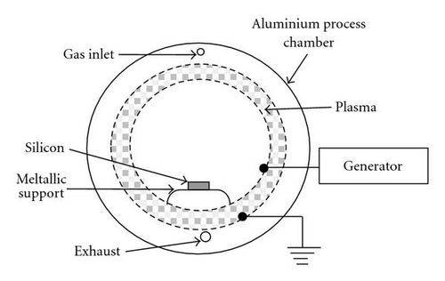
After cleaning, a monocrystalline silicon sample of 3 × 3 cm2 area is placed on a metallic support and positioned on the RF electrode.
As mentioned above, there is a borderline separation between plasma etching process parameters and polymer deposition process parameters [17]. So, the challenge is to choose correct plasma parameters leading to an etching process. A series of preliminary experiments allowed us to select parameters, ranges considered as the more likely to etch silicon. The following parameters have been tested: power 400 W, O2/CF4 gas rate mixture 8%, gas flow 15–30 sccm, chamber etching pressure 300–400 mTorr, and a chamber etching temperature ranging between 30–60°C.
In order to evaluate the impact of the texturing process, the total (specular and diffuse) hemispherical reflectance and transmittance were measured after etching using a Varian Cary 500 UV-VIS-NIR spectrophotometer equipped with an integrating sphere. The absorptance of the sample was then calculated from the relation A = 1−R−T. In addition to the optical properties, we used a CAMECA 4FE7 secondary ion mass spectrometer (SIMS) to characterize the chemical species formed during etching process and deposited onto the surface of the microstructures.
4. Results and Discussion
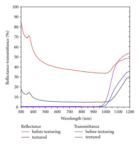
Decreases of the reflectance proportional to the processing time were measured after successive etchings. For a five-minute process, the textured surface exhibits a decrease of spectral reflectance between 5% and 15% in the wavelength range of 400–1100 nm. After 12 minutes of etching, the silicon surface appears almost black to the eye. The lowest reflectance was observed for a 15-minute process. (Figure 2, spectrum 2) represents the spectral reflectance of the so-called black silicon. It shows a broadband minimum around 5% for most of the usable portion of the solar spectrum. In the wavelength range 400–1100 nm, a weighted reflectance (Rw) of 6.20% has been achieved. Rw is the reflectance weighted by the solar spectrum AM1.5G. It also shows an almost uniform reflectance from 450–1000 nm. Compared to the untreated silicon surface which exhibits a weighted reflectance of 41.75% (Figure 2, spectrum 1), this kind of surface absorbs much more light.
The reduction of surface reflectance is due to the trapping of the major part of the incident light. Indeed, Figure 3a shows SEM images of a textured surface. We found out that the morphology is constituted of micropores of approximately 250 nm diameter and less.
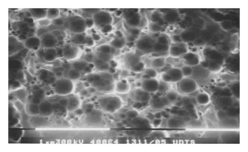
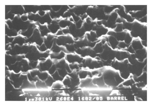
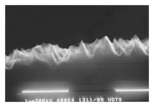
We choose the plasma parameters in a way that the micropore walls get almost completely etched, resulting in spike-like microstructures as shown in Figures 3(b) and 3(c). When the light strikes such a surface, it repeatedly bounces back and forth between these microstructure walls to dramatically reduce reflection. Figure 2 shows also the measured transmission spectra before (spectrum 3) and after texturisation (spectrum 4).
In the near-infrared region, the transmission is significantly lowered for texturised silicon. This material is therefore less transparent to the near-infrared light. Due to a decrease of both reflectance and transmittance, we do expect a light absorptance change.
Figure 4 shows the spectres absorptance of the silicon samples, obtained from the measured reflectance and transmittance data. On the whole range of the usable portion of the solar spectrum, we have observed an important absorption increase of 30–50% for the textured silicon surfaces compared to untreated silicon. As shown in spectrum 2, in the wavelength range of 600–1000 nm, an almost uniform broadband of 95% absorptance has been achieved whereas normal silicon, grey, and translucent absorbs less than 60% (spectrum 1).
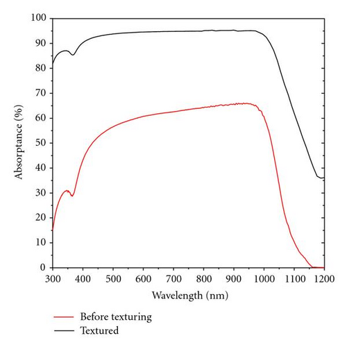
Since the band gap of crystalline silicon is about 1.1 eV, the absorption decreases sharply for wavelengths longer than 1000 nm as shown in Figure 3. The unmodified silicon surface does not absorb infrared light contrary to the textured surface which showed an increase in the near-infrared region. In other words, this material absorbs near-infrared frequencies that are transparent to ordinary silicon.
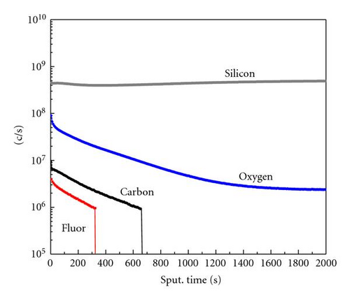
Absorptance enhancement in the visible, and near-infrared regions is accounted by both a drop in surface reflectance and a decrease of the transmittance through the textured silicon. Moreover, we think that this increase is not only due to the morphology of the microstructures but also to impurities introduced superficially into silicon or deposited onto the surface during the etching process. Indeed, as shown in Figure 5, depth analysis by SIMS reveals that a high concentration of the process gas constituents are present not only on the surface but also at a shallow depth, probably producing bands of impurity states in the band gap that can absorb infrared radiation. Concentrations of carbon and fluorine atoms, relatively high at the surface compared to silicon, decrease into the sample until they totally disappear. The high concentration of oxygen at the surface is due to the native oxide layer that grows on the surface after texturing.
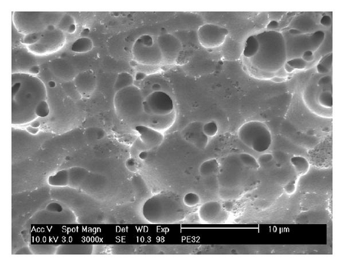
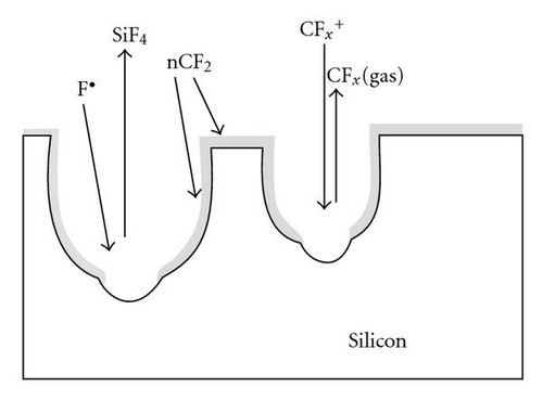
Due to the carbohalogen nature of the gas and relatively high process temperature (more than 30°C), the pores formation mechanism we propose is similar to the black silicon described in [13] except that the passivation layer is not the siliconoxyfluoride (SixOyFz) but fluorocarbon polymer film (nCF2). Figures 6 and 7 are, respectively, the SEM image showing the shape of the pores developed (nonoptimised process) and the scheme of pores formation mechanism proposed. Then, the CFx+ ions perforate the nCF2 passivating layer allowing to radical species F . to etch silicon. The by-products are, respectively, CFx (gas) and volatile SiF4.
5. Conclusion
In this article, we have shown the possibility to perform the texturisation of silicon in a barrel plasma reactor which is usually used in photovoltaic fabrication. The microstructures of the textured surface exhibits an important reflectance decrease due to trapping of the major part of the incident light. In the wavelength range 400–1100 nm, a weighted reflectance of 6.20% has been achieved. The absorptance spectra of the treated silicon samples over the whole range of the usable portion of the solar spectrum, show an important increase, of 30–50%. Furthermore, in the wavelength range of 600 nm to1000 nm, an almost uniform broadband of 95% absorptance has been achieved. This increase is not only due to the morphology of the microstructures but perhaps also to impurities introduced superficially into silicon or deposited onto the surface. We also proposed a mechanism of formation of the pores.
Acknowledgment
This work was supported by the Algerian Ministry of Scientific Research.


