Attaining 15.1% Efficiency in Cu2ZnSnS4 Solar Cells Under Indoor Conditions Through Sodium and Lithium Codoping
Abstract
The rising demand for sustainable low-power devices has driven interest in indoor photovoltaic (IPV) technologies for Internet of Things (IoT) applications. Composed of earth-abundant and non-toxic elements, Kesterite-based Cu2ZnSnS4 (CZTS) solar cells are highly attractive for IPV. This study systematically investigates the effects of sodium (Na), lithium (Li), and Na–Li co-doping on solution-processed CZTS devices. A comprehensive analysis reveals that Na-doping substantially improves crystallinity and grain morphology, significantly boosting efficiency, whereas Li alone has minimal impact. Notably, Na–Li co-doping achieves a 10.1% efficiency under AM 1.5G illumination, outperforming both the reference and singly doped devices. The co-doping synergy arises from Na-induced grain growth and Li-induced defect passivation and carrier concentration regulation. These devices exhibit high adaptability under 20 different indoor lighting conditions representative of real-world environments, achieving up to 15.1% power conversion efficiency under 3000 K illumination at 2.93 mW cm−2;—the highest reported indoor efficiency for CZTS cells. Their stable open-circuit voltage, high fill factor, and consistent efficiency across various color temperatures and intensities underline their suitability for IPV applications. Future work should focus on improving bandgap alignment with indoor light spectra to further enhance the efficiency of this eco-friendly technology for IoT energy solutions.
1 Introduction
The increasing demand for sustainable and eco-friendly energy solutions has accelerated advancements in photovoltaic (PV) technology, with the emerging field of indoor photovoltaics (IPV) gaining significant attention as a promising new focus in PV research.[1, 2] With the proliferation of Internet of Things (IoT) devices, wireless sensors, and other low-power electronics, the need for reliable energy harvesting from ambient indoor light sources—such as LEDs and fluorescent lamps—has become increasingly critical to reduce the reliance on disposable batteries and their associated environmental impact. Indoor PV systems, which convert artificial light or low-intensity scattered solar light into electrical energy, offer a promising solution to power these devices.[3] However, developing ideal IPV absorber materials and device architectures presents unique challenges due to the significantly lower irradiance levels and narrower wavelength spectrum indoors compared to outdoor sunlight.
To date, organic solar cells (OPVs), perovskite solar cells (PSCs), dye-sensitized solar cells (DSSCs), and silicon-based solar cells have been extensively explored for high-performance energy harvesting under indoor lighting conditions.[4] Among these, OPVs and PSCs have recently garnered significant attention for IPV applications, achieving efficiencies exceeding 30 and 42%, respectively, due to their ability to tune bandgap properties through donor–acceptor molecular design and compositional engineering.[5, 6] DSSCs have also demonstrated remarkable efficiency progress by sensitizers design, with reported efficiencies of up to 30.2% under indoor illumination.[7] However, these emerging technologies face challenges in operational stability, including thermal, photo, air, and mechanical degradation. Additionally, the presence of toxic chemical components in some of these technologies raises safety concerns, particularly for IPV devices integrated into IoT systems operating in close proximity to humans.[8, 9] Among the various material candidates for IPV, kesterite-based Cu2ZnSn(SxSe1–x)4 (CZTSSe) solar cells emerge as a promising solution due to their nontoxic and earth-abundant composition, tunable bandgap, and high absorption coefficients.[10] Their inorganic, environmentally friendly composition and excellent long-term stability make them particularly well suited for IPV applications. While the efficiency of kesterite solar cells under outdoor conditions (AM1.5G) has steadily increased in recent years,[11-15] exceeding 15%,[16] their potential under indoor lighting conditions remains largely underexplored.[17-19]
Compared to PV cells designed for standard outdoor conditions, IPV devices require careful consideration of two key factors: (1) alignment between the absorber layer's bandgap and the narrow spectral distribution of artificial light sources—typically around 1.7–2.0 eV for optimal photon energy utilization[20, 21]—and (2) high shunt resistance to minimize the impact of leakage currents on the open-circuit voltage (VOC) and fill factor (FF), usually degraded under low-light conditions.[17, 22] Previous studies have reported significant drops in VOC and FF when the illumination changes from standard outdoor conditions (AM1.5G) to low-intensity halogen lamp lighting for various kesterite-based materials such as CZTSe, CZTSSe, and CZTS, resulting in poor device performance.[17] This highlights the critical importance of bandgap alignment and shunt resistance management in designing efficient IPV devices. Pure sulfide kesterite (CZTS), with a typical bandgap (Eg) of ≈1.55 eV,[23] aligns with the spectral characteristics of indoor light sources, which predominantly emit in the visible range (380–740 nm). However, shunt resistance in CZTS solar cells is often compromised due to the presence of secondary phases, abundant point defects, unpassivated grain boundaries, severe interface recombination, and unfavorable morphology.[24] To overcome these challenges, recent research has focused on doping kesterite absorbers with extrinsic elements, particularly alkali elements such as sodium (Na), lithium (Li), and potassium (K).[25-27] These elements have demonstrated the ability to passivate defects, improve grain growth, and enhance the optoelectronic properties of the kesterite absorber.
It is well documented that relatively heavy alkali doping (e.g., Na, K) is beneficial for increasing the grain size of thin films and significantly improving morphology, while light alkali doping (e.g., Li) significantly enhances the carrier concentration and passivates the grain boundaries of the absorber.[25, 26, 28, 29] Na has been shown to significantly improve the crystallinity and grain morphology of kesterite films, promoting larger grains and reducing recombination losses at grain boundaries.[25, 26] This effect is attributed to the ability of Na to form low-temperature Na2Sex liquid phases, which act as fluxing agents and facilitate grain growth during annealing. Moreover, Li is known to enhance the performance of selenide (CZTSe) and sulfoselenide (CZTSSe) solar cells by passivating defects,[30, 31] forming downward band bending at grain boundaries,[32] and improving carrier concentration,[28] thereby boosting VOC, FF, and overall device efficiency. Recent studies have demonstrated that Li doping significantly improves the efficiency of CZTSSe solar cells due to the enhancement of carrier concentrations contributed by LiZn defect formation, creating beneficial shallow acceptor defects that enhance p-type conductivity.[28, 33] However, investigations into light alkali doping (Li) for sulfide kesterite (CZTS) remain scarce. The potential of Li doping to improve the optoelectronic properties of the absorber and enhance the efficiency of CZTS solar cells is still underexplored. Furthermore, codoping with heavy and light alkali is expected to synergistically improve grain morphology, increase carrier concentration, passivate grain boundaries, and mitigate detrimental defects, resulting in reduced recombination losses and significantly enhanced device performance.
In this study, we decoupled the effects of Na doping, Li doping, and Na–Li codoping on the film growth, grain morphology, optoelectronic properties, and final device performance of CZTS thin films. Through a series of detailed characterizations, we found that Na introduction significantly improved the grain size of the films, enhanced their optoelectronic properties, and improved device performance. In contrast, Li introduction alone had very limited positive effect on film morphology and optoelectronic properties. However, when both Na and Li were introduced, the device performance was further improved relative to Na doping alone. This enhancement stems from the synergistic effects of Li and Na, which not only enhance the crystalline quality of the films and yield larger grains but also effectively increase carrier concentration, passivate grain boundaries, and mitigate defects within the films. Consequently, the PV properties were significantly improved, leading to a CZTS solar cell with an efficiency of 10.1% under AM1.5G condition.
Furthermore, we explored the application of highly efficient Na–Li codoped CZTS solar cells for indoor PV applications, focusing on understanding their performance under different indoor lighting conditions. The devices were characterized under 20 different irradiation conditions, corresponding to five different color temperature light spectra (2700, 3000, 4000, 5000, and 6000 K) and four different irradiances (from 3 to 0.01 mW cm−2, from ≈10 000 to ≈100 lux), which are typically encountered in real-world indoor environments. Our results demonstrate a Na–Li codoped champion device with a PCE of 15.1% under 3000 K lighting and 2.93 mW cm−2 of irradiance. The high IPV efficiency of the device is attributed to its exceptionally high shunt resistance, which dominates the device's behavior under low light intensities by minimizing leakage currents and maintaining stable VOC and higher FF. While the current bandgap (1.55 eV) is not fully optimized for indoor light utilization, our findings suggest that enhancing grain growth, passivating defects, and improving carrier density through alkali codoping offer a promising pathway for optimizing CZTS materials for indoor applications. Future research should focus on fine-tuning the bandgap and further exploring the synergistic effects of alkali codoping to maximize the efficiency of IPV devices.
2 Results and Discussion
2.1 Effects of Alkali Doping on Kesterite Absorber Quality and Device Performance
The solution-processed Cu2ZnSnS4 (CZTS) solar cells were fabricated through three key steps: (1) precursor preparation: copper(I) chloride (CuCl), zinc acetate [Zn(OAc)2], and tin(IV) chloride pentahydrate (SnCl4·5 H2O) were dissolved in N,N-dimethylformamide to create the precursor solution; (2) spin-coating and annealing: the solution was spin-coated onto substrates and then annealed to form solid precursor films; and (3) chalcogenide atmosphere annealing: the films were annealed in a chalcogenide-rich atmosphere to promote crystallization and grain growth.[34, 35] Detailed methodologies are provided in the Experimental Section. To control Na diffusion, soda–lime glass (SLG) substrates with a SiOx barrier layer were used. Lithium perchlorate (LiClO4) and sodium perchlorate (NaClO4) were selected as alkali sources due to their solubility and thermal stability, as listed in Table S1, Supporting Information. High concentrations (0.5 m) of these alkalis were spin-coated onto the precursor films as top layers, as schematically illustrated in Figure 1a, thereby avoiding potential alterations of the precursor solution chemistry that could occur with alkali introduction into the solution. By introducing Na and Li, we systematically assessed their individual and combined impacts on device performance.
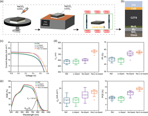
Figure 1b depicts the configuration of the CZTS solar cell, comprising a glass/Mo/CZTS/CdS/ITO structure. The representative current density–voltage (J–V) curves of the solar cells, shown in Figure 1c, reveal the substantial impact of different alkali doping strategies on device performance under standard AM1.5G illumination. Statistical box plots of the key PV parameters VOC, short-circuit current density (JSC), FF, and PCE are presented in Figure 1d, further highlighting the distinct improvements brought about by Na and Na–Li codoping. The reference (Ref.) device exhibits the poorest performance across all PV metrics, with a PCE of ≈6%. Upon Li doping, the device performance shows only modest improvement, indicating that Li doping alone does not significantly enhance CZTS performance. In contrast, Na doping leads to substantial improvements across all PV metrics, particularly in FF and PCE. This suggests that Na introduction significantly enhances charge carrier transport and reduces device resistance, likely due to improved crystallinity and larger grain size, which will be discussed in a later section. The most notable performance boost is observed with Na–Li codoping. The codoped device achieves the highest values for VOC (722 mV), JSC (23.4 mA cm−2), FF (59.3%), and PCE (10.1%). Specifically, the Na–Li codoped CZTS device demonstrates an increase in VOC due to the increase the carrier concentration, reduced nonradiative recombination, and potential grain boundary passivation, which will be discussed in detail in the following section. The FF is improved as a result of reduced series resistance and enhanced charge carrier transport, benefiting from the synergistic effects of both Na and Li. Consequently, the PCE is elevated from 6.4% in the Ref. device to 10.1% in the Na–Li codoped device, representing a significant overall efficiency enhancement.
The external quantum efficiency (EQE) spectra (Figure 1e) provide further insights into the impact of alkali doping on the optical and electronic properties of the CZTS devices. The Ref. device exhibits a broad EQE response peaking between 500 and 700 nm, corresponding to an Eg of ≈1.55 eV, but with lower overall EQE values compared to the alkali-doped devices, indicating higher recombination losses and less efficient photon–electron conversion. Li doping results in a modest improvement in EQE, suggesting slight enhancement in charge collection efficiency. In contrast, Na doping significantly improves the EQE across the 500–900 nm range, indicating reduced recombination losses. The slight reduction in bandgap to 1.53 eV further supports enhanced light harvesting, particularly in the near-infrared region. The Na–Li codoped device achieves the highest EQE across the spectrum, demonstrating that the codoping strategy minimizes recombination and maximizes charge collection by improving absorber quality, resulting in superior overall device performance. The Urbach energy (EU) was derived from the EQE data (Figure S1, Supporting Information). The Ref., Li-doped, and Na-doped samples exhibit similar EU values around 38 meV, indicating comparable levels of band tailing. However, the Na–Li codoped sample shows a lower EU of 34 meV, suggesting reduced band tail states associated with defects such as CuZn and [2CuZn + SnZn].[36, 37] This reduction suggests that Li helps suppress detrimental defects, which directly contributes to the improved VOC and PCE of the device. The lower EU in the Na–Li codoped sample highlights the effectiveness of codoping in enhancing absorber quality and overall device performance.
To understand the mechanisms underlying the performance enhancements observed with different alkali doping strategies, we conducted detailed analyses of the films before and after sulfurization using X-ray diffraction (XRD), Raman spectroscopy, and scanning electron microscopy (SEM). The XRD patterns of the precursor films (Figure 2a) display diffraction peaks which correspond to the (211), (204), and (312) planes of the kesterite phase. Their broad width and weak intensity are indicative of a low-crystallinity kesterite structure. Notably, no secondary phases are observed in the precursor films, suggesting a pure kesterite composition free from impurities. Additionally, no peaks corresponding to NaClO4 or LiClO4 are detected, implying that these compounds, if present, are likely amorphous and reside on the film surface. Raman spectroscopy (Figure 2d) complements the XRD findings by confirming the presence of low-crystallinity kesterite phases in the precursor films. In the Na–Li codoped films, vibrational peaks attributed to (ClO4)−1 at around 930 cm−1 are detected, indicating the presence of these compounds on the film surface. This suggests that the alkali salts remain on the surface in an amorphous state after spin-coating and before sulfurization. Additionally, the presence of LiClO4 and NaClO4 on the film surface is further confirmed by SEM image shown in Figure S2, Supporting Information.
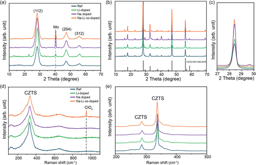
It has been previously reported that low-crystallinity kesterite films undergo a direct, single-phase transformation from an amorphous kesterite structure to a highly crystalline absorber layer during heat treatment in a chalcogenide atmosphere (S or Se).[35, 36, 38] This transformation pathway avoids the formation of secondary phases and is critical for preparing high-quality kesterite films. Our findings are consistent with this mechanism. After sulfurization, the XRD patterns of the absorber layer films (Figure 2b) reveal a significant improvement in crystallinity. The characteristic peaks of kesterite become sharper and more intense, indicating larger grain sizes and enhanced crystal ordering. Notably, the Na-doped and Na–Li codoped films exhibit stronger diffraction peaks with narrower full width at half maximum (FWHM) values, as shown in the zoomed (211) peak (Figure 2c). This observation suggests that Na plays a crucial role in promoting grain growth and improving crystallinity. In contrast, the Li-doped films do not show significant enhancement in crystallinity; the diffraction peaks remain relatively broad and weak compared to the Na-doped and Na–Li codoped films. As mentioned above, this aligns with previous studies indicating that Na facilitates the formation of a Na2Sx liquid phase during sulfurization, which acts as a flux to promote grain growth and improve crystal quality.[39] Raman spectroscopy of the absorber films (Figure 2e) further corroborates the XRD results. The Raman spectra reveal distinct peaks at 285 and 330 cm−1, associated with kesterite CZTS, with no detectable secondary phases such as ZnS or SnS. The absence of secondary phases in both XRD and Raman analyses emphasizes the effectiveness of Na doping in enhancing crystallinity without introducing unwanted compounds.
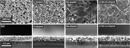
SEM images presented in Figure 3 further illustrate the significant impact of alkali doping on the grain morphology of CZTS thin films. The Ref. film exhibits small, irregular grains with numerous grain boundaries, likely serving as recombination centers that limit device performance. This observation aligns with the poor crystallinity indicated by the broad and weak peaks in the XRD patterns and correlates with the low-efficiency metrics of the Ref. devices. The Li-doped film shows only minor improvements in grain size and morphology compared to the Ref. The SEM images and XRD patterns of the Li-doped film remain similar to those of the Ref., suggesting that Li alone does not significantly improve crystallinity or promote grain growth. In contrast, the Na-doped film displays much larger, well-defined grains with reduced grain boundary density, as evidenced by the SEM images. This improved grain morphology corresponds with sharper and more intense peaks in the XRD patterns, indicating enhanced crystallinity and larger grain sizes. The larger grains and fewer grain boundaries lead to decreased recombination and improved charge transport, resulting in significant enhancements in device parameters such as JSC, FF, and PCE. The Na–Li codoped film exhibits grain morphology similar to that of the Na-doped film, with no significant further improvement in grain size or uniformity observed in the SEM images. Despite the similar crystal morphology, the Na–Li codoped films demonstrate better optoelectronic properties compared to the Na-doped films.
To analyze the depth distribution of elements within the films and understand the effects of Na and Li incorporation, we employed glow discharge optical emission spectroscopy (GDOES). The results, shown in Figure S3a–e, Supporting Information, indicate that the primary kesterite elements—Cu, Zn, Sn, and S—are uniformly distributed throughout the depth in each sample. A clear Na signal is present in the Ref. sample, suggesting that despite the application of a SiOx layer beneath the Mo as a Na diffusion barrier (Figure 1b), Na migration from the substrate into the CZTS layer still occurs at the high annealing temperature of 640 °C. However, this substrate-derived Na did not significantly enhance film morphology, likely due to its low concentration. So, Na diffusing from the SLG does not dominate the absorber quality enhancement. In the Na-doped samples (Na-doped and Na–Li codoped), the Na signal is significantly stronger, indicating successful incorporation of Na from the spin-coated NaClO4 layer. Interestingly, in the Li-doped samples (Li-doped and Na–Li codoped), almost no Li is detected, while the Na content is notably higher than in the samples without Li (Figure S3e, Supporting Information). GDOES analysis of the precursor film (Figure S3f, Supporting Information) confirms a substantial Li presence on the film surface before sulfurization, indicating that Li is not lost during the spin-coating process.
Yang et al. previously reported on the competitive exchange behavior between Na and Li in kesterite films, where Na tends to repel Li from the film and their interaction promotes Na diffusion.[40] This phenomenon explains the consistent observation of significant Li loss during experiments. Our study aligns with this mechanism, showing that Na repels Li during the high-temperature sulfurization process, leading to severe Li depletion and its undetectability via GDOES in the final films. This Na–Li exchange mechanism results in Li effectively enhancing the Na content within the film, as illustrated in Figure S3e, Supporting Information.
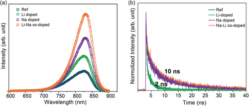
Photoluminescence (PL) and time-resolved PL (TRPL) measurements were conducted to elucidate the role of alkali doping in enhancing the optoelectronic properties of CZTS devices (Figure 4). The Ref. sample exhibits the weakest PL intensity and the shortest carrier lifetime (≈2 ns), indicating a high density of recombination centers. This high recombination rate leads to poor charge collection and low device performance, consistent with the inferior PV metrics observed. Li doping results in a slight increase in PL intensity, reflecting modest improvements in reducing recombination losses. However, the overall effect on device performance remains limited, aligning with the minimal enhancements observed in the J–V characteristics. In contrast, Na doping significantly enhances PL intensity and extends the carrier lifetime to ≈10 ns. The increased PL intensity and carrier lifetime indicate improved absorber quality and reduced nonradiative recombination, likely due to enhanced crystallinity and fewer grain boundaries facilitated by Na incorporation, which correlates with better device performance. The Na–Li codoped device exhibits the highest PL intensity among all samples studied, indicating a further reduction in recombination. This enhanced PL behavior is attributed to the synergistic effect of Na and Li codoping. The introduction of Li alongside Na likely promotes the formation of beneficial shallow defect states such as LiCu, LiZn, and VCu, which enhance p-type conductivity and help passivate detrimental defects and grain boundaries of absorber, as supported by DFT calculations.[28, 33, 41]
Alkali doping is known to increase the carrier concentration for the kesterite, thereby improving overall device performance. To quantify this effect, capacitance–voltage (C–V) measurements were performed, and the results are presented in Figure S4, Supporting Information. The Ref. and Na-doped devices exhibit similar carrier concentrations, around 2 × 1016 cm−3. However, Na–Li codoping significantly increases the carrier concentration to ≈6 × 1016 cm−3. This substantial increase in carrier concentration can be attributed to two primary factors, as reported in both DFT and experimental literature: 1) formation of shallow acceptors: the incorporation of Li into the film leads to the formation of shallow acceptor defects such as LiCu and LiZn,[21, 26, 34] enhancing p-type conductivity; 2) assisting Na incorporation: Li facilitates a higher Na content within the film, as observed in the GDOES analysis. The increased Na content promotes the formation of beneficial copper vacancies (VCu), further improving carrier density.[42]
2.2 Efficient CZTS Solar Cells for IPV Applications
As mentioned before, for optimal performance in indoor conditions, the IPV device needs to meet two key criteria: (1) a bandgap of 1.7–2.0 eV to match the typical indoor light spectra,[21] and (2) high shunt resistance to minimize leakage currents, which become the dominant source of carrier losses under low-light conditions.[43] In this study, the champion CZTS device features an absorber layer with a bandgap of 1.55 eV. Although this is somewhat lower than the ideal value for IPVs, it demonstrates the potential for further performance improvement through bandgap tuning.
Our results demonstrate that high-efficiency CZTS solar cells exhibit remarkable adaptability and efficiency under varying lighting conditions, including both simulated sunlight (AM1.5G) and artificial indoor lighting. Figure 5a shows the J–V curve of the champion CZTS device under AM1.5G illumination and dark conditions. The device displays a high shunt resistance (≈10 000 Ω cm2), which is ideal for indoor PV applications. The device's response to varying light intensities under the AM1.5G spectrum is shown in Figure 5b. As the light intensity decreases from 1 to 0.1 sun, the FF improves from 59.1 to 67.1%, with only a slight reduction in VOC. The stability of VOC across these intensities indicates that the device effectively minimizes carrier recombination losses. This demonstrates that CZTS solar cells efficiently harvest energy under low-light conditions, such as scattered sunlight commonly found indoors during the day.
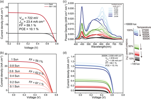
Figure 5c provides spectrum for 20 different indoor lighting conditions used to characterize device performance in this study, including five color temperature lights (2700, 3000, 4000, 5000, and 6000 K) and four intensity levels for each temperature light. We used this wide range of spectra for performance testing, rather than a single-color temperature and illumination intensity, to accurately evaluate the real-world performance of solar cells under complex lighting conditions and to simulate the device's operation in realistic indoor environments. Figure 5d presents the J–V curves under the various indoor lighting conditions depicted in Figure 5c. The device maintains high FF values under most of these conditions, and although VOC shows a slight drop compared to 1 sun illumination, the overall efficiency remains high; the PV parameters are detailed in Table 1 and Table S2, Supporting Information. Under specific conditions, particularly those with high intensities near the light source and warm color temperatures (e.g., 2700 and 3000 K), the CZTS device achieves a PCE of up to over 15.0%, highlighting its potential for indoor PV applications. The slight decrease in VOC under low-light conditions is consistent with the expected influence of light intensity on VOC; however, the higher FF values help to maintain a high PCE overall.
| Illumination | Incident power [mW cm−2] | Illuminance [lux] | V OC [mV] | J SC [mA cm−2] | FF [%] | PCE [%] |
|---|---|---|---|---|---|---|
| 2700 K-100% | 3.157 | 10 248 | 616.2 | 1.14 | 67.7 | 14.97 |
| 2700 K-50% | 1.306 | 4240 | 585.5 | 0.49 | 67.7 | 14.64 |
| 3000 K-100% | 2.938 | 9586 | 619.2 | 1.06 | 68.1 | 15.06 |
| 3000 K-50% | 1.158 | 3778 | 585.7 | 0.44 | 67.4 | 14.57 |
| 4000 K-100% | 2.884 | 9256 | 618.1 | 1.03 | 67.9 | 14.83 |
| 4000 K-50% | 1.131 | 3630 | 584.5 | 0.43 | 67.3 | 14.49 |
| 5000 K-100% | 2.916 | 9440 | 621.2 | 1.04 | 68.2 | 14.87 |
| 5000 K-50% | 1.157 | 4720 | 587.8 | 0.43 | 67.5 | 14.57 |
| 6000 K-100% | 2.638 | 7790 | 617.2 | 0.94 | 67.5 | 14.70 |
| 6000 K-50% | 1.003 | 3746 | 582.2 | 0.37 | 66.4 | 14.25 |
| AM1.5G | 100.0 | n/a | 722.0 | 23.4 | 59.3 | 10.1 |
Figure 6 displays filled contour plots for VOC, JSC, FF, and PCE across the range of tested indoor lighting conditions. These plots illustrate the strong performance of CZTS solar cells under most conditions. As shown in Figure 6a, the device maintains a stable VOC across various color temperatures and intensities, indicating effective charge separation and low recombination rates. The JSC plot in Figure 6b reflects the device's capability to maintain decent current generation even as lighting conditions vary. In terms of FF (Figure 6c), the device consistently achieves values above 65% under moderate to high light intensities across all color temperatures, confirming the beneficial effects of high shunt resistance. This behavior contrasts sharply with previous reports on kesterite solar cell under low-light condition, including CZTSe, CZTS, and CZTSSe, which exhibited significant drops in VOC and FF compared to AM1.5G illumination, as summarized in Table S2, Supporting Information. This resilience against changes in lighting conditions makes CZTS solar cells particularly well suited for indoor applications, where they may be exposed to a variety of artificial and natural light sources. Finally, the PCE plot (Figure 6d) reveals that the CZTS device achieves efficiencies exceeding 14.5% under most lighting conditions, with peak performance around 15.0% under 3000 K at 100% intensity (2.93 mW cm−2, 9586 lux), closely resembling conditions near the light source. This level of efficiency is promising for indoor PV applications aimed at powering IoT devices.
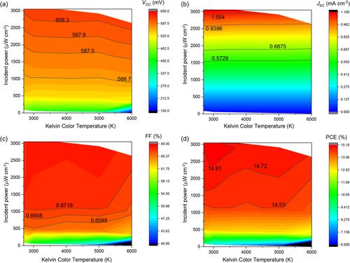
This comprehensive testing illustrates the versatility of CZTS solar cells in adapting to various light sources typically found indoors, such as LEDs, fluorescent lamps, halogen lamps, and even indirect sunlight. Notably, the performance remains robust across all conditions, underscoring the potential of CZTS solar cells for indoor applications where light sources can vary significantly in intensity and spectral distribution, such as rooms that receive both artificial light and scattered sunlight.
Building on the promising efficiency of CZTS solar cells under indoor lighting, we evaluated their practical application in powering commercial IoT devices—device 1: Philips Hue Motion Sensor, device 2: Pressac CO2 Temperature & Humidity Sensor, and device 3: Honeywell HIH6130 Temperature & Humidity Sensor—each with varying power demands of 0.02, 0.12, and 0.28 mW cm−2, respectively, under indoor illumination. Detailed simulations regarding the powering of devices 1–3 are summarized in the Supplementary Information. Figure 7 illustrates the power generation density (PGD) of the CZTS solar cell under 3000 K lighting and its comparison with the power consumption density (PCD) of the IoT devices. The shaded yellow area represents the expected indoor light intensity range, between 0.3 and 3 mW cm−2, which is typical for artificial lighting in indoor environments.
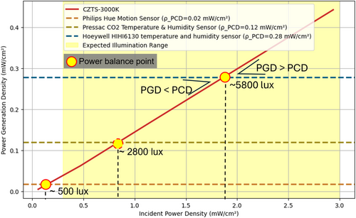
In this simulation, the PGD line intersects with the PCD requirements of each IoT device, revealing the minimum light intensities needed for each device to function. For IoT Device 1, which requires 0.02 mW cm−2 to operate, the PGD exceeds the PCD across the entire indoor light intensity range. This indicates that the CZTS solar cell can effectively power this device even under very low-illumination conditions, with sufficient energy to meet the device's operational needs and potentially store excess energy. IoT devices with higher power demands, such as device 2 (0.12 mW cm−2) and device 3 (0.28 mW cm−2), require more intense illumination to reach the power balance point where PGD equals or surpasses PCD. For device 2, this threshold is ≈0.8 mW cm−2, while for device 3, it is around 1.85 mW cm−2. Thus, device 2 can operate in moderately low indoor lighting, whereas device 3 requires more intense lighting—such as direct exposure to indoor LEDs—to function reliably.
These results demonstrate that the high efficiency of CZTS solar cells in indoor settings enables them to produce a sufficient amount of electrical energy, meeting the operational power requirements of various IoT devices. This adaptability to diverse indoor lighting conditions confirms CZTS solar cells as a promising technology for sustainable, self-powered IoT systems. Furthermore, the analysis provides a clear framework for determining the conditions under which CZTS solar cells can power specific devices, emphasizing their potential to drive low-power IoT networks in controlled environments like smart homes and offices.
3 Conclusion
This study demonstrates that Na–Li codoping significantly enhances the performance of solution-processed CZTS solar cells. The codoped devices achieved a PCE of 10.1% under standard AM1.5G illumination and an impressive 15.1% under indoor lighting conditions (3000 K, 2.93 mW cm−2), which is the highest reported efficiency for CZTS solar cells in indoor environments to date. The enhanced performance is attributed to the synergistic effects of Na and Li codoping: Na promotes grain growth and reduces recombination at grain boundaries, improving charge transport, while Li increases carrier concentration and passivates defects, leading to higher VOC and FF. The codoped CZTS solar cells exhibited exceptional adaptability under various indoor lighting conditions, maintaining high FF and stable VOC across a range of color temperatures and light intensities. This adaptability underscores their suitability for IPV applications, particularly in powering low-power electronics like IoT devices.
These findings highlight Na–Li codoping as an effective strategy to optimize CZTS solar cells for both outdoor and indoor applications. The approach leverages the individual benefits of each dopant to achieve significant improvements in device efficiency. Future research should focus on bandgap engineering to better align the absorber properties with indoor light spectra, potentially targeting an optimal bandgap range of 1.7–1.9 eV. These efforts could involve exploring alloying strategies within the kesterite family to further enhance device efficiency under indoor conditions. This work offers a promising pathway for advancing CZTS solar cells as efficient, nontoxic, and earth-abundant PV technologies suitable for sustainable energy solutions in indoor environments. The success of this codoping strategy paves the way for the development of high-performance IPV kesterite devices, contributing to the growing demand for clean energy sources in powering next-generation electronics.
Acknowledgements
This project received funding from the European Union's H2020 research and innovation program under grant agreement number 866018 (SENSATE) and by the Science Ministry of Spain projects number PID2023-148976OB-C41 (CURIO-CITY). The authors from UPC belong to the Micro and Nanotechnologies for Solar Energy Group (MNT-Solar) Consolidated Research Group of the “Generalitat de Catalunya” (2021 SGR 01286). Y.G. thanks the European Union's Horizon 2020 research and innovation program under the Marie Skłodowska-Curie grant agreement no. 10115148. R.S. thanks FWO for the funding through the Fundamental Research Ph.D. Fellowship (1178024N) and Travel Grant for a long stay abroad (V462623N). D.P. and A.P. thank projects SCALING (PID2022-138434OB-C52) and InnoPV (PID2022-140226OB-C31) funded by MCIN/AEI/10.13039/501100011033/ FEDER, UE. S.G. thanks the Serra Húnter program. M.P. thanks InnoPV (PID2022-140226OB-C32) funded by MCIN/AEI/10.13039/501100011033/ FEDER, UE. Z.J. thanks financial support from Spanish Ministry of Science, Innovation through the Ramon y Cajal fellowship (RYC2021-033239-I). E.S. is grateful to ICREA Academia program.
Conflicts of Interest
There are no conflicts to declare.
Author Contributions
Edgardo Saucedo: conceptualization (equal); funding acquisition (lead); methodology (supporting); resources (lead); supervision (lead); validation (equal); writing—original draft (supporting); writing—review and editing (lead). Yuancai Gong: conceptualization (lead); data curation (lead); formal analysis (lead); funding acquisition (supporting); investigation (lead); methodology (lead); supervision (supporting); validation (equal); writing—original draft (lead); writing—review and editing (equal). Alex Jimenez-Arguijo: data curation (supporting); formal analysis (supporting); investigation (supporting); visualization (supporting); writing—original draft (supporting); writing—review and editing (supporting). Ivan Caño: formal analysis (supporting); investigation (supporting); methodology (supporting); writing—review and editing (supporting). Romain Scaffidi: conceptualization (supporting); data curation (supporting); formal analysis (supporting); investigation (supporting); methodology (supporting); writing—review and editing (supporting). Claudia Malerba: data curation (supporting); formal analysis (supporting); investigation (supporting); validation (supporting); writing—original draft (supporting); writing—review and editing (supporting). Matteo Valentini: data curation (supporting); formal analysis (supporting); investigation (supporting); writing—review and editing (supporting). David Payno: data curation (supporting); formal analysis (supporting); investigation (supporting); writing—review and editing (supporting). Alejandro Navarro-Guell: data curation (supporting); investigation (supporting); writing—review and editing (supporting). Oriol Segura-Blanch: data curation (supporting); investigation (supporting); writing—review and editing (supporting). Denis Flandre: conceptualization (supporting); investigation (supporting); methodology (supporting); resources (supporting); supervision (supporting); validation (supporting); writing—review and editing (supporting). Bart Vermang: conceptualization (supporting); funding acquisition (supporting); investigation (supporting); methodology (supporting); resources (supporting); supervision (supporting); validation (supporting); writing—review and editing (supporting). Alejandro Perez-Rodriguez: funding acquisition (supporting); methodology (supporting); resources (supporting); writing—review and editing (supporting). Sergio Giraldo: formal analysis (supporting); investigation (supporting); methodology (supporting); writing—review and editing (supporting). Marcel Placidi: conceptualization (supporting); funding acquisition (supporting); investigation (supporting); resources (supporting); writing—review and editing (supporting). Zacharie Jehl Li-Kao: conceptualization (supporting); data curation (supporting); formal analysis (supporting); investigation (supporting); methodology (supporting); software (lead); writing—review and editing (supporting).
Open Research
Data Availability Statement
The data that support the findings of this study are available from the corresponding author upon reasonable request.


