Enhanced Electrostatic Dust Removal from Solar Panels Using Transparent Conductive Nano-Textured Surfaces
Abstract
Dust accumulation on solar panels is a mjor operational challenge faced by the photovoltaic industry. Removing dust using water-based cleaning is expensive and unsustainable. Dust repulsion via charge induction is an efficient way to clean solar panels and recover power output without consuming any water. However, it is still challenging to remove particles of ≈30 µm and smaller because Van der Waals force of adhesion dominates electrostatic force of repulsion. Here, the study proposes nano-textured, transparent, electrically conductive glass surfaces to significantly enhance electrostatic dust removal for particles smaller than ≈30 µm. We perform atomic force microscopy pull-off force experiments and demonstrates that nano-textured surfaces reduce the force of adhesion of silica micro-particles by up to 2 orders of magnitude compared to un-textured surfaces from 460 to 8.6 nN. We show that reduced adhesion on nano-textured surfaces results in significantly better dust removal of small particles compared to non-textured or micro-textured surfaces, reducing the surface coverage from 35% to 10%. We fabricate transparent, electrically conductive, nano-textured glass that can be retrofitted on solar panel surfaces using copper nano-mask based scalable nano-fabrication technique and shows that 90% of lost power output for particles smaller than ≈10 µm can be recovered.
1 Introduction
Most of the large solar power plants of capacity >500 MW are in dry geographic regions such as deserts due to the availability of sunlight and land. However, there is significant wind and airborne dust in these regions which accumulates on top of the panels over time, blocking the incident sunlight.[1-6] Solar panels have to be cleaned regularly to maintain the power output.[1, 7-9] Water-based cleaning, which is the most widely used cleaning method is expensive and contributes to up to 10% of annual operation and maintenance cost.[1, 10] Further, water-based cleaning techniques are unsustainable due to the large freshwater footprint of >10 billion gallons per year.[11] Waterless brush scrubbing introduces irreversible scratching damage that affects the long-term operation of solar panels.[12] Alternate effective cleaning methods can therefore significantly transform the photovoltaic solar power industry.
Since the dielectrophoretic force is a weak, short-range force, it is challenging to remove dust particles with a diameter smaller than 100 µm.[21] Therefore, in our previous work we engineered an active coulombic charge induction-based dust removal system for significantly more effective electrostatic dust removal[11] compared to electrodynamic screens.
The Coulombic force FE (Equation (2)) is a function of the particle diameter D, the vacuum permittivity ɛ0, the relative permittivity of the surrounding medium ɛr,m = 1, i.e., air, and the electric field strength E which is limited by the electrical breakdown of air at Emax ≈ 3 MV/m.[22] The previously specified conditions yield FE ≫ FDEP for all dust particle sizes. Especially for decreasing particle size FE grows more rapidly compared to FDEP as FE D2 and FDEP D3. However, even in active charging system, as the particle diameter approaches the range of 20–40 µm and lower, it is challenging to remove them electrostatically.[11]
FE is counteracted by the gravitational force Fg = πρD3/6 acting on the silica particle with typical density ρ ≈ 2650 kg m−3. Comparing Fg with FE yields Fg ≪ FE for D < 1 mm and hence gravity can be neglected. Further, the electrostatic force of repulsion is counteracted by force of adhesion FA (Figure 1C). The primary mechanisms for particle adhesion to a solid surface are Van der Waals attraction, capillary condensation of water vapor at the particle-surface interface, and electrostatic forces due to tribo-electrically charged particles and surfaces.[23] In studies without either capillary condensation or significant tribo-charging, the only mechanism for particle adhesion is Van der Waals attraction force which scales with the particle diameter (,[24-26] where A ≈ 6.3 × 10⁻²⁰ J (for silica in air) is the Hamaker constant and d0 ≈ 0.4 nm the atomic separation between particle and surface.[11] As FA > FE for D < 100 µm and FA/FE 1/R, Van der Waals force increasingly dominates electrostatic force of repulsion for decreasing particle diameter and makes it challenging to remove them from the electrode surface. Electrostatic force for a certain particle diameter is limited by Emax = 3 MV/m. Figure 1A shows the electrostatic removal of large particles (≈327 µm) almost completely from the surface of a silicon wafer electrode after the application of voltage. Here the applied voltage is ≈15 kV between the parallel-plate electrodes spaced apart by ≈3 cm. In the microscope image in Figure 1A(3) most of the large dust particles are removed after application of voltage resulting in negligible particle residue. However, Figure 1B shows the dust particles that remain after application of voltage (≤15 µm). As shown in the microscope image in the expanded inset, a significant portion of the surface is covered by particles even after the application of voltage. This is because, for small particles, force of adhesion dominates electrostatic force of repulsion as shown in the schematic of Figure 1C.
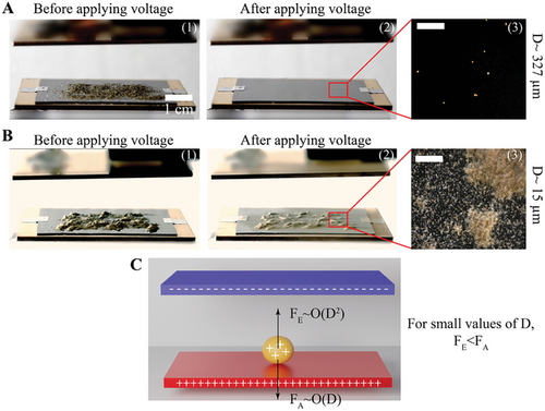
Removing particles with a diameter below ≈ 10 µm is crucial in solar panel application since most dust particle size distributions include values below ≈ 10 µm as characterized in data collected from several solar farms around the world.[27] Thus, for efficient operation of solar power farms, small particles have to be removed completely to eliminate the usage of water for cleaning. Since electrostatic field cannot be increased beyond Emax = 3 MV/m due to breakdown, a practical way to remove smaller particles is by reducing the Van der Waals force of adhesion.
Van der Waals force is universal in nature and acts between all materials within a short-range of less than ≈1 nm.[28-30] There are mainly two means of reducing Van der Waals force: by changing the surface chemistry to reduce the Hamaker constant or by changing the surface morphology to reduce the degree of contact between particle and substrate.[31, 32] Since electrostatic dust removal applications require transparent and conductive surfaces, the material choices for varying Hamaker constant are limited. Moreover, the order of magnitude of Hamaker constant that affects the Van der Waals force of adhesion does not vary significantly across conductive materials (≈ 10−20 J).[28] Therefore, reducing the degree of contact between particle and substrate is one of the most effective ways to reduce Van der Waals force of adhesion.[33]
To reduce the contact area between particle and surface, textures can be applied to the surface. Since the dust accumulation on solar panels is mostly confined in the micro-particle regime, the effect of texture is apparent only when the size of the texture is comparable (micro-texture) or smaller than that of the particle diameter (nano-texture). There are various micro-scale features that can be introduced on surfaces such as micro-pillars, cones, pyramids etc.[34, 35] Nano-textured surfaces offer more dense, smaller scale features that could have significant impact on the force of adhesion.[36, 37]
In this paper we investigate the effect of surface texture on the efficacy of electrostatic dust removal in the micro-particle regime relevant for photovoltaic application. We demonstrate that nano-textured surfaces significantly reduce the force of adhesion of dust/micro-particles compared to micro-scale textures. We perform electrostatic dust removal experiments and show that the reduced adhesion manifests as a significant reduction in dust particle coverage after the application of voltage, i.e., nano-textured surfaces show 10% coverage of dust particles while micro- and non-textured surfaces show a 35% coverage for particles below 30 µm. We quantify the reduction in adhesion force due to texture by performing atomic force microscopy (AFM) pull-off experiments and show that nano-texture reduces the force of adhesion by up to 2 orders of magnitude compared to non-textured surface, thus presenting a compelling case for having nano-textured surfaces for enhancing small particle dust removal. Finally, we fabricate transparent, electrically conductive, nano-textured glass that can be retrofitted on solar panel surfaces using scalable nano-fabrication technique and show that we can recover >90% of lost power output for particles as small as 5 µm.
2 Results and Discussion
2.1 Nano-Textured Surface is Significantly More Effective for Electrostatic Dust Removal
The adhesion of a dust micro-particle onto a substrate is a sub-micron phenomenon. The region of contact between a single particle and substrate is much smaller than the particle diameter itself for all substrates.[25, 29] Prior to investigating a the interactions between a single particle and the substrate, we experimentally study the removal of dust particles as a collection from textured and non-textured surfaces. This is crucial since the loss of power output in solar panels due to dust accumulation is a function of the total dust coverage.
Even though there are various kinds of surface textures that can be fabricated, including groves, cones, posts etc.,[38, 39] we are primarily interested in the effect of the length scale of texture because the force of adhesion is, at the first order, dependent on the RMS surface roughness.[40, 41] We therefore fabricate micro-post array surfaces and nano-textured nano-grass surfaces[42] on silicon wafers. Micro-posts are fabricated using standard photolithography[43] and nano-grass is fabricated using reactive ion etching (RIE).[44] These surfaces enable us to perform highly repeatable dust adhesion experiments. Figure 2A–C shows SEM images of non-textured silicon, micro-textured silicon, and nano-textured silicon respectively before covering the surface with dust.

To study the relation between electrostatic dust removal and force of adhesion, we perform systematic electrostatic dust removal experiments as in Figure 1. The silicon wafer is placed on the bottom electrode, a 3 mm thick copper plate that is connected to the high-voltage power supply, and ≈3 cm beneath the top electrode, a 5 mm thick, grounded aluminum plate covering the entire bottom electrode. The applied voltage is 15 kV. At the start of the experiments, the substrate is fully covered with dust particles before applying voltage. Followed by application of voltage for 10s, we image the residual dust particles using microscope as shown in sample experimental images (Figure 2D–F). While non-textured and micro-textured surfaces retain a significant portion of small dust particles for particle diameter <100 µm, on nano-textured surface most particles can be removed.
We quantify the dust removal for dust particles of various average diameters as shown in Figure 2G. For large particles >100 µm there is negligible effect of surface texture because Van der Waals force of adhesion is much smaller than electrostatic force of repulsion. However, as the particle diameter decreases (<100 µm), particle removal becomes harder due to domination of adhesion as also evident by the increase in percentage area covered. As the particle diameter decreases below ≈30 µm, a significant portion (≈35%) of the surface area is covered by dust particles for both non-textured and micro-textured surfaces. The micro-textured surface, however, is nominally better, due to slightly reduced degree of contact between dust particles and the surface as particles are positioned on the edges of the micro-posts (Figure S1C, Supporting Information). However, since the length scale of textures are on the same order as the dust micro-particles, most of the dust particles distributed atop micro-posts experience a flat surface when resting on top of micro-posts (Figure S1B, Supporting Information) or in between (Figure S1D, Supporting Information). As a result, on average the total dust coverage when we use micro-textured surface is comparable to that of the non-textured surface. However, when the surface is nano-textured, there is significant improvement in dust removal as shown in Figure 2F. The nano-texture reduces the contact area (Figure S1E, Supporting Information), resulting in much lower Van der Waals force of adhesion and significantly better electrostatic dust removal.[36, 40, 45]
2.2 Quantifying the Force of Adhesion Using AFM Pull-Off Experiments
Macro-scale dust retention on the substrate after application of voltage is affected by the adhesion force due to particle-substrate interactions on a nanoscopic length scale. To probe this interaction further, we study the adhesion of a single micro-particle on non-textured, micro-textured, and nano-textured surfaces. For this, we use Atomic Force Microscope to quantify the parameter called “pull-off” force which is the critical force required to remove a particle from the substrate.[36, 46]
The pull-off force measurements are performed using a multi-mode atomic force microscope (AFM) operated on a Oxford Instruments Asylum Research MFP-3D. Colloidal probes are used in the force spectroscopy measurements.[47] Dust particles are modeled by attaching a spherical silica (SiO2) bead of diameter 5 µm to the cantilever tip, as shown in Figure 3A. Cantilevers with spring constants ranging from 0.01 to 10 nN nm−1 are used for pull-off force measurements. The spring constant is chosen specifically for each experiment to maximize force sensitivity, while constraining the cantilever deflection within the linear range (see Experimental Section). Prior to the experiments, the spring constants of the cantilevers are determined based on the ambient thermal fluctuations. We also eliminate the effect of the static charge by electrically grounding the substrate and the experimental setup.
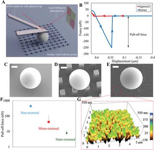
Figure 3B shows a typical pull-off force experiment where we plot the force measured using AFM cantilever as a function of z-axis movement. During the approach of the cantilever to the surface of the substrate (red line) the force is initially close to zero. Then the probe contacts the substrate as shown by a sudden increase in the red curve. To measure pull-off force, the cantilever is retracted away from the substrate. As the particle attached at the tip of the cantilever remains on the substrate due to Van der Waals force of adhesion, the cantilever bends which appears as a sloped negative force measurement as shown in the blue curve of Figure 3B. Pulling the cantilever further away from the substrate causes the particle to suddenly lose contact with the surface resulting in a sudden jump in the force-displacement curve as shown in Figure 3B. This is the pull-off force.
We perform several AFM pull-off experiments on non-textured, micro-textured, and nano-textured surfaces using a silica bead with a diameter of 5 µm attached to the cantilever tip. Figure 3C–E show SEM images of a 25 µm silica bead on different surfaces, to illustrate the scale of the particle and scale of surface texture. While the scale of the micro-texture is comparable to particle diameter, nano-texture is significantly smaller (Figure 3E).
In Figure 3F the average pull-off force to remove the cantilever bead from the three substrates is plotted. As shown in the plot, the non-textured surface has the highest Van der Waals force due to the highest degree of particle-surface contact. The force measurement was consistent between experiments. Pull-off force experiments on micro-textured surfaces have high variability depending on the location where the cantilever bead taps on the surface. Each datapoint in Figure 3F is an average of 192 pull-off force measurements obtained by tapping different points on the substrate from a square grid of 8 × 8 points spaced apart by 2 µm at 3 different locations on the substrate. Thus, depending on the relative orientation of the 8 × 8 tapping grid and the micro-post array, the pull-off force measurement varies significantly between experiments as shown by the error bar. When the cantilever bead taps exactly on top of the post, the pull-off force measurement is the highest and is comparable to that of non-textured surface force measurements (see Figure S2A,B, Supporting Information). When the cantilever bead is simultaneously contacting the corners of micro-posts as shown in Figure S2D (Supporting Information) the pull-off force is the lowest as shown in Figure S2C (Supporting Information). On an average, the pull of force of the micro-textured surface is still significantly higher than that of the nano-textured substrate.
In dust removal experiments where the particle diameter has a non-monodisperse distribution, there will be particles with diameter less than or almost equal to or larger than the post-spacing. The advantage of having micro-post texture for reducing adhesion is only realized for those particles in the distribution that end up being deposited between the edges or between the corners of micro-posts. In other cases, the particles rest exactly on top of one or multiple micro-posts or at the bottom between the posts. Moreover, there could be particles that are stuck between posts and are more difficult to remove compared to removing dust particles from a non-textured surface. Therefore, removal of dust particles from micro-textured surface to reduce the total surface coverage after application of voltage is challenging as demonstrated in Figure 2E.
Finally, the pull-off force measurement experiments on the nano-textured surface show that the average force of adhesion is about two orders of magnitude lower compared to the non-textured surface. This is a consequence of the significantly smaller length scale of the nano-texture compared to the particle diameter. Figure 3G shows the topology of the nano-textured surface generated by AFM scan using a tipless cantilever. The average feature size (height and width) is ≈200 nm.
2.3 Fabrication of Transparent, Electrically Conductive, Nano-Textured Glass
As demonstrated in Figure 3, nano-texture significantly enhances electrostatic dust removal. However, for applying this concept to solar panels, we require the following characteristics for the solar panel surface: 1) high transparency, 2) sufficient electrical conductivity for inducing charge on dust particles, and 3) nano-texture for reducing Van der Waals force of adhesion. Thus, for enabling practical application enhanced electrostatic dust removal from solar panels, our goal is to fabricate a novel surface that is transparent, electrically conductive, and nano-textured.
Fabrication of a glass surface with the above characteristics can be divided into a two-step process of 1) texturing the glass and 2) coating the texture with any TCO (Transparent Conductive Oxide) material such as Indium doped Tin Oxide (ITO) or Aluminum doped Zinc Oxide (AZO). There are several potential techniques to fabricate textured glass including chemical etching,[48] nano-wire growth via sol-gel process,[49, 50] laser etching[51] etc., resulting in different kinds of textures. Scalability of the etching process for different sample sizes is a major consideration for practical application. We use copper nano-drop-mask based reactive ion etching process to create nano-textured glass[52] which is agnostic to the substrate sample size and therefore can be potentially translated to solar-panel scale glass samples.
We fabricate nano-textured glass in a multi-step process proposed by Infante et al.[52] In the first step as shown in Figure 4A(1) we sputter deposit a 5 nm thick copper layer on the fused silica glass substrate of softening point 1700 °C, thickness 2 mm, and a sample size of 2.5 cm x 2.5 cm. In the second step we heat the substrate to 750 °C (Rapid Thermal Annealing) which is below the melting point of copper (1085 °C) that results in the de-wetting of the copper layer from the glass surface to form nano-scale copper droplets as shown in Figure 4A (2). After the substrate cools down, the copper droplets solidify, to form nano-scale mask on the glass surface as shown in the SEM image of Figure 4B. Then we etch the substrate using Reactive Ion Etching (RIE) (Figure 4A (3)) which results in nano-scale features with copper deposition atop the features. This happens because copper does not get etched and acts as a mask, whereas the remaining portion of the glass is exposed to RIE process. Then we wash away the copper using acid washing (Figure 4A (4)) resulting in nano-texture on the glass as shown in the SEM image of Figure 4C. By the end of this step, we obtain a transparent nano-textured glass with average feature size ≈200 nm (Figure 4C–F).
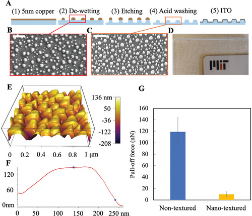
In the last fabrication step (Figure 4A (5)) we conformally coat the surface with 15 nm thick ITO to make the surface conductive while maintaining transparency and surface features (see Experimental Section for more fabrication details). Figure 4D shows the image of the glass surface for qualitative demonstration of transparency. The relative transmittance of nano-textured glass is as high as non-textured glass as shown in Figure S4 (Supporting Information). For performing control experiments, we also fabricated non-textured glass surfaces with 15 nm thick ITO coating. Figure 4E,F show the AFM surface morphology of nano-textured glass. The scale of the morphology is comparable to that of silicon nano-grass surface with a feature size of ≈200 nm. In Figure 4G we plot the AFM pull-off force of 5 µm silica beads from nano-textured and non-textured glass surfaces. There is a significant reduction in force of adhesion similar to the case of silicon substrate. The pull-off forces are measured for and non-textured and nano-textured samples and are found to be ≈120 and ≈10 nN respectively (Figure 4G). The pull-off force measurement shows that, similar to nano-textured silicon, we are able to successfully fabricate nano-textured, transparent conductive glass substrates that significantly reduces the force of adhesion.
2.4 Power Output Recovery from Bench-Top Electrostatic Dust Removal System
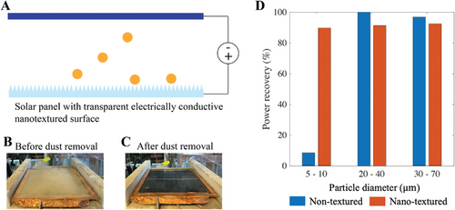
We perform electrostatic dust repulsion experiments using different dust particle diameters and quantify the power output before and after dust removal. The control experiments are performed using ITO-coated non-textured glass surfaces. A high-voltage supply is connected to the glass electrode and another parallel plate metallic electrode is used as the electrical ground with a gap of 1 cm between both electrodes and ≈12 kV are applied for 10s as shown in Figure 5A (see Experimental Section).[11]
Figure 5B,C shows the surface of the solar panel with a conductive nano-textured glass panel installed before and after dust removal. Voltage is applied for 10s to the electrode using copper tapes for ensuring proper electrical contact between the power supply and the textured glass (see methods). We perform dust repulsion experiments using particle diameters ranging from 5 to 70 µm and quantify the power output recovery.
The power output is quantified by measuring the voltage across a resistor of 1000 ohm resistance connected between the solar panel leads (see Experimental Section). Figure 5D shows the power output recovery for different particle diameters using non-textured and nano-textured surfaces. For particles above or equal to 20–40 µm, both non-textured and nano-textured surfaces perform equally well, recovering 90% of the lost power output since electrostatic force of repulsion overcomes the Van der Waals force of adhesion. However, as particle diameter gets below 10 µm and adhesion dominates, we observe that for non-textured surface only ≈8% of the lost power output can be recovered whereas nano-textured surfaces enable power output recovery of 90%.
The power consumption of this device is estimated by limiting the current of the power supply to 0.01 mA for cleaning a 100 cm2 solar panel. For an applied voltage of ≈12 kV this results in a maximal power consumption of 12 W m−2, which is negligible considering the 500 W m−2 power output of the solar panel. Hence, the power required for the cleaning system can be fully supplied by the solar panel. We envision, this system to be run sporadically when cleaning is necessary. Hence, the total energy consumption is also negligible.
Our approach demonstrates that by utilizing surfaces with texture length scales which are one order of magnitude smaller than that of the diameter of target dust particles, we can significantly enhance the capabilities of charge induction based electrostatic dust removal systems. By enabling removal of most of the dust particles above 5 µm, our electrostatic dust removal approach has the potential to enable the operation of more than ≈75% of the solar farms with zero water footprint.[27]
3 Conclusion
In this paper we demonstrate that electrostatic dust removal for solar panel cleaning for particle diameters smaller than 10 µm can be significantly enhanced using nano-textured surfaces. Using AFM pull-off experiments we demonstrate that nano-textured surfaces can have up to two orders of magnitude reduction in Van der Waals force of adhesion compared to non-textured or micro-textured surfaces. We show that the reduction in pull-off force manifests as a ~3.5-fold enhancement of electrostatic removal of <30 µm particles compared to non-textured or micro-textured surfaces, i.e., nano-textured surfaces have a 10% coverage while textured surfaces have a 35% coverage. To translate this finding into application on solar panels that require transparent surfaces, we fabricate transparent, electrically conductive, nano-textured glass that can be retrofit to solar panels. We fabricate the textured glass substrates using a scalable copper nano-mask such that the approach can be also translated to full-scale solar panel glass -surfaces. We design a bench-top solar panel dust removal setup with nano-textured solar panel and show that we can recover 90% of lost power output for particles ≥20–40 µm and recover 90% of lost power output for particles smaller than 10 µm, making this technology highly applicable for solar farms. Further, we estimate the power consumption of the dust repulsion mechanism to be lower than 12 W m−2, which is negligible compared to 500 W m−2 power output of a typical solar panel. Given the tremendous potential and global applicability of active dust repulsion system in photovoltaics, our approach that enables significantly higher dust removal efficiency for particle diameters smaller than 10 µm has the potential to eliminate the water footprint of photovoltaic systems, contributing to truly sustainable operation of solar farms.
4 Experimental Section
Dust Particles
Arizona road dust from Powder Technology Inc. with fractions of 5–10 µm, 10–20 µm, 20–40 µm, 30–70 µm, 53–106 µm, 106–212 µm, 212–300 µm, and 300–355 µm was used. To simplify Figure 2, the data is plotted as function of the average particle size of these fractions, which is approximated with the mean value of the upper and lower bound.
AFM Pull-Off Force Experiments
The pull-off force measurements were performed using a multi-mode atomic force microscope operated on a Oxford Instruments Asylum Research MFP-30. Since dust particles consist of ≈75% silica (SiO2)[53, 54] a cantilever tip with a silica bead of diameter 5 µm attached to it, was used. The cantilever with the attached bead was purchased from Novascan. Cantilevers with spring constants ranging from 0.01 to 10 nN nm−1 are used for pull-off force measurements. For non-textured surfaces, since force of adhesion was highest, the AFM measurement either becomes non-linear or saturate for low spring constants. Therefore, stiffer cantilever (≈10 nN nm−1) was selected for non-textured surfaces and compliant one (≈0.01 nN nm−1) for nano-textured surfaces. The spring constants of the cantilevers were calibrated based on the ambient thermal fluctuations. Static charge build-up was prevented by electrically grounding the substrate and the experimental setup to not have its effect in force of adhesion. Finally, temperature was kept at 20 °C and ambient humidity was between 30 and 40%, thus making capillary effects negligible.[25]
Creating Nano-Texture on Glass Surface
Samples of two different sizes were fabricated using fused silica samples. For characterization purposes 2.5 cm x 2.5 cm x 0.1 cm samples, and for the power recovery experiments 10 cm x 10 cm x 0.16 cm samples were fabricated. The fabrication of nano-textured glass contained four steps:[52] 1) deposition of 5nm copper film on fused silica via sputtering, 2) rapid thermal annealing (RTA), 3) reactive ion etching (RIE), and 4) cleaning sample with acid (a mixture 75 wt.% phosphoric acid, 5 wt.% nitric acid, and 20 wt.% DI water). The AJA Orion 5 sputter system was used to deposit copper at a rate of 0.05 nm s−1 in a pure Argon atmosphere. RTA was carried out at 750 °C for 100 s in 1 atm N2 atmosphere using the AnnealSys AS One-150. To etch the samples, the SAMCO 230iP was used. The samples were etched for 90 s at 1 Pa, 400 W using 30 sccm CF4 and 60sccm Argon plasma.
ITO Deposition on Glass
The AJA Orion 5 sputter system was used to deposit 15 nm thick indium tin oxide at a rate of 0.05 nm s−1 in a pure Argon atmosphere. After deposition of ITO, 2–5mm wide area around the edges was sputtered with a 100 nm thick layer of copper, enhancing the electrical contact between sample and the conductive tape, which was used as the electrical connection to the power supply (see Figure S3, Supporting Information; Figure 5B,C).
Transmittance Measurement
The transmittance was measured with a PerkinElmer LAMBA 1050 UV/Vis/NIR Spectrometer for three different 2.5cm × 2.5cm × 0.1cm fused silica samples: 1) uncoated and non-textured 2) coated with 15 nm ITO and non-textured and 3) coated with 15 nm ITO and nano-textured. The ITO coating on the non-textured sample reduces the transmittance compared to the uncoated and non-textured sample (Figure S4, Supporting Information). However, the nano-texture reduced reflective losses and therefore increased the total transmittance[52] compared to the samples (1) and (2) (Figure S4, Supporting Information).
Conductivity Measurement
The conductivity (Table 1) was measured with a four-point probe on two 2.5cm × 2.5cm × 0.1cm fused silica samples: 1) coated with 15 nm ITO and non-textured and 2) coated with 15 nm ITO and nano-textured. The conductivity was measured with a 4-point-probe[55] from Ossila at five different locations each, repeating conductivity measurements 25 times at each location. Finally, the average for each sample was calculated by averaging over all conductivity values. The probe spacing of the 4-point-probe was 5 mm. Although the film thickness was identical for both samples, the conductivity for the nano-textured sample was significantly lower and had a high variation, due to a larger pathlength for the current resulting from the texture and the reduced contact area between the probes and the nano-textured surface. The conductivities for both, the nano-textured and non-textured ITO-coated substrates (Table 1) were significantly higher than the conductivity of the dust layer, which was estimated to be on the order of 10−7 S m−1.[22] Hence, the charging of the dust particles was not limited by the ITO coating, but only by the conductivity of the particles.
| Surface type | Conductivity (S m−1) |
| Non-textured ITO coated | 335.7 ± 62.3 |
| Nano-textured ITO coated | 7.13 ± 5.6 |
Power Output Measurements
Power output recovery from solar panels was performed on a 1 W solar panel purchased from Fielect. The study used a Phlox white light to simulate sunlight inside the lab. The study performed dust repulsion experiments and power output measurements separately. First, the nano-textured glass panel was installed on the solar panel with a parallel plate metallic electrode on top with a distance of 1 cm. The top electrode consisted of a 5mm thick, grounded aluminum plate. Dust particles of sizes from 5 to 70 µm (in separate experiments) were uniformly distributed on the glass panel surface to reduce the power output by 20–25% compared to the power output in the absence of dust, which was a common soiling loss.[4] Then the study applied ≈12 kV between the glass panel and the top electrode for 10s. This electric field was above the critical strength for all particle diameters and still prevented arcing at the sharp edges of the electrodes.[11] After repelling the dust, the voltage was switched off and the solar panel was placed at a precise location below the light source. The study connected the solar panel power output leads to a resistor of resistance 1000 ohm and measured the voltage across the resistor. Using the measured voltage and resistance values, the power output from the solar panel was obtained.
Acknowledgements
The authors thank Alan F. Schwartzman (MIT NanoMechanical Technology Lab) for helping with the AFM experiments and for fruitful discussions related to this work. The authors also thank Bert Vandereydt for fruitful discussions and James M Daley (MIT Nano) for helping with SEM imaging. This work was supported by Eni S.p.A. through the MIT Energy Initiative.
Conflict of Interest
The authors declare no conflict of interest.
Author Contributions
F.J.D. and S.P. contributed equally to this work. S.P, F.J.D, and K.K.V. conceived the project. S.P, F.J.D, and K.K.V. analyzed the data and wrote the paper. S.P and F.J.D carried out the experiments. K.K.V. supervised the work.
Open Research
Data Availability Statement
The data that support the findings of this study are available from the corresponding author upon reasonable request.


