Electrical Polarity Modulation in V-Doped Monolayer WS2 for Homogeneous CMOS Inverters
Abstract
As demand for higher integration density and smaller devices grows, silicon-based complementary metal-oxide-semiconductor (CMOS) devices will soon reach their ultimate limits. 2D transition metal dichalcogenides (TMDs) semiconductors, known for excellent electrical performance and stable atomic structure, are seen as promising materials for future integrated circuits. However, controlled and reliable doping of 2D TMDs, a key step for creating homogeneous CMOS logic components, remains a challenge. In this study, a continuous electrical polarity modulation of monolayer WS2 from intrinsic n-type to ambipolar, then to p-type, and ultimately to a quasi-metallic state is achieved simply by introducing controllable amounts of vanadium (V) atoms into the WS2 lattice as p-type dopants during chemical vapor deposition (CVD). The achievement of purely p-type field-effect transistors (FETs) is particularly noteworthy based on the 4.7 at% V-doped monolayer WS2, demonstrating a remarkable on/off current ratio of 105. Expanding on this triumph, the first initial prototype of ultrathin homogeneous CMOS inverters based on monolayer WS2 is being constructed. These outcomes validate the feasibility of constructing homogeneous CMOS devices through the atomic doping process of 2D materials, marking a significant milestone for the future development of integrated circuits.
1 Introduction
Complementary metal-oxide-semiconductor (CMOS) devices, underpinned by the efficient integration of p- and n-type channels, form the cornerstone of modern logic circuits. As the quest for reduced power consumption and device miniaturization continues, traditional silicon-based technologies are rapidly approaching their inherent limits because of the notorious short-channel effect.[1, 2] This reality has triggered an urgent search for innovative materials and integration technologies. Consequently, extensive research is being conducted on ultrathin, 2D semiconductors as a potential solution to overcome these size scaling limits.[3-8] Amongst various 2D materials, transition metal dichalcogenides (TMDs) are emerging as the most promising candidates due to their remarkable electrical properties and atomic-level stability.[9-15]
In recent years, considerable efforts have been directed toward constructing heterogeneous CMOS electronics utilizing TMDs, with two different materials of distinct electrical polarities serving as n-channel and p-channel, respectively.[16-19] However, it is important to highlight that the large-scale integration of such heterogeneous CMOS electronics, which depend on two different channel materials, presents significant challenges and is often impractical. Therefore, developing reliable homogeneous CMOS devices using TMDs is a critical step forward for practical applications.[20] Consequently, the ability to reliably modulate the electrical polarity in TMDs is not just desirable but absolutely essential.
Doping offers an efficient method that involves the manipulation of the intrinsic physicochemical properties of semiconducting TMDs, thereby enhancing the functionalities of devices built on intricate nanostructures. Generally, doping in TMDs typically falls into two categories: surface charge transfer doping[21-23] and substitutional doping.[24-26] Surface charge transfer dopants, prone to surface desorption, are less suitable for long-term robust doping. In contrast, substitutional doping involves incorporating dopants into the lattice structure, forming strong chemical bonds that enhance stability and reliability, making it more favorable for device applications.[25, 27] By introducing metal dopant atoms like V,[26, 28-32] Nb,[33-36] Re,[26] Fe,[37] and In[38] into the TMD lattice to substitute transition metal atomic, effective modulation over the intrinsic electrical polarity and carrier types of TMD materials have been achieved. However, the simultaneous realization of high-performance, stable, purely n-type field-effect transistors (FETs) and p-type FETs based on the same material through atomic substitution doping processes, a clear requirement for homogeneous CMOS manufacturing techniques at the circuit level, has thus far failed. Furthermore, constructing stable CMOS devices in TMDs through substitutional doping processes is still an unrealized goal.
Given these challenges, we choose WS2 as a dopant acceptor for its excellent chemical stability and stable purely n-type semiconductor characteristics,[39] aiming to develop a controllable technique to reliably modulate the electrical polarity in monolayer WS2. This would enable the fabrication of high-performance homogeneous CMOS logic components. Specifically, we leveraged the liquid-phase reaction precursors and the chemical vapor deposition (CVD) method to introduce vanadium (V) atoms into the WS2 lattice as p-type dopants via atomic substitution. The flexibility of our preparation process allowed us to successfully control the doping ratio of V atoms within the WS2 lattice by simply adjusting the precursor solution ratio. As the doping ratio increased, we achieved continuous modulation of the electrical polarity of monolayer WS2, transitioning from intrinsic n-type to ambipolar, then to p-type, and ultimately to a quasi-metallic state. Notably, we achieved purely p-type FETs with the 4.7 at% V-doped monolayer WS2 channel, delivering an impressive on/off current ratio of 105. Capitalizing on this success, we combined them with intrinsic n-type WS2 FETs, effectively constructing the first prototype of homogeneous WS2 CMOS inverter devices. This achievement represents a significant advancement in the future development of integrated circuits.
2 Results and Discussion
The fabrication of V-doped monolayer WS2 via the CVD method is depicted in Figure 1a. A well-mixed precursor solution containing W atoms ((NH4)6H2W12O40•xH2O, AMT) and V atoms (NH4VO3, AMV) in specified proportions was prepared and spin-coated onto a SiO2(270 nm)/Si substrate to generate a uniformly thick precursor film (Figure S1a, Supporting Information). During the spin-coating process, it was observed that the crucial step of pretreating the SiO2/Si substrate with oxygen plasma enhances hydrophilicity by introducing oxygen-containing groups on the substrate surface,[40] facilitating the even distribution of the precursor solution. In contrast, substrates without oxygen plasma treatment showed ineffective spin-coating of the precursor solution (Figure S1b,c, Supporting Information). Subsequently, an as-cleaned SiO2/Si substrate was placed face-to-face on top of the substrate coated with the reaction precursor, creating a confined space conducive to the growth of monolayer WS2 (Figure S2, Supporting Information). Under sulfur-rich conditions, the construction of this confined space provides stable sulfur vapor and a broader growth window.[41] The optimal growth results were observed on the upper SiO2 substrate surface, as depicted in the Optical Microscope (OM) image in Figure 1b. Typical equilateral triangle-shaped and uniformly textured WS2 single-crystal domains were observed. Atomic Force Microscopy (AFM) was utilized to analyze the height profile and to confirm a thickness of ≈0.9 nm, indicating the monolayer structure here.[42] Energy-Dispersive X-Ray Spectroscopy (EDS) was next employed to characterize the element distribution within the domains, confirming the successful preparation of WS2 and the effective doping of V atoms (Figure S3, Supporting Information).
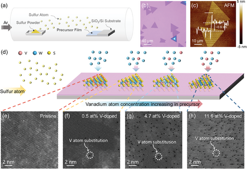
Compared to the solid-state sources, the solution-based precursor preparation method offers significant flexibility. By simply adjusting the ratio of W and V atoms in the solution, effective control over the V doping ratio in the WS2 lattice can be achieved (Figure 1d). Using this method, we successfully prepared single-crystal WS2 domains with varying V doping ratios, as shown in the OM images in Figure S4a–d (Supporting Information). Their domain sizes and color contrasts did not exhibit significant differences. The corresponding high-angle annular dark-field scanning transmission electron microscope (HAADF-STEM) images of V-doped monolayer WS2 with different doping ratios were presented in Figure 1e–h. In these images, distinct and visually apparent sites where V atoms replaced W atoms in the WS2 atomic structure were observed (darker contrast is observed at V substitution sites due to the smaller atomic number than W). The distribution of V substitution sites within the WS2 lattice was uniform, without noticeable clustering. Based on a statistical analysis of the number of V atoms and transition metal atomic sites (Table S1, Supporting Information) shown in the HAADF-STEM images, four different single-crystal WS2 domains were prepared in this experiment, corresponding to doping ratios of 0% (pristine), 0.5%, 4.7%, and 11.6%, respectively.
Raman spectra of the pristine and V-doped monolayer WS2 were obtained using a laser with a wavelength of 532 nm (Figure 2a). Both pristine and V-doped samples exhibit characteristic E2g and A1g peaks of 2D WS2,[43, 44] corresponding to in-plane vibrations of W and S atoms (Figure 2b) and out-of-plane vibrations of S atoms (Figure 2c), respectively.[45] Compared to the pristine WS2, a series of systematic changes are observed in the Raman spectra with the increasing V doping ratio. It is noted that the intensity of the E2g peak significantly decreases with higher doping ratios, attributed to increased lattice disorder resulting from the substitution of W atoms by V atoms within WS2.[28, 31, 46] Conversely, the intensity of the A1g peak, influenced solely by the vibration mode of S atoms, shows no apparent change. Also, the ratio of E2g to A1g peak intensities differs notably among pristine and various doping ratios of WS2 (Figure S5, Supporting Information). Raman mapping images of the E2g and A1g peak intensities for the pristine and V-doped monolayer WS2 with different doping ratios under 532 nm laser excitation in the regions corresponding to the optical images are shown in Figure S6a–d (Supporting Information). The corresponding ratio of E2g to A1g peak intensities images are presented in Figure 2d–g. Importantly, this feature demonstrates good consistency within the entire crystal domain, further emphasizing the uniformity of V doping within the lattice. Remarkably, the position of the E2g peak exhibits a strong correlation with the doping, showing a blue shift attributed to the changes in the internal electronic structure of WS2 induced by doping (Figure S7a, Supporting Information). This phenomenon is commonly observed in various p-type doped TMD materials, where corresponding n-type doping leads to a red shift of the characteristic peak.[46] Furthermore, with the increase in the doping ratio, three additional peaks at 146.6 cm−1 (J1), 215.2 cm−1 (J2), and 385.4 cm−1 (J3) emerge (Figure S7a,b, Supporting Information). These peaks are characteristics of the metallic phase (1T). They are absent in the semiconducting phase (2H) of 2D WS2,[47, 48] indicating that V doping induces a phase transition from 2H to 1T in WS2.
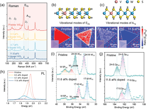
The photoluminescence (PL) spectra of the pristine and V-doped monolayer WS2 show a consistent dependence on the dopant ratio (Figure 2h). The corresponding spatially resolved PL intensity mapping images are shown in Figure S8a–d (Supporting Information). The pristine WS2 monolayer exhibits a robust PL peak at 1.96 eV, while the V-doped WS2 undergoes a redshift of 30 meV (0.6 at% V-doped WS2) and 100 meV (4.7 at% V-doped WS2). Concurrently, the PL peaks broaden and experience a reduction in the intensity, probably arising from lattice disorder induced by dopants coupled with an increased density of positive trions[30, 32, 49] since vanadium is anticipated to act as a p-type dopant in WS2.[50] As the dopant ratio reaches 11.4 at%, the PL signal has almost complete quenching. This observed PL quenching is postulated to be attributed to the metallic nature induced by doping, aligning with the Raman results discussed above.
To demonstrate the phase transition from 2H to 1T induced by V doping in WS2, XPS was employed to characterize the as-synthesized pristine and V-doped monolayer WS2. The tungsten signal exhibits sensitivity to its oxidation state and coordination geometry. Consequently, by monitoring the position of the binding energy in the W 4f7/2 and W 4f5/2 core level peaks, an unambiguous distinction between the 1T and 2H structures can be made.[47, 51] The XPS spectra of W 4f core level characterization results of the pristine and V-doped monolayer WS2 shown in Figure S9 (Supporting Information) illustrate that the introduction of V atoms brings about 1T phase components within the WS2 lattice, and the proportion of 1T phase increases with the doping ratio. As depicted in Figure 2i, the W 4f core level peaks exhibit an ≈0.9 eV shift to lower binding energy in the 4f7/2 (31.6 eV) and 4f5/2 (33.8 eV) peaks of the 11.6 at% V-doped WS2 compared to 4f7/2 (32.5 eV) and 4f5/2 (34.7 eV) peaks of the pristine WS2. This shift indicates the lower valence state of W elements in the 11.6 at% V-doped WS2 crystals, consistent with previous XPS studies on the 1T metallic WS2.[48] The observed oxidation (W6+ at 36.2 eV) can account for the morphological damage caused by X-ray irradiation during characterization. At the same time, the high-resolution core level S 2p peaks of the 11.6 at% V-doped WS2 consistently exhibit a lower binding energy of ≈1.0 eV compared to the S 2p peaks from the pristine WS2 (Figure 2j). Combining the existing Raman and PL characterization results, we posit that introducing V atoms into WS2 affects the lattice order. The increasing doping ratio induces a structural transition in WS2 from the 2H (semiconductor state) to the 1T phase (metallic state). Analyzing the W 4f spectra, it is estimated that the proportion of the 1T phase in the 11.6 at% V-doped WS2 in our experiment is ≈90%. In addition, XPS spectra of V 2p for the pristine and V-doped monolayer WS2 are shown in Figure S10 (Supporting Information). The vanadium doping levels of 0.5 and 4.7 at% were below the XPS detection limit. In comparison, the 11.4 at% V-doped monolayer WS2 exhibited a distinctive doublet signal, indicative of binding energies at 524.5 eV for V 2p1/2 orbital electrons and 517.0 eV for V 2p3/2 orbital electrons.
To further validate the structural changes induced by V doping in WS2, we characterized the pristine and V-doped monolayer WS2 microstructures. The HAADF-STEM image of the as-prepared pristine WS2 showcases a hexagonal packing along the [001] zone axis, a characteristic feature commonly observed in monolayer WS2 (Figure 3a). This arrangement is further confirmed by the selected area electron diffraction (SAED) pattern (inset in Figure 3a). The zoom-in view in Figure 3b allows for the direct observation of the alternating arrangement of W and S atoms in a hexagonal ring structure, confirming that the experimentally prepared pristine WS2 possesses semiconductor properties with a 2H phase. Also, its structural model from side and top views is depicted in Figure 3d. Furthermore, the intensity profiles in Figure 3c (bottom, from the red dashed box in the top image) indicate an adjacent W–W atomic distance of 3.18 Å. Similarly, high-resolution HAADF-STEM images of the 0.5 and 4.7 at% V-doped WS2, as well as the pristine WS2, display the 2H phase structure (Figure S11, Supporting Information, with darker contrast at the W atom sites indicating substitutional V atoms), and the W–W atomic distances correspond to 3.17 Å.
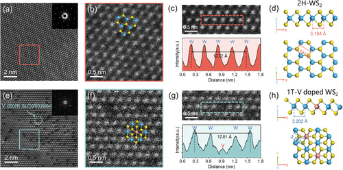
In contrast to the 2H phase, the HAADF-STEM images of 11.6 at% V-doped WS2 reveal a distinctive metallic 1T phase structure (Figure 3e,f). In the top view image, the monolayer WS2 has a typical three-atomic layer (S-W-S) structure. Unlike the A-B-A stacking in 2H-WS2, the 1T-WS2 presents an A-B-C stacking, where the top-layer S atoms do not overlap with the bottom-layer S atoms.[52, 53] The structural difference, coupled with the lower atomic number of S atoms, makes the observation of S atoms in the HAADF-STEM mode more challenging in the 1T phase compared to the 2H phase of WS2. The SAED pattern also demonstrates the pure hexagonal symmetry of the 1T V-doped WS2, indicating the absence of the 1T’ phase component.[54] Intensity profiles reveal a W–W atomic spacing of 3.20 Å in the 1T V-doped WS2 structure (Figure 3g), with the corresponding structural model from the side and top views shown in Figure 3h.
Microstructure always plays a pivotal role in determining materials’ intrinsic properties. To explore the influence of V doping on the electronic characteristics of WS2, FETs were constructed using individual triangular monolayers as the channel material, and their transfer and output characteristics were investigated. Electrostatic gating was achieved through a SiO2 (50 nm)/Si (P++) substrate serving as the back gate electrode. The source/drain contact electrodes, crafted from 50 nm Au, were patterned with a channel length of 4 µm (Figure S12, Supporting Information). Figure 4a–d illustrates the transfer characteristics compiled with the logarithmic y-axis of the pristine and V-doped WS2 with varying doping ratios. The transfer curves in the linear y-axis are shown in Figure S13a–d (Supporting Information). For the pristine WS2 FET device, the insulating behavior is evident at a substantial negative gate bias (VBG = −15 V), transitioning to an “on” state at VBG = 15 V (Figure 4a). This confirms its robust n-type characteristics. With the introduction of V dopants into the WS2 lattice, the threshold voltage of the electron branch shifts toward the positive gate bias, and a hole branch emerges at large negative gate biases. The lightly V-doped (0.4 at%) WS2 exhibits asymmetric ambipolar characteristics (Figure 4b), with both n- and p-branches evident. This behavior strongly indicates that the V dopants serve as electron acceptors. Increasing the doping ratio enhances the p-branch and diminishes the n-branch within the same VBG measurement window. Notably, at a doping ratio of 4.7 at%, the n-type conduction disappears entirely, suggesting sufficient electron acceptors at this V doping ratio. It demonstrates a distinctly p-type character with an on/off ratio reaching ≈105. When the doping ratio reaches 11.6 at%, an unusual observation is made. The FET device exhibits extremely weak p-type behavior and quasi-metallic transport characteristics, as indicated by the significantly enhanced IDS in the transfer curves shown in Figure 4d. We attribute this phenomenon to the structural transition in the WS2 lattice from the 2H phase (semiconductor state) to the 1T phase (metallic state) due to the introduction of a high ratio of V dopants. This conclusion aligns with the aforementioned Raman, PL, XPS, and the HAADF-STEM characterization results of 11.6 at% V doped WS2.
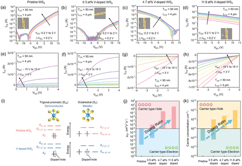
Figure S14a–d (Supporting Information) depicts the IDS–VBG transfer characteristics of the four aforementioned FETs under varying VDS conditions from 0.4 to 2 V in 0.4 V increments, both for the forward and reverse cycles. In the case of the p-type V-doped WS2 (4.7 at%), the maximum voltage difference between the trace and retrace sweeps is <1 V (Figure S14b, Supporting Information), suggesting relatively more stable and controllable characteristics in the charge transfer and switching behavior. Figure S15 (Supporting Information) presents the IDS–VDS output characteristics under different VBG conditions. In the low source-drain bias range, from −0.5 to 0.5 V, the IDS–VDS curves display nearly linear and symmetric behaviors, indicating the formation of effective ohmic-like contacts between the Au contact electrodes and the pristine WS2 (or the V-doped WS2) crystal. When sweeping the source-drain bias up to 4 V (or −4 V), as depicted in Figure 4e–g, all the FET devices, whether n-type (pristine WS2), ambipolar (0.5 at% V doped), or p-type (4.7 at% V doped), exhibit a trend toward saturation in IDS. However, for the monolayer WS2 FET device with the V doping ratio of 11.6 at%, there are no signs of current saturation, even with VDS increased to −4 V. It continues to demonstrate a strictly linear growth trend, with IDS exceeding 10 µA (Figure 4h). This further confirms its quasi-metallic electrical characteristics. Overall, this transition observed in WS2, from intrinsic n-type to ambipolar and then to p-type due to V doping, is compelling evidence of V dopants functioning as electron acceptors, introducing holes as charge carriers for electrical conduction. As the doping ratio gradually increases, structural phase transitions occur within the lattice, leading WS2 to transition from a semiconductor state (2H phase, D3h) to a metallic state (1T phase, Oh).
Structural transitions in monolayer TMDs are intricately tied to the occupancy of electrons in the d orbitals.[53, 55, 56] The H phase adopts a trigonal prismatic structure with hexagonal symmetry (D3h group), causing the d-orbitals of the transition metal to split into three levels. In contrast, the T phase features an octahedral structure with tetragonal symmetry (Oh group), resulting in the formation of two degenerate orbital energies (Figure 4i). Following the crystal field theory, the energy level of the dz2 orbital in the 2H phase is lower than the t2g band of the 1T phase.[55, 56] This suggests that favoring a specific phase can be achieved by appropriately filling the d orbitals with electrons.[57] In the case of the pristine WS2, W belongs to group 6 in the periodic table and possesses 2 electrons in its d-orbitals (Figure S16, Supporting Information). According to the Pauli exclusion principle, these 2 electrons tend to pair in the dz2 orbital of the 2H phase instead of occupying two of the three t2g orbitals in the 1T phase for thermodynamic considerations. Consequently, the 2H phase emerges as the ground state, exhibiting semiconducting properties. However, when W sites are substituted with V atoms from group 5, an additional hole is introduced, occupying the dz2 orbital in the 2H phase. The presence of individual electrons significantly diminishes the energy barrier, resulting in a notable reduction in the energy difference between the 2H and 1T structures as the hole count increases due to p-type charge doping. Consequently, charge doping is a viable approach for inducing the phase transition from the 2H to the 1T structure, thereby showcasing metallic properties.
To further evaluate the performance of the pristine and V-doped monolayer WS2 FETs, the carrier mobility (µ) (Figure S17, Supporting Information; Figure 4j) and carrier concentration (n) (Figure 4k) of the four types of FETs (pristine, 0.4 at%, 4.7 at%, and 11.6 at% V doped monolayer WS2) were extracted from the transfer curves under the bias of VDS = 400 mV in Figure 4a–d. The relatively low carrier mobility (n-type pristine WS2: 0.11 cm2V−1s−1 and p-type V doped WS2: 0.24 cm2V−1s−1) may be limited by the scattering of longitudinal acoustic (LA) phonons[58] and high-density impurity scattering.[59] However, more notably, as the V doping ratio increases, the electron deficiency in the valence band and the emergence of delocalized holes induce the p-doping behavior. This transition from n-type to p-type electrical behavior provides direct evidence that V dopants are electron acceptors, effectively compensating for the natural n-type dopants in the pristine WS2. When the doping ratio reaches 4.7 at%, holes have already dominated the charge transport process, indicating the presence of sufficient electron acceptors and resulting in a fully p-type WS2 semiconductor.
By constructing FET devices to assess the electrical properties of both pristine and V-doped WS2, we observed that the introduction of V atoms as dopants enables continuous and controllable modulation of the electrical polarity of WS2, transitioning from n-type to ambipolar, then to p-type, and ultimately to a quasi-metallic state. Table 1 summarizes recent studies on electrical polarity modulation in TMDs achieved through substitutional atomic doping. The table provides a statistical comparison of the reported capabilities for electrical polarity modulation and the corresponding on/off ratios of the fabricated n-FETs and p-FETs devices. In essence, our research successfully demonstrated effective modulation of the electrical polarity in monolayer WS2 films, and the WS2 FETs with a doping ratio of 4.7 at% exhibited outstanding and competitive p-type performance compared to other reported results. Notably, both the n-type pristine and p-type V-doped WS2 samples prepared as described in our research demonstrated prolonged stability in performance under ambient air conditions (Figures S18 and S19, Supporting Information) and continuous operating voltage (Figures S20 and S21, Supporting Information). These results open up the possibilities for the construction of ultrathin homogeneous CMOS inverters, the most basic logic component, based on monolayer WS2.
| TMDs Doping Acceptor | Dopants | Electrical Polarity Modulation (Yes or No) | On/Off Ratio | Refs. | ||||
|---|---|---|---|---|---|---|---|---|
| n-type | ambipolar | p-type | metallic | n-type | p-type | |||
| WS2 | Niobium (Nb) | Pristine | Y | N | N | 106 | / | [33] |
| Pristine | Y | Y | N | 104 | 105 | [36] | ||
| Pristine | Y | Y | Y | 107 | 104 | [35] | ||
| WSe2 | Rhenium (Re) | N | Pristine | N | Y | / | / | [25] |
| WS2 | Sodium (Na) | Pristine | N | Y | N | 105 | 104 | [60] |
| MoSe2 | Tungsten (W) | Y | Y | Pristine | N | 105 | 105 | [61] |
| WS2 | Vanadium (V) | Pristine | Y | N | N | 107 | / | [31] |
| WS2 | N | Pristine | Y | Y | / | 105 | [49] | |
| MoS2 | Pristine | Y | N | N | 106 | / | [29] | |
| WSe2 | N | Pristine | Y | N | / | 106 | [30] | |
| WS2 | Pristine | Y | Y | Y | 106 | 105 | Our Work | |
Before configuring the CMOS inverter, it is crucial to determine the energy band structure of the n-type pristine and p-type 4.7 at% V-doped monolayer WS2 using PL and ultraviolet photoelectron spectra (UPS). The optical bandgaps (Eg) have been obtained from the PL characterization shown in Figure 2h, corresponding to 1.96 eV for pristine and 1.85 eV for 4.7 at% V doped WS2, respectively. Aside from the bandgap, the work function (equivalent to the Fermi energy, EF) and the valence-band maximum (VBM) position were determined through UPS spectra, as illustrated in Figure S22 (Supporting Information). Applying the linear intersection method, the EF value of p-type V-doped WS2 was calculated to be 3.85 eV (vs vacuum level) through the formula EF = hν – Ecut-off, with the excitation energy value of He I as 21.22 eV. Simultaneously, the energy gap between the VBM and Fermi level (EVB) of the p-type 4.7 at% V-doped WS2 was directly determined from the UPS spectra, yielding a value of 0.51 eV. Applying the same methodology, the n-type pristine WS2 exhibited EF = 3.69 eV and EVB = 1.52 eV. Based on these results, therefore, the energy band structure of both 4.7 at% V-doped (p-type) and pristine (n-type) monolayer WS2 can be effectively represented, as shown in Figure 5a.
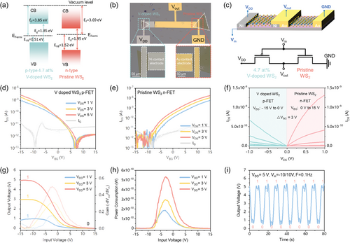
The homogeneous CMOS inverter was then constructed on a SiO2 (50 nm)/Si substrate by transferring a pristine monolayer WS2 domain and a 4.7 at% V-doped WS2 domain. For electrical measurements, Au and Ni were selected as the contact electrodes to inject electrons and holes into the n-type pristine WS2 and p-type 4.7 at% V-doped WS2, respectively. Figure 5b depicts an optical microscope image of a representative V-doped/pristine WS2 homogeneous CMOS inverter. The channel geometry was fine-tuned to attain symmetric voltage transfer characteristics (VTC) and for a balanced inverter (Wp = 6 µm and Wn = 10 µm). The schematic (top) and electrical configuration (bottom) of the homo-CMOS inverter are depicted in Figure 5c, comprising a n-type pristine WS2 FET and a p-type 4.7 at% V doped WS2 with a shared back gate. In the configuration of the homo-CMOS inverter, the input voltage (Vin) was applied to the common back gate, while the connected drains acted as the output voltage (Vout). The p-FET source was biased at the supply voltage (VDD), and the n-FET source was biased at the ground (GND). Figure 5d,e present the transfer characteristics (IDS–VBG) of the p-channel and n-channel FETs integrated into the CMOS inverter, operating at drain voltages of 1, 3, and 5 V, respectively. In Figure 5f, the output characteristics (IDS-VDS) of the two optimized FETs demonstrate ohmic-like behavior at low drain voltage and distinct saturation current trend at relatively high drain voltage.
The VTC and voltage gain curves of the homogeneous CMOS inverter are illustrated in Figure 5g for different VDD values of 1, 3, and 5 V. When Vin was −15 V, the V-doped WS2 p-FET activated while the pristine WS2 n-FET deactivated, causing Vout to rise to VDD (high-level logic “1”). Conversely, when Vin equaled 15 V, the V-doped WS2 turned off, and the pristine WS2 n-FET turned on, suppressing Vout to GND (low-level logic “0”). The voltage gain, represented as (-dVout/dVin), was determined from the associated VTC curves. The power consumption of the CMOS inverter, expressed as Power = VDD*IDD, is subject to the supply voltage, as illustrated in Figure 5h. A peak power consumption of 600 pW was observed at 5 V (performance regime). Additionally, static power consumption of approximately sub-5 pW was achieved under various supply voltages. Further, to assess the applicability of the ultrathin homogeneous CMOS inverter, we examined its dynamic switching behavior using a square wave ranging from −10 to 10 V under a VDD of 2 V at a frequency of 0.1 Hz, as illustrated in Figure 5i. A response delay of approximately 2s was observed at 0.1 Hz for these digital CMOS operations, likely attributed to the source/gate (S/G) overlap capacitance and inevitable contact resistance in both p- and n-FETs.[19] The lower operating frequency may be ascribed to the large device area and high parasitic capacitance resulting from the overlap of the gate and drain.[62, 63] With the aim of practical applications in mind, the current performance of our fabricated homogeneous CMOS inverter may not be competitive. However, it is crucial to emphasize that, for the first time, we have achieved the construction of a monolayer homogeneous CMOS inverter based on atomic substitutional doping in TMDs. This represents a milestone, and the device performance can be further enhanced through device size scaling and the implementation of a top gate structure.[64]
3 Conclusion
In summary, we demonstrate a CVD method for preparing monolayer WS2 films with lattice substitutional doping of V atoms using liquid-phase reaction precursors. As a kind of p-type dopant, V atoms were systematically introduced into the WS2 lattice, successfully achieving continuous and effective modulation of WS2 electrical polarity from intrinsic n-type to ambipolar, then to p-type, and ultimately to a quasi-metallic state with the gradually increasing doping ratio. The transition of WS2 from semiconductor to quasi-metallic state is attributed to the lattice phase transition (from 2H to 1T) induced by high-ratio V atom doping. FET devices were also successfully fabricated based on the prepared pristine and differently doped WS2 samples, exhibiting excellent and stable electrical performance. Notably, the V-doped monolayer WS2 with a 4.7 at% doping ratio showed outstanding p-type FET performance, with a switching ratio of ≈105. Capitalizing on this achievement, we ventured into unexplored territory by successfully crafting the inaugural prototype of a monolayer homogeneous CMOS inverter device through atomic substitutional doping in TMDs. These results affirm the potential for creating stable CMOS devices through the atomic doping in 2D materials, marking a significant milestone in the future development of integrated circuits.
4 Experimental Section
Synthesis of V-Doped (and Pristine) Monolayer WS2 via CVD
The precursor solution, serving as a source for W and V atoms, was prepared by blending aqueous solutions of AMT (NH4)6H2W12O40•xH2O, Aladdin, W source), AMV (NH4VO3, Aladdin, V source), and NaOH (Aladdin, promoter for monolayer growth). Initially, 0.1 grams of AMT, 0.1 grams of AMV, and 0.1 grams of NaOH are individually dissolved in 5, 10, and 20 mL of deionized (DI) water. These components were then harmoniously combined in a 1:1:1 volume ratio, resulting in a mixed precursor solution. The ratio of V atoms in monolayer V-doped WS2 was fine-tuned by adjusting the AMV content in the precursor solution. Following this, O plasma treatment was applied to augment the hydrophilicity of the SiO2 (270 nm)/Si substrate. The precursor solution was precisely spin-coated onto the surface of the pretreated SiO2/Si substrate at 3000 rpm for 1 min. Subsequently, another SiO2/Si substrate was delicately positioned face-to-face with the substrate coated with the precursor solution, creating the confined space essential for the growth of monolayer V-doped WS2. The SiO2/Si substrate was then situated at the center of the downstream temperature zone in a dual-temperature CVD chamber. Utilizing a quartz boat, 100 mg of sulfur powder was placed in the upstream temperature zone. The chamber is thoroughly purged with 100 sccm of Ar gas, and the upstream temperature was gradually elevated to 220 °C, followed by a subsequent increase in the downstream temperature to 800 °C, maintaining this temperature for 20 min. Subsequently, the chamber was allowed to naturally cool to room temperature.
Characterization
The topological morphologies of the pristine and V-doped monolayer WS2 were characterized by Optical Microscopy and AFM (Dimension Icon, Bruker), respectively. The Raman spectra and the mapping images were collected by a confocal microscope spectrometer (Alpha 300R, WITec, 532 nm laser with a power of 2 mW). The XPS were characterized using an X-ray Photoelectron Spectrometer (ESCALAB XI+ X-ray Photoelectron Spectrometer, Thermo Fisher). The atomic structure and V atom doping ratio were characterized by HAADF-STEM (JEM-ARM300F2, JEOL, 80 kV). The band structure of pristine (n-type) and V-doped (p-type) monolayer 2H-WS2 were characterized by the combination of PL and UPS spectra collected by confocal microscope spectrometer (Alpha 300R, WITec, 532 nm laser with a power of 2 mW) and X-ray Photoelectron Spectrometer (ESCALAB XI+ X-ray Photoelectron Spectrometer, Thermo Fisher, He I resonance line with wavelength 584 Å and photon energy 21.22 eV), respectively.
Device Fabrication and Measurements
All the pristine and V-doped monolayer WS2 FET devices with different doping ratios were fabricated on a SiO2(50 nm)/Si substrate. The source/drain contact electrodes, defined through a standard laser direct writing process, were crafted from 50 nm Au with 4 µm width of the channels. The homogeneous CMOS inverter was constructed on a SiO2(50 nm)/Si substrate, utilizing the substrate as the input (Vin) in the CMOS inverter configuration. The n-type pristine WS2 and p-type 4.7 at% V-doped WS2 were transferred onto the SiO2/Si substrate through the polymethyl methacrylate (PMMA)-assisted wet transfer method. Following this, metal electrodes were defined using a laser writing photolithography system. For the pristine n-FET, Au contact electrodes with a thickness of 50 nm were deposited through thermal evaporation. In contrast, Ni contact electrodes with a thickness of 50 nm were employed for the V-doped p-FET using an electron-beam evaporator. All electronic characteristics were systematically evaluated using an Agilent 4155C semiconductor parameter analyzer and a standard electrical probe station. These measurements were conducted under dark conditions and at room temperature.
Statistical Analysis
Acknowledgements
This research was financially supported by a fellowship award from the Research Grants Council of the Hong Kong Special Administrative Region, China (CityU RFS2021-1S04), the Shenzhen Municipality Science and Technology Innovation Commission (grant no. SGDX2020110309300402, the “‘Modulation and Detection of Terahertz Waves based on Semi-Metallic Two-Dimensional Materials,”’ CityU), the National Natural Science Foundation of China (52171014), and the Science, Technology and Innovation Commission of Shenzhen Municipality (JCYJ20210324134402007). [Correction added on June 28, 2024, after first online publication: Table 1 has been updated.]
Conflict of Interest
The authors declare no conflict of interest.
Open Research
Data Availability Statement
The data that support the findings of this study are available from the corresponding author upon reasonable request.


