Sulfide Chalcopyrite Solar Cells––Are They the Same as Selenides with a Wider Bandgap?
Abstract
Sulfide chalcopyrite solar cells are receiving renewed interest since they have reached a certified efficiency above 15%. Due to their wider bandgap, they are interesting candidates for top cells in tandem applications. They share many properties with the much deeper studied selenide chalcopyrites, but also some important differences. While the structure of shallow and deep defects appears very similar, the phase diagram is different with a much smaller existence range of Cu-poor CuInS2. The problematic character of the surface of material grown under Cu excess is present in both sulfides and selenides. Both materials show increased tail states when grown Cu-poor. To achieve sufficient bulk quality of sulfide absorbers, higher growth temperatures and a higher supply of sodium appear to be necessary.
1 Wide Bandgap Chalcopyrites as Top Devices in Tandem Solar Cells
The photovoltaics (PV) market today is almost entirely based on Si solar cells, with a share of around 5% of Cu(In,Ga)Se2 and CdTe-based solar cells.[ 1 ] These single-junction solar cells have reached record efficiencies in laboratories that are approaching theoretical and practical limits.[ 2 ] The cost of solar modules has decreased dramatically throughout the past decade to a point, where now the balance of system cost is higher than the cost of modules themselves.[ 1 ] As a result, the levelized cost of electricity is the lowest for PV plants, even including battery storage, compared to any other new power station.[ 3 ] This also means that cheaper PV-generated electricity is only possible if the efficiency is increased. However, for considerable increases in efficiency, new concepts will be needed. A promising approach is tandem solar cells.[ 4, 5 ] Bottom cells in tandem cells are typically Si solar cells[ 6, 7 ] or Cu(In,Ga)Se2 solar cells,[ 7-10 ] usually combined with perovskite top cells. Top cells need a bandgap between 1.6 and 1.9 eV,[ 11-14 ] high transparency for photons with energies below their bandgap and efficiency above 15%.[ 15, 16 ] And, of course, the efficiency must be stable. A material that has recently gained renewed interest is sulfide chalcopyrite Cu(In,Ga)S2. The best efficiency reported so far is 15.5%.[ 17 ] High deposition temperature and a Cu-poor composition have been listed as key factors allowing high efficiency.[ 18 ] A 15.2% efficient device has been demonstrated by our lab (in-house measurement).[ 19 ] The main factors enabling high efficiency were the reduction of bulk recombination by a Cu-poor composition and the reduction of interface recombination by a suitable buffer.[ 19 ] Additional buffer optimization led to a 14.0% solar cell, externally certified.[ 20 ] A 14.2% efficient device with a high bandgap of 1.65 eV, using a CdS buffer, has been reported.[ 21 ] These devices have a Mo back contact and can thus only be considered the first step toward a top cell for a tandem device. But it is certainly worthwhile to continue this journey, since chalcopyrite solar modules have shown stability over many years in field tests (see e.g., Ref. 22 or the specifications of module producers) and since they allow to adjust the bandgap in a wide range, interesting for top cells in tandem configurations. Another reason to study sulfide chalcopyrites is the fact, that the record chalcopyrite device is based on a sulfo-selenide absorber.[ 23 ] In this review, we compare sulfide chalcopyrites to the selenide compounds, which are much better studied, lay out the various steps that have been taken to reach efficiencies around 15%, and take an outlook on the next steps needed to demonstrate sulfide chalcopyrite solar cells as a top device in tandem solar cells.
2 Phase Diagram and Solar Cell Overview
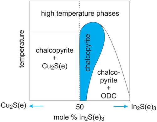
All Cu(In,Ga)(S,Se)2 chalcopyrites show different properties when prepared under Cu-rich or Cu-poor conditions. Pseudobinary phase diagrams of the ternary compounds have been determined early on and show a similar behavior, at least for CuInSe2, CuGaSe2, and CuInS2.[ 24-26 ] A schematic phase diagram, that applies to these chalcopyrites, is shown in Figure 1 . Chalcopyrite crystals exist under considerable Cu deficit, whereas material grown under Cu-excess results in a two-phase system, consisting of the stoichiometric or near-stoichiometric chalcopyrite and a Cu selenide or sulfide phase. CuGaS2, in contrast, was found to exist in the chalcopyrites phase even for Cu-rich compositions.[ 27, 28 ] For CuInSe2, it was shown by neutron scattering that the Cu-poor phase is stabilized by Cu vacancy and by In-on-Cu antisite defects.[ 29 ] A newer phase diagram of Cu(In,Ga)S2 found a very small existence region of Cu-poor CuInS2 [ 30 ] (see Section 4.3). In this contribution, we discuss also the differences between Cu-rich and Cu-poor chalcopyrite. By Cu-poor, we mean chalcopyrite with a Cu/(In + Ga) atomic ratio <1. By Cu-rich, we mean material that was grown under Cu-excess, which results in a two-phase situation: the Cu sulfide or selenide phases can be etched,[ 31-33 ] leaving the stoichiometric chalcopyrite. A discussion of Cu-rich versus Cu-poor Cu(In,Ga)Se2 can be found in .[ 34 ] Cu(In,Ga)Se2 and Cu(In,Ga)S2 have been investigated over the whole Ga/(Ga + In) composition range and no indication has been found for a miscibility gap.
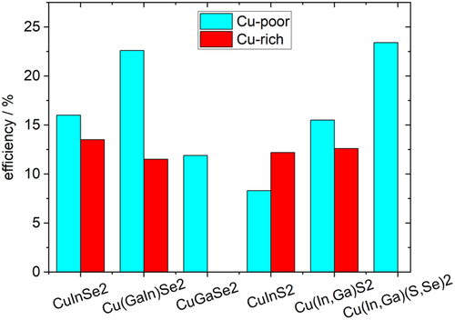
Solar cells have been made from Cu-rich (and etched) absorbers and from Cu-poor absorbers. Table 1 and Figure 2 show the best reported efficiencies for the different material systems. It can be seen that for all systems, except pure CuInS2 (without Ga), the Cu-poor absorbers perform better than the Cu-rich ones.
| Absorber | Details | Performance | Ref. |
|---|---|---|---|
| CuInSe 2 |
Cu-poor Three-stage co-evaporation KF-PDT, heat treatment AR coating |
Certified η = 16.0% V OC = 526 mV J SC = 41.0 mA cm−2 FF = 74.4% |
122 |
| CuInSe2 |
Grown Cu-rich One-stage coevaporation In–Se surface treatment |
In house η = 13.5% V OC = 470 mV J SC = 42.2 mA cm−2 FF = 68% |
[76] |
| Cu(In,Ga)Se2 |
Cu-poor Multistage coevaporation RbF-PDT AR coating |
Certified η = 22.6% V OC = 741 mV J SC = 37.8 mA cm−2 FF = 80.6% |
110 |
| Cu(In,Ga)Se2 |
Grown Cu-rich Three-stage coevaporation Ga–Se surface treatment |
In house η = 11.5% V OC = 589 mV J SC = 29.8 mA cm−2 FF = 67% |
[94] |
| CuGaSe2 |
Cu-poor Three-stage coevaporation AR coating |
In house η = 11.9% V OC = 1017 mV J SC = 17.5 mA cm−2 FF = 67% |
123 |
| CuInS2 |
Cu-poor One-stage coevaporation |
In house η = 8.3% V OC = 613 mV J SC = 20.5 mA cm−2 FF = 66% |
68 |
| CuInS2 |
Grown Cu-rich One-stage coevaporation AR coating |
In house η = 12.2% V OC = 742 mV J SC implied from QE FF = 70.8% |
[80] |
| Cu(In,Ga)S2 |
Cu-poor Sequential from metallic precursor AR coating |
Certified η = 15.5% V OC = 920 mV J SC = 23.4 mA cm−2 FF = 72.2% |
17 |
| Cu(In,Ga)S2 |
Grown Cu-rich Sequential from metallic precursor AR coating |
Certified η = 12.6% V OC = 879 mV J SC = 20.4 mA cm−2 FF = 70% |
[69] |
| Cu(In,Ga)(S,Se)2 |
Cu-poor Sequential from metallic precursor CsF-PDT AR coating |
Certified η = 23.4% V OC = 734 mV J SC = 39.6 mA cm−2 FF = 80.4% |
23 |
3 Electronic Defects
The electronic bulk defects in a solar cell absorber play a decisive role in its usability in a solar cell. Shallow defects determine the doping level, whereas deep defects present detrimental recombination centers. The electronic defects in Cu(In,Ga)Se2 have been studied in detail experimentally and theoretically. A review can be found in Ref. 35. The p-type nature of the material is mostly due to two dominating shallow acceptors: the Cu vacancy and the CuIII antisite (III = In or Ga), which are partly compensated by shallow (Cui and InCu antisite) and deep (GaCu antisite) donor defects. Another deep defect is consistently observed at 0.8 eV independent of the Ga content. However, its nature is still unclear.
3.1 Shallow Defects
Experimental information on the defects in Cu(In,Ga)Se2 and Cu(In,Ga)S2 comes to a large part from low-temperature photoluminescence (PL) measurements on material grown under Cu-excess, i.e., the chalcopyrite is stoichiometric.[ 35 ] In general, spectroscopy of shallow defects is not possible in Cu-poor selenide chalcopyrite: Cu-poor Cu(In,Ga)Se2 is compensated, mostly by the combined occurrence of InCu donor defects and VCu acceptor defects.[ 29, 36, 37 ] This compensation leads to fluctuating electrostatic potentials, which broaden and red-shift the low-temperature PL emissions.[ 38-41 ] These broad emissions render spectroscopy of shallow defects impossible. Whether sulfide chalcopyrites show the same broadening when grown Cu-poor, is not finally clarified at the moment, since no PL measurements on material with a Cu/In or Cu/Ga ratio <0.9 have been reported. The reason might be the narrow existence region of Cu-poor CuInS2, as discussed in Section 4.3. The observation of tail states in Cu-poor sulfides (see Section 4.4) supports the assumption that Cu-poor sulfides are also compensated. In contrast to Cu-poor, the low-temperature PL spectra of CuInSe2 [ 41 ] and CuGaSe2 [ 40 ] grown under Cu-excess are dominated by two donor–acceptor pair transitions, which start from the same shallow donor (InCu antisite or Cui interstitial). They involve the two main acceptors: the shallower one (VCu), which leads to the higher energy PL emission (DA1), dominating near stoichiometric compositions and the somewhat deeper one (CuIn) becoming dominant as the Cu-content increases, leading to a somewhat lower energy PL emission (DA2). The attribution of electronic defects to a certain defect chemistry has been based on compositional trends and mostly on comparison with state-of-the-art calculations.[ 35 ]
A similar behavior of the low-temperature PL is found in Cu-rich sulfides CuInS2 [ 42, 43 ] and CuGaS2.[ 44-46 ] The spectra observed in CuInS2 follow exactly the same pattern as observed in selenide chalcopyrites: they are dominated by two donor–acceptor pair transitions, which involve the same shallow donor and two different acceptors, where again the shallower (involved in DA1) dominates for near stoichiometric compositions and the somewhat deeper one (involved in DA2) increases with higher Cu-content.[ 42 ] Composition-dependent experiments[ 47 ] and first-principle calculations[ 19, 48 ] identify VCu as the most shallow acceptor, followed by CuIn. Thus, it appears that the two dominating acceptors in sulfide and in selenide chalcopyrite are the same. Cui has been found as a shallow donor.[ 48 ] The same study also presents InCu as a shallow donor, whereas other calculations find InCu to be a deep donor.[ 19, 49 ] The shallow donor has also been attributed to the sulfur vacancy,[ 50 ] which could be supported by the fact that CuInS2 grown or annealed under a low S atmosphere has been observed to be n-type.[ 51, 52 ] A second shallow donor that was reported in earlier experiments could be identified as a phonon replica[ 42 ] Two shallow donor–acceptor pair transitions are also observed in CuGaS2, which have been identified as due to one shallow donor and two shallow acceptors, however, the composition dependence does not follow the same pattern: The (higher energy) DA1 is observed up to a Cu/Ga ratio of 2.0 and the ratio between the two peaks does not show a characteristic composition dependence.[ 46 ] For both In compounds (sulfide[ 42 ] and selenide[ 41 ]), the DA2 transition becomes dominant already at a very low Cu excess of a few percent, whereas in CuGaSe2 the DA2 becomes dominant only beyond a Cu/Ga ratio of 1.1[ 40 ] and in CuGaS2 no clear trend with composition between the intensities of the two DA transitions has been observed. All compositions were determined by energy dispersive X-Ray spectroscopy (EDX). Considering the error in EDX, it remains unclear whether the difference in trend between CuInSe2/CuInS2 and CuGaSe2 is significant or not.
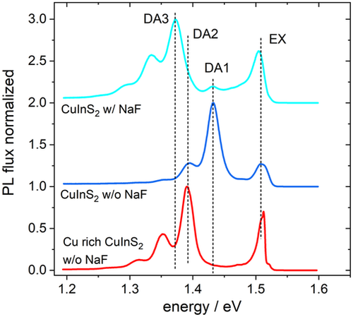
A third shallow acceptor was found in polycrystalline CuInSe2 grown by coevaporation on glass, covered with Mo.[ 53 ] It was identified as the In vacancy and seems to be favored by the high Se pressure present in the coevaporation process, which can be attributed to the lower formation energy of the In vacancy at high Se pressure.[ 37 ] A similar defect is found in CuInS2, however not with an increase in Se pressure but with an increase in Na content. Figure 3 shows low-temperature PL spectra of CuInS2 films. The red and the dark blue line depict the typical spectra[ 42 ] for Cu-rich (red) and for near stoichiometric (dark blue) CuInS2: both show an excitonic emission near 1.51 eV (EX). The Cu-rich material is dominated by the DA2 transition at 1.39 eV and the near-stoichiometric one by the DA1 transition around 1.43 eV. The light blue spectrum is measured on a sample that was grown in the same process as the near-stoichiometric one, but the substrate, in this case, was covered by a thin NaF film. The spectrum also shows the excitonic emission and the DA1 emission, but in addition another DA emission at 1.37 eV, which we label DA3. Its phonon replicas are clearly visible towards lower energies with the same 39 meV distance as the phonon replicas of DA1 and DA2. Furthermore, the flux distribution can be nicely fitted by a Huang-Rhys distribution[ 54, 55 ] (see Figure S1, Supporting Information). The DA nature is confirmed by a slight blue shift of 3.8 meV per decade with increasing excitation intensity, together with a power-law exponent of the intensity that starts out at 1 and becomes ½ at higher excitations (see Figure S2, Supporting Information). This change in the power-law behavior is exactly what is expected of a DA transition that is energetically between another one.[ 56 ] From the free-to-bound transition observed at 80 K (Figure S3, Supporting Information), the third acceptor can be placed at (170 ± 5) meV above the valence band.
In CuInSe2, it was found that the appearance of the third acceptor is linked to sufficient Se pressure during growth.[ 53 ] In CuInS2, it seems that Na enhances the third acceptor. This raises the question if the Se-dependent behavior in CuInSe2 is actually due to the enhanced transport of Na in the presence of Se.[ 57 ] Further investigations are needed to clarify which growth conditions strengthen the A3 acceptor in CuInSe2 and CuInS2.
A third DA transition has also been observed in some CuGaSe2 films, grown under low Se supply and without Na, however, its nature is unclear.[ 35 ] CuGaS2 films show a third DA transition, with an increasing intensity with an increasing Cu/Ga ratio.[ 46 ] Thus, it appears that all Cu(In,Ga)(S,Se)2 chalcopyrites show a third shallow acceptor, although it is not clear whether all “A3” acceptors have the same defect chemistry.
In summary, the shallow defects in CuInSe2, CuGaSe2, CuInS2, and CuGaS2 are very similar. All four materials feature three shallow acceptors and one shallow donor. The observed defects and their low-temperature PL transitions are summarized in Figure 4 and Table 2 . It is interesting to note that the shallow donor has an energy of around 10 meV in both selenides (CuInSe2 and CuGaSe2), whereas it is found at around 30 meV in both sulfides (CuInS2 and CuGaS2). The acceptors become deeper when replacing Se with S. In the selenides, the three shallow acceptors become deeper when replacing In with Ga, in agreement with the expectations from the hydrogen-like defect model.[ 58 ] There is no clear trend with Ga addition in the sulfides: the two most shallow acceptors are deeper in CuInS2 than in CuGaS2, whereas the third acceptor is deeper in CuGaS2 than in CuInS2. Not only are the doping defects similar in selenide and sulfide chalcopyrites, also the observed doping levels are similar: in Cu-poor Cu(In,Ga)S2 the net doping has been observed in the range of several 1015–1016 cm−3, whereas Cu-rich Cu(In,Ga)S2 shows a net doping in the low 1017 cm−3 range.[ 19, 59, 60 ]
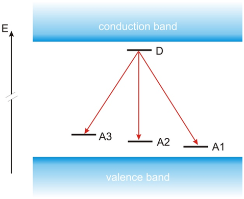
| D | A1 | A2 | A3 | DA1 | DA2 | DA3 | |
|---|---|---|---|---|---|---|---|
| CuInSe2 | 0.01 | 0.040 | 0.060 | 0.135 | 0.99 | 0.97 | 0.90 |
| CuInS2 | 0.03 | 0.105 | 0.145 | 0.170 | 1.42 | 1.38 | 1.36 |
| CuGaSe2 | 0.01 | 0.060 | 0.100 | 0.130 | 1.65 | 1.62 | 1.57 |
| CuGaS2 | 0.04 | 0.065 | 0.085 | 0.215 | 2.41 | 2.38 | 2.29 |
3.2 Deep Defects
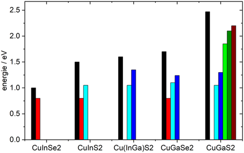
The shallow defects, discussed in Section 3.1, are responsible for the doping behavior of Cu(In,Ga)(S,Se)2 absorbers. For the performance of these materials in solar cells, deep defects play a decisive role since they act as recombination centers and lead to nonradiative recombination, which decreases the open-circuit voltage of the solar cell.[ 61-63 ] In general, wide bandgap semiconductors are more likely to show deep defects. Many deep defects tend to remain at the same absolute energy, see, e.g.,.[ 35, 64, 65 ] Thus, defects that are shallow in narrow bandgap semiconductors can become deep in wide-gap semiconductors. An example is the GaCu antisite defect in the selenide chalcopyrites, which is deep in CuGaSe2 and becomes shallow with the addition of In below a Ga/(Ga+In) ratio of about 0.5.[ 35 ] This defect is responsible for the PL transition in Cu(In,Ga)Se2 at 1.1 eV.[ 35, 66 ] Additionally, one deep defect with an energy around 0.7–0.8 eV has been observed in almost all chalcopyrites: in CuInSe2 and CuGaSe2,[ 35 ] in Cu(In,Ga)Se2 [ 67 ] and in CuInS2. [ 50, 68 ] In Cu(In,Ga)S2 and CuGaS2 it could be present, but hidden by a very strong emission around 1.05 eV. In Cu(In,Ga)Se2, the 0.8 eV defect appears to be more prominent in Cu-rich material.[ 35 ] In CuInS2, it was observed that higher growth temperatures help to reduce this deep defect and at the same time increase the quasi-Fermi level splitting.[ 68 ] In CuInS2, the most prominent deep defect emission is seen at 1.05 eV in the PL spectra.[ 68 ] A similar emission in Cu(In,Ga)S2 has been detected in Cu-rich films, but is reduced with decreasing Cu content.[ 19 ] This defect has been related to the open-circuit voltage (V OC) loss.[ 19 ] An additional emission of around 1.35 eV in Cu(In,Ga)S2 is also reduced with lower Cu content of the films.[ 19 ] Three additional deep defect transitions are observed in CuGaS2 at energies of 1.8, 2.1, and 2.2 eV.[ 46 ] The attribution of electronic defects to the defect chemistry is currently much less clear in sulfides than in selenides. An overview of the deep defect transitions observed by PL in the various chalcopyrites is given in Figure 5 . It is important to note that these are the PL emission energies, not the defect energies. And most likely these deep defect transitions are influenced by phonon interactions and do not represent the zero-phonon lines.[ 35 ] To identify defect energies and defect chemistries, more detailed PL investigations and also defect calculations are necessary. But the observed PL transitions give an indication of the presence of deep defects. It appears, that similar deep defects are present in all Cu(In,Ga)(S,Se)2 chalcopyrites. The 0.8 eV transition has not been observed in Cu(In,Ga)S2 and CuGaS2, however, it could just be hidden under the very strong emission of around 1.05 eV. As expected, it is observed that with a wider bandgap, more deep defects appear. These defects are likely also present in the narrower bandgap compounds, but there they are shallow defects, just like the GaCu antisite defect in Cu(In,Ga)Se2.[ 35 ]
4 Cu-Rich Versus Cu-Poor
Originally, CuInS2 solar cells were prepared with absorbers grown under Cu excess, because of secondary phases in the Cu-poor material.[ 33 ] Before 2015, the best efficiency was reached with the addition of Ga, still using absorbers grown under Cu excess.[ 69 ] However, the current record solar cell with an efficiency of 15.5%[ 17 ] and all reported Cu(In,Ga)S2 solar cells with efficiencies around 15%[ 19-21, 70 ] are prepared from Cu-poor absorbers. The difference is attributed to the fact that Cu-rich solar cells are dominated by interface recombination.[ 60, 68, 71, 72 ]
4.1 The Cu-Rich Surface
The same observation has been made for the selenide chalcopyrites:[ 34 ] lower efficiencies, in particular, lower open-circuit voltages are obtained with Cu-rich absorbers, which is due to interface recombination.[ 71 ] It was only recently shown what causes this interface recombination in the selenide chalcopyrites: it is due to a defect that appears around 200 meV activation energy in admittance spectra,[ 73 ] which is caused by the combined effect of oxidation and the necessary etching step in Cu-rich material.[ 74 ] This effect can be traced back to the behavior of Cu(In,Ga)Se2 when exposed to atmospheric oxygen (see Figure 6 ): when Cu(In,Ga)Se2 is oxidized, the first to form is the group III oxide (see Ref. 74 and references therein as well as Ref. 75 for the Ga compound). This means that group III atoms are removed from the chalcopyrite phase, making the chalcopyrite more Cu-rich or less Cu-poor. This is no problem in Cu-poor material since it will just move somewhat closer to stoichiometry. However, the stoichiometric chalcopyrite that results from a Cu-rich growth will necessarily cross the boundary in the phase diagram and will form Cu2Se. To form this phase, Se atoms will be removed from the chalcopyrite phase, creating Se vacancies. This defect or a related defect complex is the cause of the 200 meV admittance signal.[ 73 ] This model is corroborated by the observation that annealing in Se-containing atmosphere removes or reduces this defect and improves the V OC.[ 73 ] Furthermore, the V OC loss can be completely recovered by a treatment with In and Se.[ 76, 77 ] The defect was shown to reside in a thin layer (a few tens of nm thick) just below the absorber surface.[ 78 ] Modeling shows that such a layer results in the typical signatures of interface recombination: activation energy of the reverse saturation current lower than the bandgap and a V OC considerably smaller than the quasi-Fermi level splitting.[ 78 ]

The question arises if a similar mechanism causes the interface recombination in Cu-rich sulfide chalcopyrites. So far, it has not been possible to detect a corresponding defect signature in admittance spectroscopy on Cu-rich CuInS2 or Cu(In,Ga)S2 devices, because the spectra are dominated by the high doping level in Cu-rich absorbers.[ 19, 59 ] However, it was shown that the interface V OC loss, i.e., the difference between V OC (times unit charge) and quasi-Fermi level splitting, in Cu-rich CuInS2 solar cells is reduced by S treatment[ 79 ] or by using buffers which are prepared from solutions with a high sulfur concentration.[ 80 ] This observation, together with the similarity in the phase diagrams, suggests that a similar mechanism is active in Cu-rich sulfide chalcopyrites: defects related to the S vacancy are likely caused by oxidation and etching and cause the loss in V OC due to near-interface recombination.
To summarize this comparison: Cu-rich growth leads to interface recombination in both sulfide and selenide chalcopyrite solar cells, which can be attributed to a defective layer just below the surface containing defects related to chalcogen vacancies.
4.2 Bulk Quality
Although the interface of Cu-poor CuInS2 solar cells is superior, its bulk has been found to be of lower quality. The electronic quality of the bulk is assessed by the quasi-Fermi level splitting (qFls), determined from absolute PL measurements of the absorber, before finishing the solar cell.[ 63 ] It should be mentioned that selenide chalcopyrites degrade quickly in air, in particular under laser illumination.[ 81-83 ] Therefore, absorbers are covered with a thin CdS layer, which prevents degradation and maintains the qFls of the fresh absorber.[ 82, 83 ] On the contrary, the qFls measured in sulfide chalcopyrites are stable over days, allowing to measure the qFls of sulfide absorbers without the CdS buffer.[ 84 ] This has been observed for Cu-rich and Cu-poor absorbers alike.[ 84 ] Since the qFls depend on the bandgap, it is better to compare the qFls loss, which is defined as the difference between the ideal Shockley–Queisser open-circuit voltage (times the unit charge) and the measured qFls: . The bandgap to determine should be taken as the PV bandgap, determined from the inflection point of the external quantum efficiency (EQE) spectrum of the short-circuit current[ 85 ] or the absorptance spectrum.[ 86 ] Figure 7 gives an overview of how the qFls loss depends on the Cu/In or Cu/(In+Ga) atomic ratio. The qFls loss values are based on qFls values determined from a fit to generalized Planck's law, keeping the temperature in the fit to the measurement temperature.[ 63 ] For the CuInS2 samples is determined from the PV bandgap, corresponding to the inflection point of the EQE spectrum. Since we do not have EQE (or even solar cells) of all samples, we use the typical values for the bandgap (see also Figure 9): 1.506 eV for all Cu-rich films, 1.475 eV for 1-stage Cu-poor films, and 1.490 eV for multi-stage Cu-poor films. For the CIGSe samples, already reported in Ref. 19 we used the PL maximum for the bandgap, this may underestimate the qFls loss somewhat (on the order of 10–20 meV).[ 63 ] For the new data (Cu-poor Cu(In,Ga)S2), the qFls loss was directly determined from the radiative efficiency (Y PL) according to –kT lnY PL.[ 63, 86 ] Concerning the CuInS2 samples, we can see that at least for Cu-rich material, higher growth temperatures are beneficial.[ 68 ] In the literature, an inprovement with higher growth temperature has also been observed in Cu-poor absorbers.[ 18 ] Furthermore, the qFls loss in Cu-poor CuInS2 absorbers is observed to be higher than in Cu-rich absorbers.[ 68, 87 ] This is seen on soda-lime glass[ 68 ] (full symbols in Figure 7) with a relatively high content of Na, as well as on a low-Na high-temperature glass (open symbols in Figure 7).[ 87 ] Though, it should be noted, that in both studies the Cu-poor films were grown in a single-stage process (circles in Figure 7) and had rather small grains.[ 68 ] Recent experiments with Cu-poor absorbers grown by a three-stage process (green stars in Figure 7) indicate a considerable reduction of the qFls loss in Cu-poor CuInS2, but still, the Cu-rich absorbers perform better by about 40 meV. It appears that a multistage process is not beneficial for Cu-rich CuInS2 but improves the qFls in Cu-poor material considerably. Still, even when comparing the best processes for Cu-rich and Cu-poor CuInS2 and the same growth temperatures, Cu-poor CuInS2 is of lower quality than Cu-rich material from the viewpoint of bulk material.
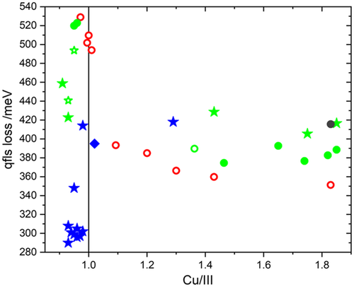
The situation is different when considering Cu(In,Ga)S2 with Ga added (blue symbols in Figure 7). In that case, the Cu-poor multistage films show lower qFls loss compared to any Cu-rich Cu(In,Ga)S2 [ 19 ] and compared to any Cu-poor CuInS2. The comparison between Cu-rich and Cu-poor Cu(In,Ga)S2 (with Ga) is similar to what is observed in Cu(In,Ga)Se2: qFls loss is higher in Cu-rich Cu(In,Ga)Se2 than in Cu-poor Cu(In,Ga)Se2 when comparing the same bandgaps,[ 83 ] and the difference increases with increasing bandgap.[ 35 ] This observation can be attributed to a deep defect. One could suggest that it is the defect responsible for the 0.8 eV emission in Cu(In,Ga)Se2 [ 35 ] and possibly the defect responsible for the emission of around 1.05 eV in Cu(In,Ga)S2 [ 19 ] that are both more prominent in Cu-rich material and become deeper, i.e., closer to midgap, when the bandgap increases. Defects around midgap are the most effective for nonradiative recombination. Alternatively, the lower quality of Cu-rich absorbers could be caused by the necessary etching step which damages the surface, as discussed earlier.
4.3 Existence Region and Segregation
The Cu-rich/Cu-poor comparison leads to different results in CuInS2 (better Cu-rich absorbers) than in Cu(In,Ga)S2 (better Cu-poor absorbers). Thus, the question arises why it is more difficult to prepare high-quality Cu-poor CuInS2 (without Ga), whereas high-quality films with an overall Ga/(Ga+In) atomic ratio of around 15% are possible.[ 19 ] The recently determined pseudo ternary phase diagram of the Cu2S–In2S3–Ga2S3 system[ 30 ] (Figure 8 ) might give an answer. In contrast to CuInSe2, where a wide existence region of the chalcopyrite phase is observed for Cu-poor material,[ 24, 88-90 ] the existence region of Cu-poor CuInS2 is very small: Cu deficiency leads almost immediately to the formation of a secondary phase with a cubic crystal structure.[ 30 ] This is in agreement with early reports that CuInS2 could not be prepared single phase:[ 33 ] Cu2-xS was always present in Cu-rich growth (but this phase stays at the surface and can be etched away) and In-rich phases were present in Cu-poor growth. However, the phase diagram in Figure 8 shows that the existence region on the Cu-poor side widens with increasing Ga content in Cu(In,Ga)S2. Thus, we propose the Ga-induced widening of the Cu-poor Cu(In,Ga)S2 existence region as an explanation for the different trends in bulk quality in CuInS2 and Cu(In,Ga)S2, comparing Cu-rich and Cu-poor material, and for the recent progress with Cu-poor material. As discussed in the previous section: for sulfides as for selenides, Cu-poor material is preferable for solar cells, because it avoids oxidation and etching-related surface damage. But in sulfide chalcopyrite, it is necessary to add Ga to allow Cu-poor compositions.
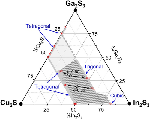
The phase diagram in Figure 8 implies another problem that concerns the growth of homogeneous Cu(In,Ga)S2: the black circles indicate the target compositions of the prepared material and the arrows indicate the phases that were obtained: a near stoichiometric chalcopyrite phase and a very Cu-poor cubic or trigonal phase. What is important to note is that the Ga content of the two phases is different: the Cu-poor phase is In richer than the near-stoichiometric phase. This difference seems to increase with increasing overall Ga content. These observations indicate that a growth process with a composition in the two-phase region will not only lead to segregation into phases with different Cu content but also with different Ga contents. This problem is particularly severe in a three-stage process, which starts from (In,Ga)2S3 and has to move through the two-phase region. Interestingly, the phase segregation does not occur in a homogeneous distribution of small grains but as a layered structure.[ 91 ] Segregation into Ga-rich and In-rich phases is, however, not limited to three-stage coevaporation processes, it was also observed in sequential processes that start with a metallic precursor, even in Cu-rich films.[ 92 ] The segregation leads to layers inside the absorber with a low Ga content and thus a low bandgap. Since the absorption edge depends on the lowest bandgap, this segregation is detrimental for high open-circuit voltages and for high bandgaps.[ 91 ] It appears, that overall lower Ga contents, leading to an absorption edge up to about 1.7 eV, and higher temperatures allow a better control of the Ga profile throughout the absorber depth.[ 18, 19, 21 ]
4.4 Tail States
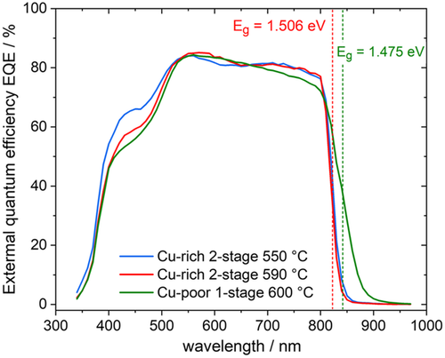
A distinct difference between Cu-rich and Cu-poor selenide chalcopyrites is the occurrence of electrostatic potential fluctuations and the correlated tail states in Cu-poor material, which is due to doping compensation. These tail states have been detected by low-temperature PL studies,[ 35, 93 ] by room temperature PL measurement, from which the absorption coefficient can be extracted,[ 34 ] and from the steepness of the EQE spectrum.[ 88 ] Cu poor Cu(In,Ga)Se2 has stronger potential fluctuations, more tail states, and a more gradual increase of absorption and EQE at the absorption edge. In fact, the steepness of the absorption edge in EQE spectra has been used as an indicator to distinguish between Cu-rich and Cu-poor material.[ 94 ] The same difference has been observed in CuInS2: Figure 9 shows the EQE spectra of the CuInS2 solar cells, which are discussed in Ref. 68. The onset of the Cu-poor cell is more gradual than that of the Cu-rich cells, even with lower growth temperature, indicating the same effect of tailing in sulfides as in selenides. It is important to note that the gradual onset, in this case, is not due to a bandgap gradient. These are pure CuInS2 films, without Ga and without bandgap gradient. The EQE spectra reported in Ref. 19 seem to contradict that statement, since the steepness of the onset does not vary between Cu-rich and Cu-poor cells. It has to be noted, however, that the most Cu-poor sample in Ref. 19 has still a higher Cu content than the Cu-poor sample in Figure 9, which has a Cu/In atomic ratio of 0.9. Also in selenides, the more gradual increase in EQE has been observed typically for samples with a Cu/III atomic ratio around or below 0.9.[ 88, 94 ] A broad asymmetric emission in low-temperature PL is also indicative of the appearance of potential fluctuations and the related tail states.[ 35 ] This signature appears in CuInSe2 at a Cu/In atomic ratio of 0.91 and below.[ 41 ] It is interesting to note that in CuGaSe2 the signature of potential fluctuations appears as soon as the material becomes Cu-poor.[ 40 ] In summary: both Cu-poor sulfides and Cu-poor selenides show tail states due to electrostatic potential fluctuations and a more gradual increase of EQE spectrum, compared to Cu-rich material.
5 Comparison of Loss Mechanisms in Solar Cells
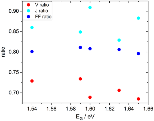
The best Cu(In,Ga)S2 solar cells show efficiencies of around 15%.[ 17, 19-21, 70 ] Figure 10 analyses their photovoltaic parameters as a ratio of the Shockley–Queisser parameter. The bandgaps are either given in the publication or inferred from the inflection point of the published EQE spectrum. It is obvious that the most critical parameter is the open-circuit voltage. Along with a V OC deficit goes always a reduction in the fill factor. The short circuit current is the least critical, as also becomes obvious from the EQE spectra of the best cells, which show maximum values around or above 90%.[ 19, 21 ] To improve V OC, it is important to study the various recombination losses in these solar cells.
5.1 Interface Recombination
As mentioned earlier, the early Cu(In,Ga)S2 solar cells, which were based on absorbers grown under Cu excess, were dominated by interface recombination, which reduces the open-circuit voltage.[ 80, 95, 96 ] Even the best Cu-rich Cu(In,Ga)S2 device is limited by interface recombination.[ 72 ] In this context, it is always the absorber–buffer interface that is concerned. Two main measurement methods are used to determine if interface recombination is the main loss mechanism: 1) extrapolation of the temperature dependence of V OC to determine the activation energy of the reverse saturation current. If the activation energy is smaller than the bandgap of the absorber, it can be assumed that interface recombination is the main loss channel.[ 95 ] 2) a significant difference between qFls and V OC also indicates severe interface recombination.[ 78 ] The difference is, therefore, labeled the interface V OC loss.
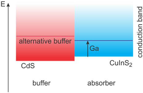
Interface recombination is caused by unfavorable band alignment, Fermi level pinning,[ 95 ] or a near-interface defective layer.[ 78 ] The band alignment is unfavorable if a cliff configuration exists, i.e., if the conduction band edge in the buffer or contact layer is below the one in the absorber. CdS is the buffer material used most often in Cu(In,Ga)(S,Se)2 solar cells.[ 97, 98 ] However, it has been shown to form a cliff already with CuInS2 without Ga.[ 99, 100 ] Similar to Cu(In,Ga)Se2,[ 101 ] it can be assumed that the addition of Ga shifts the conduction band in the absorber up, making the cliff even larger. The situation is illustrated in Figure 11 . In fact, a rather large cliff has been detected at the Cu(In,Ga)S2/CdS interface.[ 102 ] This can be mitigated by using buffers with a higher conduction band edge energy.[ 19, 72 ] ZnOS has been shown to form a spike with CuInS2 [ 103 ] and was also found to mitigate interface recombination in Cu-poor Cu(In,Ga)S2.[ 19 ] Other buffers that form a favorable interface with Cu-poor Cu(In,Ga)S2 have been shown to be ZnMgO[ 70 ] or ZnSnO.[ 20 ]
However, as discussed earlier, solar cells based on Cu-rich absorbers are always dominated by interface recombination, regardless of the buffer used.[ 19, 60, 72 ] Fermi-level pinning can be excluded based on photoemission spectroscopy, where interface-induced band bending is always observed.[ 102, 103 ] The reason for the dominating interface recombination in Cu-rich Cu(In,Ga)S2 has been discussed earlier: it is due to a defective layer near the surface of the absorber, with defects related to chalcogen vacancies generated by the oxidation behavior and the necessary etching step of the stoichiometric chalcopyrite obtained in Cu-rich growth. This cause of interface recombination can only be avoided by using Cu-poor absorbers. For Cu-poor absorbers containing Ga, CdS buffers may form a cliff; in this case, it is necessary to use an alternative buffer.[ 19, 20, 70, 104 ] All our best solar cells are based on Cu-poor absorber and show an activation energy of the saturation current equal to the bandgap[ 19 ] and an interface V OC loss around 20 meV or lower, if alternative buffers are used with a higher conduction band edge.[ 19, 20 ] It should be noted, though, that the Cu(In,Ga)S2 solar cell with a reported bandgap of 1.65 eV and using a CdS buffer is not dominated by interface recombination.[ 21 ]
5.2 Bulk Recombination
If the solar cell is dominated by bulk recombination, the open-circuit voltage will be similar to the quasi-Fermi-level splitting, measured by PL.[ 78, 105 ] Thus, Figure 7 can give insights into the bulk quality of sulfide absorbers. It should be noted though, that the back contact is generally present in PL measurements, hence, back surface recombination will be reflected by a reduced qFls as well.[ 106, 107 ] The best selenide absorbers show qFls losses below 130 meV,[ 108 ] whereas it can be seen from Figure 7 that even our best sulfide absorbers exhibit qFls losses more than twice as high. This goes along with the observation of a much shorter minority carrier lifetime in sulfides than in selenides: Cu-poor Cu(In,Ga)S2 shows lifetimes of a few ns,[ 19, 60 ] whereas selenide chalcopyrites show lifetimes about two orders of magnitude higher.[ 81, 109 ] A factor of 100 in the lifetime without a change in doping would decrease the V OC loss or quasi-Fermi-level splitting loss by 120 meV,[ 63 ] which is very close to the observed difference, as just discussed. This observation clearly indicates that the quality of sulfide solar absorbers needs to be improved. Several paths for improvement can be extracted from Figure 7. Multistage processes improve the quality of Cu-poor absorbers (comparing stars with circles in Figure 7). This is similar to the observations at selenide chalcopyrites: the best cells are prepared by a three-stage process[ 110, 111 ] or by a modified three-stage process.[ 112, 113 ] When comparing different growth temperatures in Figure 7 (high: red, medium: green and blue, low: grey) it appears that higher temperatures are beneficial for sulfide absorbers, as reported earlier.[ 18, 68 ] Finally, comparing open symbols (glass with lower Na content) and closed symbols (soda-lime glass) of the same color indicates that for Cu-poor absorbers a higher Na substrate is beneficial. On the Cu-rich side, the influence of Na appears negligible, as has been observed in the past.[ 114 ] Investigations of the influence of additional Na on Cu-poor Cu(In,Ga)S2 are underway. Preliminary results (see also Table 3 ) show a small positive influence of a NaF post-deposition treatment (PDT) in single-stage Cu-poor CuInS2, but a negative influence on the (better) absorbers from three-stage processes. A NaF precursor film, deposited on the Mo back-contact before the absorber growth, has a positive effect on CuInS2, but a negative one on Cu(In,Ga)S2. Codeposition of NaF during the second or third stage of the three-stage process has a clear positive effect with an increase in qFls of 80 meV. A qFls loss as low as 220 meV has been achieved by this method. In this case, qFls loss is determined directly from the radiative efficiency (Y PL) according to –kT lnY PL.[ 63, 86 ] These experiments were done on soda-lime glass.
| Absorber and growth process | Na process | Effect on qFls |
|---|---|---|
| CuInS2 single-stage | NaF-PDT | + |
| CuInS2 three-stage | NaF-PDT | − − |
| CuInS2 single stage | NaF precursor | + |
| CuInS2 three-stage | NaF precursor | + + [+40 meV] |
| Cu(In,Ga)S2 three-stage | NaF precursor | − − |
| Cu(In,Ga)S2 three-stage | NaF codepostion during the second or third stage | + + + [+80 meV] |
In Figure 7 we can also compare CuInS2 and Cu(In,Ga)S2. One important difference between CuInS2 and Cu(In,Ga)S2 absorbers is the presence of a Ga gradient in the latter,[ 19 ] in particular when grown by a three-stage process, same as in Cu(In,Ga)Se2.[ 115 ] The Ga gradient in Cu(In,Ga)Se2 absorbers has been shown to suppress backside recombination at Mo back contact.[ 107, 116 ] When comparing CuInS2 and Cu(In,Ga)S2, grown under the same conditions or single and multistage Cu(In,Ga)S2 (stars and diamonds) in Figure 7, there seems to be little influence of the Ga gradient in Cu-rich absorbers. In Cu-poor absorbers, the qFls loss in Ga-containing absorbers is clearly lower. A positive influence of a suitable Ga gradient in Cu-poor Cu(In,Ga)S2 has been reported earlier.[ 18 ] In selenide chalcopyrites, the exact Ga profile has been extensively optimized.[ 117, 118 ] As discussed in Section 4.3, the control of the Ga gradient might be more difficult in sulfides, because of its phase diagram (Figure 8).[ 91 ] However, the positive effect of Ga addition, obvious in Figure 7, could also be due to the larger existence region of Cu-poor Cu(In,Ga)S2 with higher Ga, as discussed earlier (Figure 8). With the currently available data, it is clear that the addition of Ga improves the absorber quality, but the exact reason cannot be discerned, yet.
6 Outlook
Cu(In,Ga)S2 solar cells are interesting candidates as top cells in tandem photovoltaic devices. In the past years, they have reached efficiencies of around 15%, which is on the verge of being competitive for tandem applications. To improve the efficiency further, various losses have to be overcome. We have discussed interface and bulk losses in Section 5. To avoid interface losses, a suitable buffer with a sufficiently high conduction band edge has to be used. And it is essential to use Cu-poor absorbers, as Cu-rich absorbers, sulfides, and selenides alike, suffer from near-interface recombination due to a defective layer just below the absorber surface that is caused jointly by the oxidation of the stoichiometric chalcopyrite and by the etching process, necessary for the two-phase material that is grown under Cu excess. Using Cu-poor Cu(In,Ga)S2 absorbers also helps reduce some of the deep bulk defects. Yet, bulk quality certainly needs further improvement, the best qFls losses are still 100 meV higher than in Cu(In,Ga)Se2. Adaptations of the growth methods and a better understanding of the processes occurring during three-stage processing or during the sulfidation of metallic precursors will be necessary. Furthermore, it seems that the potential of alkali addition has not been fully exploited, yet.
To be used in tandem cells, obviously, a nontransparent metal back contact cannot be used. Thus, transparent back contacts have to be developed. They need to be stable at the elevated temperatures of the chalcopyrite growth and in the sulfur atmosphere.
Cu(In,Ga)S2 enables to vary the bandgap between 1.5 and 2.4 eV, ideal for the use in tandem cells. Potential bottom cells are Si or Cu(In,Ga)Se2 with bandgaps around 1.1 eV. It depends on the tandem architecture, whose bandgap should be chosen for the top cell.[ 14 ] A monolithic two-terminal architecture requires current matching and a bandgap of the top cell around 1.7 eV. A stacked four-terminal device can be designed with independent maximum power point trackers. This relaxes the requirements for the bandgap of the top cell: bandgaps between 1.5 and 2.0 eV allow (ideal) tandem efficiencies above 43%. However, these considerations are made for Shockley–Queisser-type cells. More realistic calculations that take into account the bandgap grading in Cu(In,Ga)S2 will be needed. Bandgap grading in Cu(In,Ga)Se2 has been shown to lead to a gradual increase of the absorptance at the absorption edge.[ 85, 119 ] This reduced absorption will require a different combination of ideal bandgaps. Similarly, it has been found that for top cells in combination with a bifacial Si bottom cell the bandgap requirements for current matching under realistic conditions are relaxed and bandgaps down to 1.5 eV still yield top energy output.[ 120 ] As can be seen in Figure 8, the current best Cu(In,Ga)S2 solar cells have bandgaps between 1.54 and 1.65 eV—already well in the range suitable for combination with bifacial Si bottom cells. It is thus worthwhile to continue improving the bulk quality of Cu-poor Cu(In,Ga)Se2 and to equip these cells with a transparent back contact.[ 121 ]
Acknowledgements
The authors thank Prof. Diego Colombara of Università degli Studi di Genova for carefully reading and correcting the manuscript. This work has been funded in part by the Luxembourg National Research Fund (FNR) under the following grants: CORRKEST (C15/MS/10386094) and MASSENA (PRIDE 15/10935404), which are gratefully acknowledged. For the purpose of open access, the authors have applied a Creative Commons Attribution 4.0 International (CC BY 4.0) license to any Author Accepted Manuscript version arising from this submission.
Conflict of Interest
The authors declare no conflict of interest.
Biography

Susanne Siebentritt is a physics professor and heads the laboratory for photovoltaics at the University of Luxembourg. Her research interest is twofold: the electronic structure of semiconductors and thin-film solar cells and the fundamental analysis of loss mechanisms in these devices. Her interest in thin-film solar cells is kindled by the fact that they present the electricity source with the lowest carbon footprint. She studied physics at the University of Erlangen and received her doctoral degree from the University of Hannover. After several postdoc positions, she led a group at Hahn-Meitner-Institute for nearly 10 years. In 2007, she moved to Luxembourg to establish the laboratory for PV.


