Back-Contacted Carrier Injection for Scalable GaN Light Emitters
Abstract
It has recently been proposed that back-contacted III–V light-emitting diodes (LEDs) could offer improved current spreading as compared to conventional mesa or double side contacted structures. This has inspired also experimental efforts to realize such structures, but fabrication methods for them have not yet been fully established. Herein, the use of unintentionally doped and partially carrier-selective contacts (SC) is studied to realize back-contacted indium gallium nitride (InGaN) LEDs. The sharp electroluminescence peak at 439 nm from the multiquantum well stack demonstrates that the approach allows fabricating back-contacted InGaN LEDs without intentionally doped n-GaN layers and without inflicting damage in the active region, often observed in alternative approaches relying on lateral doping and the use of high energy particles during fabrication. The samples are fabricated on a finger configuration with several finger widths between 1 and 20 μm. It is observed that the emission spreads most uniformly throughout the structure for fingers with the width of 5 μm. As shown by the simulations, with improved contact resistances, the structures reported herein could enable fabricating back-contacted LEDs with unity injection efficiency and improved current spreading, offering a path toward large-area LEDs without contact shading even in materials where n-doping is elusive.
1 Introduction
Light emitting diodes (LEDs) based on double heterojunctions (DHJs) have revolutionized the lighting industry.[ 1, 2 ] In a DHJ the active region (AR), e.g., a multi-quantum well (MQW) stack, is sandwiched between p- and n-type charge injection layers, where electrons and holes enter or exit the AR from opposite directions. This configuration has satisfied the needs of most optoelectronic devices for several decades, but it has limitations for many emerging applications where extremely efficient current spreading[ 3-5 ] or unconventional geometries are required.[ 6-10 ] Examples of these applications include not only light emitters such as high-power blue and ultraviolet vertical III-nitride LEDs[ 11-17 ] and LEDs for electroluminescent cooling,[ 18 ] but also current collection devices such as carrier-selective GaAs solar cells.[ 19 ] We have previously suggested diffusion-driven charge transport (DDCT) as a possible alternative for the DHJ based current injection method to overcome its limitations.[ 20, 21 ] Following the originally computational introduction of the DDCT method, III-nitride diffusion injected light emitting diodes (DILEDs)[ 22, 23 ] were fabricated and characterized. In spite of being the first experimental demonstration that bipolar diffusion can transport electrons and holes into the active region located outside the pn-junction and a proof of the DDCT concept, DILED suffered from parasitic yellow luminescence emission, inferior injection efficiency due to the highly n-doped layer between the MQW and p-type GaN, and high resistivity metal contacts.[ 22 ] Especially the injection efficiency challenge has encouraged us to study the DDCT concept instead in laterally doped and back-contacted devices in Refs. [24, 25].
All previous approaches to create back-contacted GaN devices have required the use of methods that are not conventionally used in the fabrication of GaN LEDs, such as selective area growth (SAG) and ion implantation, introducing additional uncertainties in the fabrication.[ 24, 26, 27 ] Nevertheless, according to our previous simulation results, successful implementation of such back-contacted structures could ultimately lead to improved carrier spreading and thereby even enable exceeding the efficiency of comparable DHJ structures.[ 25 ] In addition to improved carrier spreading, the major potential advantages of back-contacted structures would be the possibility to extract light through the bottom side as in a flip-chip structure, and the removal of all free MQW surfaces close to the contact edges prone to surface recombination. As such, the back-contacted structures would essentially combine the best parts of thin-film and flip-chip LEDs. Alternative strategies for their fabrication should therefore be investigated. Carrier-selective contacts (SC), for example, could allow a substantial simplification to the fabrication process by removing the need for lateral doping. The intense investigation of SC or various so-called “passivating selective contacts” for high performance solar cells have previously led to the numerous vertically formed geometric designs as an alternative to the traditional doped pn-homojunction for carrier separation.[ 19, 28, 29 ]
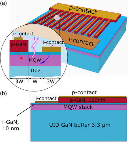
In this work, we demonstrate and study interdigitated back-contacted (IBC) GaN-based LEDs fabricated using unintentionally doped contact layers and finger-like contact geometries with different finger widths. The device structure and the interdigitated metal contacts are illustrated in Figure 1 . In such a structure, the electrical excitation of the AR is achieved by the injection of electrons directly (blue dashed lines) to the MQW region from the selective metal contact and holes (red dashes lines) from the p-GaN and both distributed in the AR by diffusion. Such structures also allow for fully scalable devices in which the AR can be extended on the whole wafer without need of etching through. In contrast to our previous devices, the bipolar carrier injection here takes place through an unintentionally doped layer, which according to our theoretical considerations solves the problem with low injection efficiencies inherent in our previous devices, where holes needed to diffuse through strongly n-type GaN. Also compared with previously reported DILED structures, the present approach fully eliminates the yellow luminescence at small excitation powers.
2 Simulations
Before presenting the experimental work, we summarize the performance expected for the structures from standard semiconductor transport equations. For this, we have carried out full device simulations of the 2D cross section illustrated in the inset of Figure 1a with different finger widths. The simulations are based on the drift-diffusion (DD) model with conventional self-consistent forms for radiative, Shockley–Read–Hall (SRH), and Auger recombination rates detailed in our previous works.[ 25 ] To make the simulations numerically less demanding while still enabling qualitative predictions, the simulation model included five QWs (typically in GaN LEDs, the bottommost QWs do not contribute much to the overall emission). Such simulations enable laying out the expected performance trends to qualitatively compare with the measured IV characteristics. In particular, they allow estimating the expected carrier diffusion through the unintentionally doped layer and the effects of changing finger widths. To summarize, the primary purpose of the simulations was to study the general characteristics of the structure as obtained from standard semiconductor device simulations, and to qualitatively compare the simulated finger width dependence with experiments. Material parameters used in the simulations were chosen based on their most established values, with the most important ones given in the following: ionized doping density 1016 cm−3 for electrons in the unintentionally doped GaN layer and 7.3 × 1018 cm−3 for holes in the p-GaN, mobility 1000 cm2/Vs for electrons and 10 cm2/Vs (in p-GaN) or 70 cm2/Vs (in i-GaN) for holes, net radiative recombination coefficient 6 × 10⁻¹⁷ m3 s−1, SRH recombination lifetime 10−7 s for both carriers, and Auger recombination coefficient 10−42 m6 s−1. The mobilities are based on our in-house measurements (for holes in p-GaN) and Ref. [30] (for electrons and holes in i-GaN). The recombination parameters represent established values frequently used in corresponding simulations.[ 31-33 ]
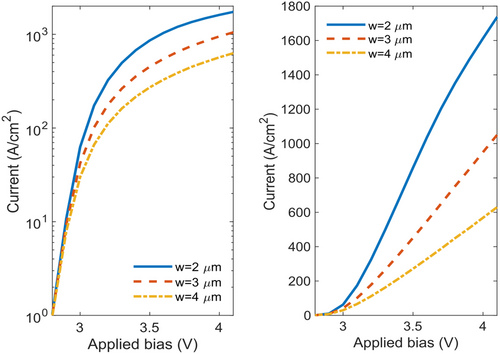
Figure 2 shows the current density as a function of applied bias with selected finger widths to present the general trends. Note that contact resistance is not included in the simulated applied biases. The current densities in Figure 2 are calculated by first integrating the simulated position-dependent current density over either contact (resulting in A/cm due to the 2D cross-section geometry, where the contact boundaries are lines), and then dividing the result by the total device width (resulting in A/cm2). All the curves represent typical LED characteristics, with the current increasing exponentially at small voltages and saturating due to internal resistance at larger voltages. The internal resistance is primarily due to the weak lateral spreading of holes due to their smaller mobility, a feature which also prompted us to use a larger width for the p-type mesa with respect to the n-type mesa in Ref.[25]. Here, using an unintentionally doped layer between the mesa areas and the MQW enables the simulated injection efficiency to be practically 1 over the simulated current range, and therefore the currents in Figure 2 are entirely due to recombination in the MQW. This happens in spite of the absence of an n-type GaN layer, as the distance for holes to diffuse to the MQW is nonetheless much shorter than the distance for them to leak to the electron contact. On the other hand, adding an n-type GaN layer in place of the electron contact would not affect the transport of electrons injected to the i-GaN, but it is expected to enable a better contact and thereby a higher overall electron injection rate in experimentally realized devices. Nevertheless, the prospect of a unity injection efficiency is a major improvement to the modeling results in Refs. [22, 23] and highlights the potential benefits from using the lateral injection configuration and unintentionally doped/intrinsic carrier transport layers when developing DDCT-based devices. The i-GaN layer thickness is an important design parameter of the structure, and here the thickness of only 10 nm enables strong diffusion of both electrons and holes to the MQW. Moreover, the simulations predict a monotonous trend between the finger widths and the attained current densities, with the smallest finger width giving the largest currents. This trend is expected to hold also for larger finger widths, in particular as the increasing distance between adjacent p-type regions hinders hole spreading over the whole device area due to the small hole mobility, thereby also limiting the amount of recombination that can be achieved at a given bias.
3 Experimental Section
The LED structures were fabricated on 2-inch c-Al2O3 sapphire substrates using metalorganic vapour-phase epitaxy (MOVPE). Devices included a 3.3 μm thick unintentionally doped (UID) GaN buffer layer, a 10 well InGaN/GaN MQW active region with QW/barrier thicknesses of 3/10 nm, a 10 nm i-GaN capping layer, followed by a 100 nm p-type GaN layer and a 20 nm p-InGaN contact layer.[ 34 ] The growth conditions are presented in Table 1 . After the MOVPE growth, the wafer was immediately transferred to an electron beam evaporation system, followed by deposition of 20 nm thick Ni and 20 nm thick Au layers on the p-GaN to form the p-type contacts in high vacuum. Then the wafer was patterned with standard lithography techniques. First, the Ni/Au layer was Ar ion milled using an ion beam etcher (IBE) to form the comb-like p-GaN metal contact, revealing the p-GaN layer outside the p-GaN metal contact. The finger-like p-GaN mesa was formed by etching away p-GaN outside the mesa using a timed inductively coupled plasma reactive ion etching (ICP-RIE) using a Cl2/Ar plasma with etching rate of 345 nm min−1. The p-type contact was formed by annealing the samples in a Jipelec JetFirst rapid thermal annealing furnace. The parameters of annealing for the p-GaN contact were the following: pump to vacuum, 1 min pumping at p = 1070 Pa (8 Torr), 5 min O2 flushing at p = 1070 Pa (8 Torr), 4 min ramp to 550 °C, 10 min at 550 °C, then free cooling under O2 atmosphere.
| Layer | Growth ambient | Temperature [°C] |
|---|---|---|
| UID GaN 3.3 μm | H2 | 1070 |
| InGaN/GaN QW 3/10 nm × 10 | N2 | 740–860 |
| i-GaN 10 nm | N2 | 860 |
| p-GaN 100 nm | H2 | 1008 |
| p-InGaN 20 nm | N2 | 1014 |
Ti/Al/Ni/Au metals as described in Ref.[35] were deposited on the i-GaN next to the p-mesa to form the i-contact for electron injection to the MQW, as shown in Figure 1a. The i-GaN contact anneal was also based on previous work[ 35 ]: pump to vacuum, 1 min pumping at p = 1070 Pa (8 Torr), 5 min N2 flushing at p = 1070 Pa (8 Torr), 4 min ramp to 760 °C, 1 min at 760 °C, then free cooling under N2 atmosphere.
For the results presented here, the length (L) of the fingers was 200 μm, and the widths (W) were 1–20 μm. The width (perpendicular to fingers) of the LED is 1000 μm, and the length of the LED (in the direction of the fingers) is 1200 μm + 2 W, so from 1204 to 1240 μm.
The electroluminescence (EL) of the fabricated back-contacted LED was measured using an integrating sphere (FOIS-1 from Ocean Optics) with the back-contacted LED inserted on the input port. The spectrum was measured using a fiber coupled spectrometer (Ocean Optics HR4000). Electrical excitation was provided by standard probes and a Keithley 2401 electrical source-meter. EL spectra were extracted through the transparent sapphire substrate or, in other words, the LED was operated in a flip-chip configuration.
4 Results and Discussion
The measured EL emission spectra of a sample with W = 2 μm are shown in Figure 3a, excited with 1–10 mA injection currents. All the spectra include a sharp peak at 439 nm with full width at half maximum (FWHM) of approximately 21 nm. The peak at 439 nm corresponds to the emission of the InGaN/GaN MQW stack, and it is the result of diffusion current injected to the active region. The In content of the QWs is estimated to be 16% by associating the EL peak at 439 nm to the composition of fully strained InGaN with bowing parameter by Orsal et al.[ 36 ] In contrast to previous work on DDCT with strongly n-doped GaN layers,[ 22, 23 ] no yellow emission is observed here at any injection current. Reasons for this can be sought by first noting that the yellow band emission is radiative electron–hole recombination through states within the GaN band gap occurring in i-GaN[ 37 ] and n-GaN.[ 38, 39 ] In the previous DDCT study[ 22, 23 ] electrons and holes had to travel through a shared 100 nm thick Si-doped n-GaN layer before reaching the MQW. In the present device, instead only a 10 nm thin GaN barrier layer is separating both the i-contact and the p-GaN from the MQW. Accordingly, we expect to see much less yellow emission already thanks to the 90% smaller volume of GaN where yellow emission can be expected. However, part of the explanation may also be better crystal quality. Note also that yellow band emission is not typically seen in InGaN QW LEDs with vertical geometries, and even the first InGaN QW LED published by Nakamura et al.[ 40 ] was free from yellow band emission. In these vertical visible blue InGaN QW LEDs, holes and electrons enter the QW(s) from different sides before at all crossing paths in GaN layers.
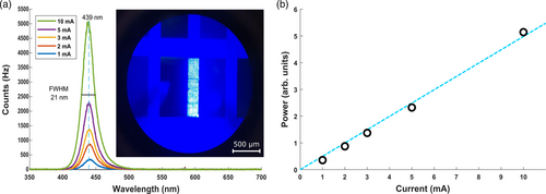
Figure 3b shows the measured total optical output power as a function of the input current (circles), and a linear fit (solid line). The LED is the same as in Figure 3, so that the EL power was extracted through the substrate side or, in other words, the LED was operated in a flip-chip configuration. The power was calculated from the spectral data in Figure 3. The data is not corrected for optical losses like the reflectivity of the integrating sphere wall or the fiber end reflection, and also the sensitivity of the spectrometer is unknown. However, the integrated EL intensity of the LED has a linear current dependence, indicating quite ideal behaviour.
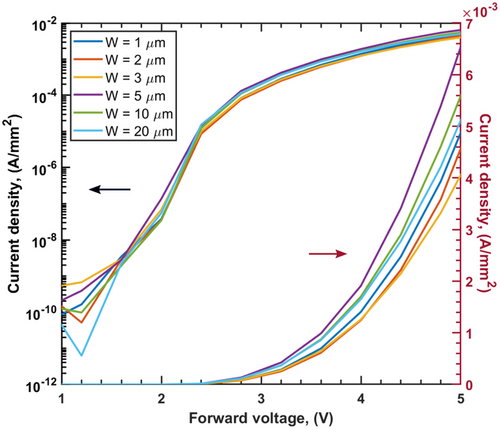
Figure 4 shows the current density–voltage (J–V) curves for back-contacted LEDs with various finger dimensions W = 1, 2, 3, 5, 10, 20 μm in linear (right axis) and logarithmic (left axis) scales. On the logarithmic scale the current density of 10−10 A mm−2 around 1 V indicates the detection threshold of the measurement device. Again, the exponential behaviour from 1.5 to 2.5 V is similar to the normal diode behaviour, and the resistive saturation afterwards resembles the series resistance which is typical for pn-diode structures. The resistance here is expected to originate partly from the internal resistivity of the device but more importantly from suboptimal thin metal contacts. Some width dependency can be observed above 3 V bias voltages on the linear scale (right), where largest currents correspond to the device with W = 5 μm. Devices with W = 5–20 μm follow the trend expected from the simulations, where increasing finger widths lead to decreasing current densities as a function of bias. Devices with W = 1–3 μm, on the other hand, do not follow this trend and exhibit smaller current densities as a function of bias than the other devices. The reason for this is a matter of speculation, but it might be due to contact resistances in the experiments varying non-monotonously between the different finger widths. Also, suboptimal contacting might lead to spotty emission patterns, which could provide another explanation for the qualitative discrepancy between experiment and theory. Therefore, in the remainder of the results, we look at the emission patterns and overall resistivities of the devices for more insight on these possible explanations.
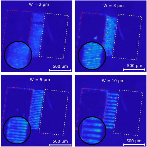
For a more visual representation of the non-monotonous finger width dependence observed in Figure 4, the EL emission colormaps of the same samples are shown in Figure 5 at a 15 mA forward current. The EL emission is spread evenly between the contact pads around the fingers in all the measured devices but there are also clear differences between the images. For the device with W = 2 μm, the emission looks intermittent and faint, which corresponds well to the high resistivity indicated in Figure 4 for this device. Some broken fingers also indicate suboptimal fabrication of such thin finger widths. The spotty emission patterns in the W = 3 μm device also indicate suboptimal contacting during fabrication. The emission is most uniformly spread between fingers in the W = 5 μm device. The inset also highlights a more even emission in the W = 5 μm device as compared to the other devices. This behaviour aligns well with the largest current densities attained for the W = 5 μm device in Figure 4. A slightly more uneven emission pattern can be seen in the W = 10 μm device as compared with the W = 5 μm device, which is in line also with the slightly smaller current densities attained for it in Figure 4.
Before concluding, we shortly investigate the origins of resistance in the structures, as the overall resistivity seems rather large in all the devices based on their measured JV characteristics. The resistivities of the semiconductor layers were estimated using the transmission line method (TLM) and test structures,[ 41 ] which were processed on the same wafer simultaneously with the LEDs. The p-layer resistivity varied between 3–7 Ω cm, while for the i-GaN capping layer the resistivity was estimated to lie between 102 and 105 Ω cm due to measurement uncertainty caused by nonideal Ohmic properties of the SC. Specific contact resistivities[ 42 ] were also estimated from the TLM, giving for the p-InGaN and as low as for some samples. For i-contact, the specific contact resistivities generally showed very high values of , but after annealing in nitrogen ambient at 720 °C, the specific contact resistivity reduced to . These values in themselves are not large enough to explain the large resistivities apparent in the JV curves. This indicates that the complete fabrication process of the proposed LEDs entails unidealities that result in worse LED contacts than what can be expected from the TLM measurements. Therefore, we expect that the samples presented in this paper could yet be significantly improved by optimizing the fabrication for both a more even emission distribution and improved i-contacts. As discussed in the Introduction, the possibility to have an unpierced MQW layer with optimized carrier spreading and no surface recombination can enable even a higher quantum efficiency than typical LEDs at high output power densities.[ 25 ] With that, the back-contacted LEDs with unintentionally doped carrier transport layers proposed in this work offer an interesting alternative for diffusion-driven back-contacted large-area LEDs with unity injection efficiency and no need for lateral doping.
5 Conclusion
In conclusion, this work provided the experimental demonstration that back-contacted diffusion-driven GaN LEDs could be fabricated without typical lateral doping techniques and n-doped GaN layers, potentially leading to unity injection efficiencies according to device simulations. Combining selective interdigitated back-contacts and the DDCT concept, the samples demonstrated sharp blue emission at 439 nm with excitation currents from 1 to 10 mA without the parasitic yellow emission observed in previous works on diffusion-driven GaN LEDs. Comparing the results from simulations and experiments with different contact geometries indicated that the contacting and fabrication process was still suboptimal especially at the smallest contact and mesa sizes. However, according to TLM measurements carried out on bulk samples in this work, major improvements in the contact resistance are possible also for the i-type GaN. With decreased contact resistances, the back-contacted LEDs utilizing direct QW injection and diffusion-driven lateral current transport might enable extremely large area III–V light emitters or other large area III–V devices for the GaN based material systems.
Acknowledgements
The authors acknowledge financial support from the Academy of Finland Flagship Programme, Photonics Research and Innovation (PREIN), decision number: 320167 and the Academy of Finland (Grant No. 315403). Computational resources provided by the Aalto Science-IT project were used to carry out the simulations of this article. The samples fabrication was performed at the OtaNano—Micronova Nanofabrication Centre of Aalto University.
Conflict of Interest
The authors declare no conflict of interest.
Open Research
Data Availability Statement
The data that support the findings of this study are available from the corresponding author upon reasonable request.


