Aberration Corrected Analytical Scanning and Transmission Electron Microscope for High-Resolution Imaging and Analysis for Multi-User Facilities
Abstract
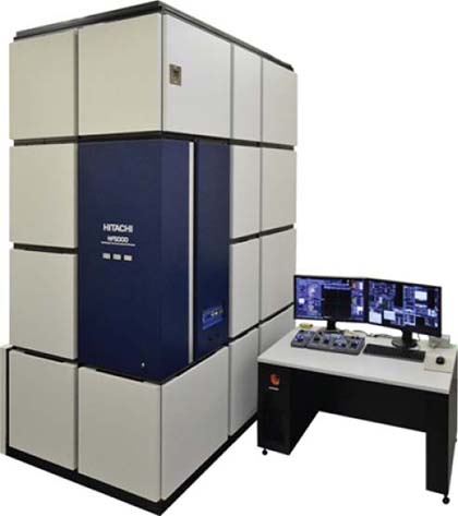
In recent years the revolution in aberration correction technology has made ultrahigh resolution imaging and analysis routinely accessible on transmission electron microscope (TEM) and scanning transmission electron microscope (STEM). We have developed a new analytical 200 kV cold field emission TEM equipped with a probe-forming aberration corrector, the model is Hitachi HF5000 (Figure 1). The microscope is fully covered in a metal enclosure to reduce the influence from environmental acoustic noise and temperature variation. Remote operation through Ethernet communication is possible as a result of a new design individual microprocessor circuit. Regarding the atomically resolved analytical capability, one of the key demands is to achieve high performance at a multi-user facility. To meet this demand, the Hitachi HF5000 is designed to be user friendly and extensive sample capability covers most requirement s from users in the fields of material science, materials fabrication, and device industry.
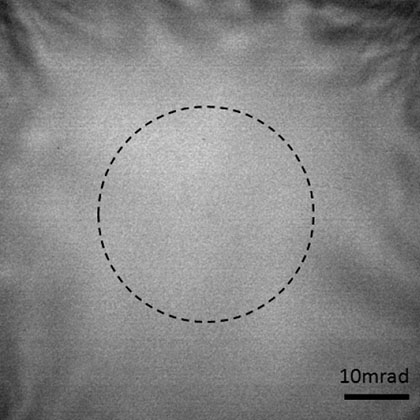
The HF5000 is capable of TEM imaging, STEM imaging with bright field (BF), annular dark field (DF) detectors, and secondary electron (SE) imaging. The probe-forming aberration corrector with automated correction of up to third order aberrations allows users to obtain aberration-free STEM illumination optics with minimized effort. Figure 2 gives an example after the aberration correction, the Ronchigram pattern of the amorphous specimen shows an approximately 32 mrad half angle flat region, corresponding to the optimal aperture condition for aberration-free STEM imaging. While TEM and STEM imaging probe the bulk structure of specimens, the SE imaging helps understanding the surface structure. It is important to note that the SE image can be acquired simultaneously with STEM image therefore both surface and bulk structures are revealed side-by-side at the same time, even at atomic resolution [1]. Such a triple imaging capability on one microscope column is very unique and critical in studying heterogeneous materials such as catalysts.
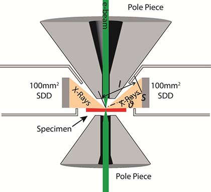
For modern analytical TEM, the most desirable features are high spatial resolution, high signal detection sensitivity, and sufficient specimen tilting angle range. New pole-piece is therefore designed for HF5000 which enables sub-angstrom resolution DF-STEM imaging and a large specimen tilt angle of +/−35 degrees. Figure 3 shows a high-angle annular DF (HAADF)-STEM image of a silicon thin film at the zone-axis direction, Si dumbbells with a 78 pm separation between adjacent Si columns are resolved. To make X-ray analysis highly sensitive, increasing solid angle of the Energy Dispersive X-ray spectroscopy (EDX) detector is essential. Two 100 mm2 silicon drift detectors (SDDs) are installed on the HF5000, the distance between detector and specimen (l) is carefully managed to maximize the solid angle. In order to increase peak to background ratio (P/B), the SDDs are positioned as high as possible relative to specimen surface. The large take-off angle (q) reduces X-ray absorption and continuum X-rays which radiates with an angular intensity distribution. The improvement of resolving power is also related to the increased long term stability. High voltage circuits are carefully designed, and stability for power supply of lens and deflection coils is enhanced. A stability of 0.6 ppm/min for circuit current is achieved for one of the beam deflection coils. In addition, the stability for the newly designed high tension circuit is less than 1 ppm which is critical to realize high energy resolution for analytical work using cold field emission gun and high spatial resolution for imaging.
Figures


