Digital Shear Printing of Mechanically Robust Liquid Metal Circuits with Hierarchical Embedded Structure for Paper Electronics
Abstract
The seamless integration of recyclable and deformable liquid metal (LM) conductors into paper is attractive to developing flexible, breathable, and green electronics. However, the weak adhesion between paper and LM complicates the patterning. In addition, the low damage endurance of LM, an open problem for on-surface conductors, restricts the practical applications. Here, a simple yet efficient approach of shear printing is reported to directly pattern hierarchical embedded LM circuits with erasure resistance onto paper. This is achieved by digitally applying the shear force to the solid gallium film to induce its adhesive wear with the paper, allowing the gallium to be embedded into the paper's fiber networks. Meanwhile, the pressure-induced formation of microgrooves on paper allows the LM circuits to be surface-embedded onto paper. The hierarchical embedded structure endows the LM circuits with enhanced mechanical damage endurance that they can even withstand eraser rubbing and tape peeling. Applications of the hierarchical embedded, mechanically robust, and breathable LM-enabled paper electronics in enhanced humidity sensing, electrophysiology monitoring, and digital droplet microfluidics are also shown. This work opens doors to developing sustainable yet robust paper electronics by rationally utilizing the solid properties of low-melting-point metals.
1 Introduction
The information age is characterized by the mass production of electronic devices that merge with and shape human life while posing a significant environmental issue of electronic waste.[1] Therefore, there is an urgent need to produce sustainable electronic devices with recyclable conductors and degradable substrates.[2, 3] In this context, paper, a ubiquitous, degradable, and bio-based material in our daily life, has emerged as an attractive film substrate for green electronics due to its abundance, low cost, and eco-friendliness.[4-6] Moreover, paper possesses additional desirable properties such as flexibility, lightweight, breathability, capillarity, and foldability.[7] These features have been effectively utilized in creating functional electronics for applications ranging from wearables[8] to disposable diagnostic tools.[8, 9] Among various conductors, metals with high electric/thermal conductivity offer many opportunities for creating high-performance paper electronics, such as wearable and breathable sensors,[10] highly sensitive electrochemical and optical sensors,[11] and energy-related applications.[12] However, current methods for depositing solid metals on paper are unsustainable. For example, electronic beam evaporation and sputter deposition require expensive equipment with high-energy demand,[12] making fabrication challenging in resource-limited settings. Alternatively, methods of chemical reduction of metal precursors and depositing metal nanoparticles necessitate complex material synthesis, expensive precursors, post-sintering, and the use of environmentally unfriendly chemicals.[13-15] Thus, a cost-effective and sustainable metal deposition approach is highly required for green paper electronics.
Gallium-based liquid metals (LMs) that can be deposited on paper in a solvent-free manner, have emerged as a promising option for green processing of paper electronics.[16-19] The liquid nature of these metals also enables the development of highly deformable paper electrodes with stable conductivity.[20] Moreover, LMs offer additional advantages such as high conductivity, solid–liquid transition, ease of recycling, non-toxicity, and high reflectivity,[21-25] which could expand the potential applications of paper electronics in intelligent systems and biomedicine.[26, 27] The prerequisite for these applications is to enhance the adhesion between the LM and paper. This is because the rough and chemically inert paper surface is supermetallophobic and repellent to LMs with high surface tension. To address this challenge, many efforts have been dedicated to increasing the interfacial adhesion through the surface engineering of paper or LM, such as surface modification of paper using adhesives,[28] enhancing the oxidation of LM,[16] and force-induced wetting.[19] Alternatively, printing LM microdroplets on paper can avoid the adhesion issue, but the post-mechanical sintering step is required to recover the conductivity.[29] In addition to complicated fabrication processes, existing methods can only deposit LM on paper surfaces. This makes LM prone to mechanical damage in practical applications, which is also an open problem for all on-surface conductors.[18, 30] Thus, it is attractive to develop a simple, pretreatment-free manner to pattern mechanically robust LM circuits on paper. However, concurrently addressing the critical issues of low interfacial adhesion and poor durability of LM in a single printing step remains a great challenge.
Pencil writing, a revolutionary technique involving the wear of soft graphite onto paper by shear force, was developed centuries ago and remains in use today.[31] Inspired by pencil writing, we show that soft solid gallium circuits can also be directly printed on paper under shear force. The shear force can induce the wear of gallium film to allow its transfer and embedding into the fiber networks of the paper. Thus, the adhesion between the paper and the LM can be enhanced without requiring any surface modification of the paper. Additionally, we observed that the mechanical pressure induced the formation of microgrooves on the paper due to its plasticity, and the LM can be surface-embedded on paper. The shear-printed LM circuits with hierarchical embedded structure can endure tape-peeling, and even rubbing with an eraser. We also found the embedded LM circuit is sensitive to humidity. Other applications such as electrophysiology monitoring and digital droplet microfluidics were also demonstrated.
2 Results and Discussion
2.1 Direct Shear Printing of Hierarchical Embedded LM on Paper
Like aluminum, solid gallium is also soft but differentiated by its low wear resistance. Essentially speaking, printing is a process of controllably transferring materials to substrates. Here, we aimed to utilize the wear-induced material transfer to achieve direct printing of gallium on paper. A classic wear-induced transfer printing can be seen in writing with a pencil, in which the graphite was worn and deposited on paper under shear force.[8] In a typical printing operation, we covered the paper with a thin and solid gallium film (30 μm in thickness, Figure S1, Supporting Information), followed by using a low-cost (30$) computer-controlled pen-plotter to digitally apply the shear force to the film in a rapid (2000 mm min−1) and on-demand way (Figure1a and Figure S2, Supporting Information). A ball-point pen with a ball diameter of 500 μm was used for the exertion of the shear force (Figure S3, Supporting Information), and its movement and contact with the gallium film can be precisely controlled by the stepper motors of the plotter. To avoid mechanical distortion of gallium film and underlying paper during shear printing, a thin polyethylene terephthalate (PET) film as a protective layer was attached to the gallium film (Figure S4, Supporting Information). More details of the printing setup and operation were provided in the Experimental and Movie S1, Supporting Information.
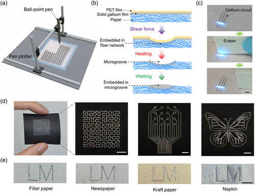
Under the high applied pressure of ≈100 MPa, the soft gallium and paper experienced plastic deformation and close contact with each other. The shear force then induced the wear of gallium accompanied by its transfer and embedding into the fiber network of the paper, as discussed later. Along the process, the compression of the paper with plasticity leads to the formation of microgrooves on the paper. Thus, the worn gallium was conformally adhered to the microgroove's surface. After applying shear force, the gallium film was melted to turn the circuits to the liquid state and also facilitate the removal of gallium residue. We observed the dewetting-induced shrinkage of the film due to the high surface tension of liquid gallium.[32] After peeling off the PET film, we used a paper sheet to rub away excess liquid gallium. In this process, the liquid gallium tends to fill into the microgrooves of the paper since the worn gallium can be taken as metallophilic coatings. Finally, the LM circuits were surface-embedded into the microgrooves of the paper, as shown in Figure 1b and Movie S2, Supporting Information.
Our hierarchical embedded structure design concurrently addressed two critical challenges faced by LM-based paper electronics: low interfacial adhesion and poor mechanical durability of liquid circuits. In our method, since the gallium was forced into the paper in its solid state, the issue of low interfacial adhesion between paper and LM can be fundamentally avoided. Thus, our method did not require any surface modification of the paper, which is frequently involved in conventional patterning methods.[20, 28] Moreover, benefiting from the hierarchical embedded structure, the printed LM circuits show enhanced mechanical damage endurance that they can even withstand eraser rubbing (Figure 1c). This allowed to creation of robust LM electrodes on paper to electrically interface with other objects for interconnection, sensing, or stimulation. Note that this surface-embedded structure with circuit protection ability was synchronously formed along the application of shear force, without pre- or post-treatment of the paper.
Based on the digital shear-printing method, complex LM patterns with microscale line width of ≈300 μm can be obtained in a simple, low-cost, rapid, and green manner (Figure 1d). This indicates its potential for on-demand fabrication of various paper-based microelectronic device. Our method is also compatible with different kinds of paper. Figure 1e shows the word “LM” was shear-printed onto various paper substrates, such as filter paper, newspaper, and napkin (Figure S5, Supporting Information). The good substrate compatibility of the printing method may inspire the design of devices with different functional paper substrates for wide applications. Note that the gallium has the supercooling effect, and thus the circuit can maintain the liquid state below the gallium's melting point of 29.8 °C.[33, 34]
2.2 Mechanism of Shear Printing
To clearly illustrate the printing process, we used electron and laser scanning microscope to capture the morphology change of the gallium film and paper for each step: applying shear force, heating, and wetting, as shown in Figure 2a and Figure S6, Supporting Information. Initially, a smooth solid gallium film of low surface roughness (Sa = 0.3 μm) and thickness of 30 μm was covered on the paper (Figure 2a,i). After applying the shear force at a load of 6 N and three cycles, the pen point dented the thin gallium film (Figure 2a,ii). After heating, a microgroove with a depth of 20 μm was observed on the paper and a layer of gallium was embedded to the fiber networks of the microgroove surface (Figure 2a,iii). When we scraped the residual liquid gallium on the paper, the liquid gallium wetted and filled the microgroove, resulting in a surface-embedded liquid gallium line with a width of 340 μm and height of 40 μm above the paper surface, as shown in Figure 2a,iv.
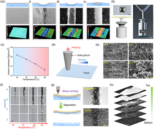
The key step of this printing process is the shear force-induced selective embedding of gallium to the paper (Figure 2a,iii). To uncover its underlying mechanism, we performed the wear analysis. The wear mode between the soft gallium and paper can be considered as adhesive wear, which is characterized by the material transfer from one contacting surface to another by a cold-welding process during the relative motion.[35] We did observe the solid gallium film was welded to the paper surface after applying the shear force. To intuitively show wear-induced cold welding, we printed a gallium sheet (5 * 5 mm) onto the paper and maintained the sheet in a solid state. The gallium sheet can withstand the pull of a 100 g weight (Figure 2b), with a pull-off adhesion strength of 0.1 MPa.
We then captured the transfer of the gallium lines to the paper at different loads (2, 4, 6, 8 N) and temperatures (10, 15, 20, 25 °C). As shown in Figure 2f and Figure S7, Supporting Information, the wear and transfer of the gallium are restricted at low loadings or low temperatures so that the gallium cannot be embedded in the paper. High temperatures and high loadings did increase the wear volume, resulting in the highly efficient transfer and adhesion of gallium to the paper. These results coincided with Holm–Archard's model and provided important guidelines for designing the printing parameters. This also explains why we cannot fully reproduce the printing results when transiting from summer to winter in our initial attempt of the work.
Other factors that may affect the printing performance such as the gallium film thickness, printing speed, and printing cycles, were also investigated at load of 4 N and temperature of 25 °C. When a thicker gallium film was used, the wear-induced transfer of the gallium was hindered due to the increased stress dispersion, as shown in Figure S8, Supporting Information. Consequently, the gallium lines became thinner and uneven when the thickness of the gallium film increased. The gallium lines could not be formed at the thickness of 240 μm. Similarly, the thicker protective PET film also hindered the transfer of gallium to the paper by dispersing the stress (Figure S9, Supporting Information). Since the fabrication of thinner and intact gallium film was challenging by press casting, we used the gallium films with a thickness of 30 μm for subsequent printing operations.
We found that when a low printing speed of less than 30 mm min−1 was applied, the gallium lines could not be printed on the paper (Figure S10, Supporting Information). This is because, at low printing speed, the pen equivalently applies static pressure to the gallium film instead of the shear force. Thus, the shear-induced adhesive wear was limited. Additionally, increasing the printing cycles can enhance the wear and transfer of the gallium, and the gallium tends to penetrate to the backside of the paper (Figure S11, Supporting Information). This provides an opportunity to create double-sided electrical interconnection (Figure S12, Supporting Information), which plays an important role in creating multilayer printed circuit boards.[38] Moreover, the line width can be controlled by changing the load, printing cycles, and the diameter of the ball of the pen (Figure S13, S14, Supporting Information). In an optimal pattern of parallel lines, the minimum line width of 230 μm and line distance of 140 μm were demonstrated (Figure S15, Supporting Information).
To understand the wear at the microscale, we peeled off the solid film from the paper after applying the shear force. The scanning electron microscopy (SEM) images show the paper fibers were detached from the paper substrate and compacted to the gallium film, as shown in Figure 2g. This result further indicated that the gallium was cold-welded into the paper fibers under the shear force. The SEM and energy-dispersive X-ray mapping characterization further confirmed that the paper contacting the gallium line was compressed, and the gallium was embedded in the microgrooves (Figure S16, Supporting Information). The microcomputed tomography characterization shows the hierarchical embedding of gallium along the thickness direction, as shown in Figure 2h and S17, and Movie S3, Supporting Information. Close to the bottom of the paper, the wear debris of gallium with embedding to the paper fiber network was observed. The gallium debris acted as metallophilic anchors to attract the liquid gallium to be surface-embedded into the microgrooves. Thus, a continuous and uniform gallium line can be observed in the microgrooves of the paper.
We also tried to print other metals such as aluminum, tin, and zinc, which are soft and exhibited relatively poor wear resistance at ambient conditions. However, all the metals with higher wear resistance than that of the gallium, cannot be welded and thus printed to paper (Figure S18, Supporting Information). This also highlighted the importance of the low wear resistance of gallium, which provides a unique opportunity for direct printing of LM on paper by shear force. The low wear resistance of gallium could be attributed to the weak interatomic bonding of the solid gallium.[39] Gallium is rather unique among other metals in that it has both covalent and metallic bonding composed of dimers.[40] The large distance between the gallium dimers leads to weak binding and thus the low cohesive energy of the solid gallium. From a fundamental perspective, adhesive wear is inherently linked to the cohesive strength of the gallium and the adhesive strength of the interface. Therefore, the solid gallium with low cohesive strength tends to detach and transfer to other surfaces during friction.
2.3 Characterization of Hierarchical Embedded LM Circuits
Next, we performed the systematical characterization of the hierarchical embedded LM circuits highlighting their electromechanical stability, breathability, recyclability, and biocompatibility. Firstly, the liquid nature endowed the circuits with intrinsic flexibility, allowing the paper electronics to maintain functionality under large deformation. In a folding test, the circuit kept its electric connection even when the paper experienced a large deformation of a 180° fold. In contrast, cracks were observed in the solid gallium, leading to the electrical failure (Figure 3a). Cyclic folding at 180° tests showed the liquid gallium circuit exhibited minimal resistance change (<1%) after 1000 cycles (Figure 3b), indicating its excellent mechanical stability.
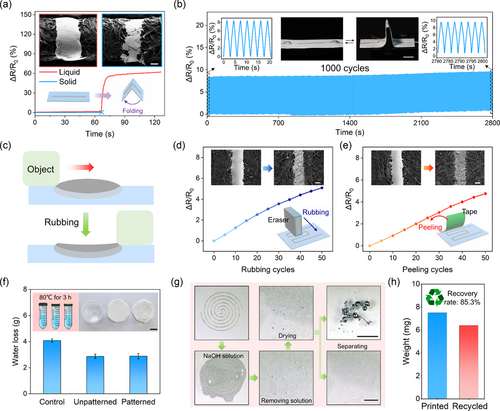
Unlike conventional patterning methods that deposit LM on the paper surface, our method allowed the circuits to be embedded into the porous microfibers and microgrooves of the paper. Thus, when rubbing with paper, the LM beneath the paper surface would not be wiped away (Figure 3c). To investigate the mechanical damage endurance of the liquid circuits, we conducted mechanical rubbing and peeling tests. In the rubbing test, we used an eraser to rub the LM circuit with a pressure of 1.5 kPa. After 50 rubbing cycles, the circuit maintained its conductivity and its resistance increased from 2.2 to 13.5 Ω (Figure 3d). In the tape-peeling test, we used tape to peel the LM circuit with a 1.94 N m−1 peel strength. After 50 peeling cycles, its resistance increased from 2.4 to 13.8 Ω (Figure 3e). In contrast, for on-surface LM circuits, the circuit's connection was permanently damaged after only one rubbing or peeling cycle (Figure S19, Supporting Information). Moreover, the good resistibility to tape-peeling of the printed LM circuits allows us to remove LM residuals by the tape without destroying the circuits (Figure S20, Supporting Information).
The porous nature of the paper endowed paper electronics with permeability or breathability, which is desirable in applications such as wearable and bioelectronic devices that require conformable attachment.[41] Here, we compared the breathability of the paper printed with and without the gallium circuit (9.7% area ratio) by using them to seal the centrifuge tubes. In the oven at 80 °C for 3 h, the tub sealed by the paper with the LM circuit lost a similar amount of water (2.88 ± 0.21 g) as the one without the circuit (2.86 ± 0.16 g), as shown in Figure 3f, indicating that the printed circuit had little effect on the intrinsic breathability of the paper.
To investigate the biocompatibility, we cocultured the NIH 3T3 cells with the gallium for three days. As a result, the cytoactivity of the cells was almost the same as that of the control group in the three days (Figure S21, Supporting Information), indicating the good biocompatibility of the gallium. Moreover, the skin showed no adverse reaction even after wearing the LM circuits for 8 h due to the good permeability of paper and biocompatibility of the LM (Figure S22, Supporting Information). These results encouraged us to explore the potential applications of the printed LM circuits in epidermal electrodes and human–machine interaction, as discussed later.
Recovery of metals is essential to resource conservation and environmental protection. However, traditional high-melting metal recovery typically involves high-temperature processes such as smelting, leading to high energy consumption.[42] The room-temperature LMs have unique physical and chemical properties such as the adjustable surface tension, allowing a low-energy but high-efficiency recovery method using acidic/basic treatment.[43, 44] To recycle the liquid gallium, we used 0.1 m sodium hydroxide solution to treat the paper. The solution can remove the gallium oxide on the gallium surface to increase the surface tension of the liquid gallium. Thus, the liquid gallium circuit was broken and extruded from fibers to the paper surface and fused into multiple particles. After solidifying the gallium microparticles, we can easily collect them by shaking or brushing them off, as shown in Figure 3g. The recovery rate of gallium can reach 85.3% (Figure 3h), and the recovered gallium can be directly reused for the fabrication of gallium film without purification. It's also noted that the printed LM circuit exhibited a minimal quantity of ≈0.35 mg cm−1 with a line width of ≈300 μm, indicating our approach helps reduce overall consumption and can make it more feasible for use in low-cost or even disposable devices.
2.4 Hierarchical Embedded LM Circuits for Paper-Based Humidity Sensor
Next, we aimed to explore the potential applications of LM-enabled paper electronics. We unintentionally found the LM printed on filter paper exhibited a unique humidity-sensing ability. This can be attributed to the strong hydrophilicity of the filter paper made by the network of cellulose fibers, which have abundant hydroxyl groups.[45, 46] When the ambient humidity increases, the cellulose fibers absorb the water and swell. The swollen cellulose fibers separate the embedded gallium microparticles and reduce the conductive paths, leading to an increase in the resistance (Figure 4a). Compared with the on-surface gallium circuit fabricated by a magnetic printing method,[17] the shear-printed circuit exhibited enhanced sensitivity in humidity sensing (Figure 4b). At the same relative humidity (RH) change from 11% to 97%, the relative resistance change (1.68%) of the embedded gallium circuit was seven times that (0.24%) of the on-surface, as shown in Figure 4c. In addition, the resistance of the embedded gallium circuit increased linearly (R2 = 0.998) with the RH ranging from 11% to 97%, and the humidity sensitivity was about 0.015. Moreover, the resistance of the embedded gallium circuit exhibited stable change during 500 humidity change cycles, indicating its good repeatability (Figure S23, Supporting Information).
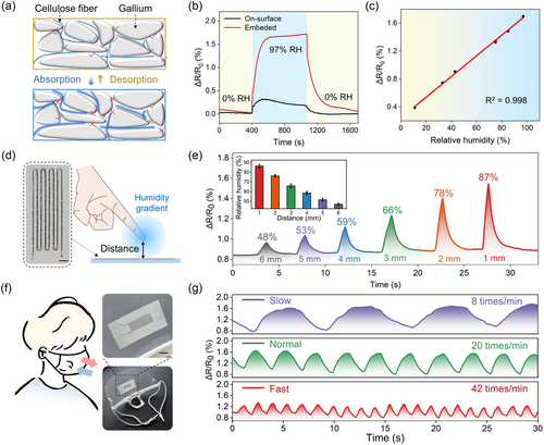
The gradient humidity field near the human skin provides a unique opportunity for non-contact human–machine interaction based on the humidity sensor (Figure 4d). As a “proof-of-concept” demonstration, we created a snake-like embedded gallium circuit as the interactive humidity sensor. Figure 4e shows the sensor can distinguish the motions of the approaching and moving away of the index finger based on the skin humidity-induced resistance change with a high spatial distance resolution of 1 mm. Considering that the resistance change of the gallium circuit may be caused by the heat radiation from the finger, we wrapped the finger with a piece of aluminum foil to isolate the humidity. The resistance change induced by the wrapped finger was much less than that induced by the bare finger, indicating the sensor resistance much depended on the humidity (Figure S24, Supporting Information).
In addition to non-contact human–machine interaction, the paper-based humidity sensor can also monitor the respiratory rate and pattern for health management by integrating the sensor with a commercial mask (Figure 4f). As breathing out, the exhaled air contains abundant water, and its RH approaches 100%, which increases the resistance of the sensor. When breathing in, the surrounding atmosphere with lower RH than the exhaled air leads to a decrease in the water in the cellulose microfibers and thus the resistance. Based on this mechanism, the paper-based humidity sensor can monitor respiratory patterns at different rates of 8, 20, and 42 times/min (Figure 4g), which can meet the needs of daily and clinical respiratory monitoring.
2.5 Hierarchical Embedded LM Circuits for Interactive and Sensing Interfaces
In addition to non-contact applications, the unencapsulated and anti-erasure LM circuit provided a unique opportunity to create a robust electric interaction interface for applications such as tactile and electrophysiological sensing. For comparison, we created on-surface and surface-embedded spiral LM circuits by magnetic printing[17] and shear printing, respectively. In a rubbing test, we attached the LM circuits to the skin and rubbed it with a pressure of ≈5 kPa (Figure 5a,i). Since the on-surface LM circuit was very vulnerable to mechanical damage due to its fluidity, it was smeared out after the rub test (Figure 5a,ii). However, the surface-embedded circuit maintained its integrity after rubbing (Figure 5a,iii), indicating its potential applications in creating robust electrode–tissue interfaces for sensing or stimulation.
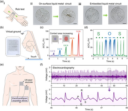
To demonstrate its potential applications, we created an interdigitated LM electrode by shear printing to serve as a capacitive sensor for tactile sensing. As the finger touches the interdigitated electrode, it is equivalent to connecting another capacitor in parallel,[47, 48] leading to an increase in the capacitance, as shown in Figure 5b. With removing the finger, the capacitance can recover to its initial value. It noted that the touch sensor exhibited a short response time of 57 ms and recovery time of 61 ms, and good repeatability during 1000 touch cycles (Figure S25, S26, Supporting Information). In addition, when the pressure increased from 0.2 to 1.0 N, the contact area between the finger and interdigitated electrode increased. Meanwhile, the relative capacitance change increased from 18% to 143% (Figure 5c), showing excellent tactile sensitivity. Moreover, we can input dot or dash signals of Morse Code by keeping in touch for a short and long time, respectively, for electrocommunication. For example, when it needs to send the international distress signal “SOS”, the corresponding Morse code is “···---···”, as shown in Figure 5d.
We also printed a Peano circuit of a 10% area ratio on the paper as an epidermal electrode. By attaching two LM electrodes to the chest (Figure 5e), a continuous electrocardiograph signal was obtained (Figure 5f). The PQRST peaks can be distinguished in the obtained ECG signals. Meanwhile, a low-pass filter was used to separate the noise and effective signal parts to calculate the signal-to-noise ratio (SNR). As a result, the SNR of the ECG signal acquired by the LM electrodes was 16.1 dB, close to 17.1 dB of the commercial Ag/AgCl gel electrode (Figure S27, Supporting Information). More importantly, compared with the Ag/AgCl electrodes, the LM electrodes exhibit excellent breathability, enhancing comfort by allowing air circulation, reducing heat buildup, and preventing moisture accumulation. After attaching the Ag/AgCl and LM electrodes to a mouse skin for 72 h, there was obvious inflammation and tissue damage in the group of the Ag/AgCl gel electrode but not in the group of the LM electrode through optical images and H&E histopathological analysis (Figure S28, Supporting Information). This suggests the LM electrodes have the potential to serve as a comfortable and user-friendly human–machine interface.
2.6 Hierarchical Embedded LM Circuits for Paper-Based Microfluidics
To demonstrate the potential applications of the simple and low-cost printing method in analytical devices, we create a digital microfluidic device by using the hierarchical embedded LM electrodes for active droplet manipulation on paper. Digital microfluidics is an emerging lab-on-a-chip technology that can manipulate droplets on a patterned array of electrodes based on the electrowetting-on-dielectric (EWOD) phenomenon.[49, 50] EWOD allows the precise control of droplet wettability and movement of a liquid droplet on a dielectric surface by modifying the applied electric field.[51] However, conventional electrodes designed for EWOD devices involved tedious and high-cost fabrication techniques such as photolithography.[52] Here, we designed the paper-based EWOD device composed of an LM electrode array layer and a polyethylene dielectric layer, as shown in Figure 6a. The electrode layer was fabricated by shear printing of one grounding electrode and eight working electrodes on the paper, as shown in Figure 6b. It's noted that the end of the grounding and working is designed as the planar electrodes serving as the contact pads, which were fabricated by increasing the line density (Figure S29, Supporting Information). When an electric field is applied on one working electrode, the contact angle of the droplet and PE layer is reduced and the droplet tends to move to the activated working electrode, as shown in Figure 6c. Thus, the droplet can be manipulated by sequential activation of the working electrodes, as shown in Figure 6d and Movie S4, Supporting Information.
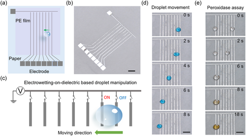
We then used this device to manipulate the droplet for the colorimetric detection of peroxidase, which is widely existing in organisms and can catalyze hydrogen peroxide. Initially, the droplets of peroxidase solution and detection solution were located at the two ends of the electrowetting device, as shown in Figure 6e and Movie S5, Supporting Information. By activating the working electrodes, the detection droplet was driven to approach the peroxidase droplet. Once the droplets contacted each other, they merged into a larger droplet. In the presence of hydrogen peroxide, peroxidase can oxidize guaiacol to produce a brown substance. As a result, the mixed droplet turned from transparent to brown within 10 seconds. Here, we only demonstrated a typical application for biosensing, and our shear-printed LM electrodes may find wide applications in low-cost analytical devices for point-of-care testing, such as flexible electrochemical sensors, electrokinetic sample pretreatment, and electrothermal microfluidic devices for molecular diagnosis.[53, 54]
3 Conclusion
In summary, we reported a simple yet efficient way to pattern hierarchical embedded LM on paper by shear force. We experimentally showed that the underlying printing mechanism is the wear-induced material transfer benefiting the low-wear resistance of solid gallium. This method not only overcomes the low interfacial adhesion between paper and LM but also allows the formation of grooved microstructures on paper for circuit protection. We also showed the shear-printed LM circuits have advantages in terms of enhanced mechanical damage endurance, breathability, deformability, and good biocompatibility. We also demonstrated the facile creation of functional paper electronics in enhanced humidity sensing, permeable wearable electrophysiology sensing, and low-cost droplet microfluidics. This work opens doors for developing new patterning methodologies and sustainable electronics by rationally using the unique properties of low melting point metals in their solid state. Future research should focus on the numerical modeling of such a unique wear process.
4 Experimental Section
Materials
Pure gallium (Ga, 99.99%, melting point: 29.8 °C) was obtained from Dongguan HuaTai Metal Material Technology Co., Ltd., China. Gallium should be stored in a plastic container and avoided contact with other metals during usage to prevent the metal corrosion and contamination. The thickness of the A4 printing paper is ≈100 μm (No. 7362, Deli), and the mercury intrusion porosimetry test showed the paper has an average pore diameter of 1.8 μm with a porosity of 42%. Other paper substrates such as filter paper and Kraft paper were purchased from the local market (Nanjing, China).
Characterization
The resistance was measured using the digital multimeter (DMM 6500, Keithley). The scanning electron microscopy (SEM) observations were performed using an UltraPlus Zeiss microscope system. The micro-computed tomography (Micro-CT) was obtained by using a three-dimensional X-ray microscope (Zeiss Xradia 510 Versa). The hardness of the gallium was measured using Vickers Hardness Tester (VH-5LDC) with a load of 300 gf and a dwell time of 10 s. The profile of the LM circuit and paper was measured using a 3D laser scanning microscope (VK-X1000).
Fabrication of Solid Gallium Films
The solid gallium films were fabricated by press casting. In a typical operation, a liquid gallium droplet (0.2 mL) was sandwiched with two polyethylene terephthalate (PET) films, between which a double-sided tape with a thickness of 30 μm was used as the spacer. Then, the liquid gallium droplet was compressed into a liquid film. To solidify the liquid film, we used a solid gallium bead to contact the film to trigger the nucleation at room temperature. The thickness of the obtained solid gallium films ranged from 30 to 240 μm by varying the spacer thickness.
Shear Printing of LM Circuits on Paper
A commercial full-automatic pen plotter (Guangku) was used for digitally applying the shear force. In a typical operation, we covered the paper with a solid gallium film. Then, a PET film with a thickness of 25 μm was covered on the solid gallium film. The shear printing was typically repeated three times. After that, we heated the gallium film using a hot gun or hotplate. Finally, we removed the PET film and scraped the residual LM using a paper sheet. The load of the printing can be adjusted by changing the initial distance between the pen point and paper, and the load force was detected using a force sensor (HZC-TD3-10 N, Chengying). For experiments involving printing mechanism studies (Figure 2), we added weights to the pen to adjust the load. The temperature was measured and controlled using a thermocouple thermometer (KPS-02, Kaipusen) and a Peltier Cooler (Yuliang Electronics).
Electrocardiogram Signal Acquisition
Two LM electrodes were affixed to the chest for bipolar leads of the electrocardiogram. The electrocardiogram acquisition device was mainly composed of a microprogrammed control unit (nRF52840, Nordic Semiconductor) and an analog-to-digital converter (ADS1299, Texas Instruments). The obtained data were processed using a 50 Hz notch for removal of power frequency interference and wavelet basis function (db4) with decomposition level 5 for denoising. All experiments were conducted in strict compliance with the rules and with the approval of the Ethical Committee of Southeast University. Informed consent was obtained from the volunteers for all the experiments involving human participants.
Droplet Manipulation Based on Electrowetting
The driving voltage was applied by a high-voltage power supply (H2-A, Dongwen). The colorimetric detection of peroxidase was achieved by using the Micro Peroxidase Assay Kit (Solarbio).
Acknowledgements
We thank the Analysis and Testing Center of Southeast University for providing the scanning electron microscope, and hardness test. This work was supported by the Natural Science Foundation of Jiangsu Province (grant no. BK20220859), the China Postdoctoral Science Foundation (grant no. 2022M710667), the Open Research Fund of the State Key Laboratory of Digital Medical Engineering (grant no. 2024K02), SEU Innovation Capability Enhancement Plan for Doctoral Students (grant no. CXJH_SEU 24144), and Postgraduate Research & Practice Innovation Program of Jiangsu Province (grant no. KYCX24_0473).
Conflict of Interest
The authors declare no conflict of interest.
Author Contributions
Biao Ma: data curation (lead); funding acquisition (equal); investigation (lead); methodology (lead); writing—original draft (lead). Gangsheng Chen: data curation (lead); funding acquisition (supporting); investigation (lead); methodology (lead); writing—original draft (lead). Yi Chen: data curation (equal); investigation (equal). Jin Zhang: methodology (equal). Yanjie Chen: investigation (supporting). Haoran Deng: writing—review and editing (supporting). Yakun Gao: data curation (supporting). Mengwen Yan: data curation (supporting). Jingtai Shang: methodology (supporting). Heng Zhang: data curation (supporting). Feng Zhang: methodology (supporting). Chang Cui: investigation (supporting). Chao Zhao: writing—review and editing (supporting). Hong Liu: funding acquisition (lead); supervision (lead); writing—review and editing (lead). Biao Ma and Gangsheng Chen contributed equally to this work.
Open Research
Data Availability Statement
The data that support the findings of this study are available from the corresponding author upon reasonable request.


