Benchmarking Inorganic Thin-Film Photovoltaics Technologies for Indoor Applications
Abstract
The growing demand for sustainable power solutions for Internet of Things (IoT) systems, projected to reach billions of units in the near future, highlights the limitations of battery reliance due to maintenance, environmental concerns, and supply constraints. Inorganic thin-film photovoltaics (PV) technologies (including cadmium telluride, kesterite, antimony chalcogenide, nanometric silicon, and elemental selenium) emerge as promising candidates for indoor applications due to their suitable bandgap energies and very high robustness and stability, as well as their potential to achieve higher efficiencies at indoor illumination conditions. The work reported here compares the optoelectronic performance of several technologies under relevant indoor illumination conditions using a consistent characterization methodology, that encompasses the needs of indoor PV, including a benchmark with commercial state-of-the-art (SoA) a-Si devices. The results show many devices performing surprisingly well indoors, which corroborates their potential for achieving high efficiencies. However, the performance of these devices is compromised at very low irradiance conditions, and this is attributed to the need for optimization of both the shunt resistance and saturation current density.
1 Introduction
Crystalline silicon photovoltaics (PV) dominates the terrestrial solar energy conversion, achieving power conversion efficiencies of 26.1 and 27.3% in single-crystalline and heterojunction cells respectively [1]. However, batteries remain the primary choice for powering portable electronics, despite some attempts to incorporate amorphous silicon (a-Si) solar panels. The emergence of ultralow-power electronics and the Internet of Things (IoT) is now creating an opportunity for light-powered devices, especially for indoor. While c-Si excels in outdoor conditions, its efficiency drastically decreases under indoor lights, such as light-emitting diodes (LEDs) or fluorescent tubes [2]. Consequently, indoor PV applications mainly rely on a-Si, which has a bandgap energy, 1.7 eV, matching these light sources.
The rapid expansion of IoT and indoor electronics, many of them operating at low power, presents an opportunity to rethink their energy sources. Battery-powered systems face significant challenges such as limited lifetime, frequent replacements, and high maintenance costs and environmental concerns due to material scarcity and disposal issues. With IoT devices projected to exceed 30 billion units by 2027 [3] and even 1 trillion by 2035 [4], sustaining this growth only relying on batteries is not feasible. In contrast, powering these devices with PV harvesters becomes a promising alternative, even if only a fraction of them adopts PV as the main or as a supporting energy source (combined with a rechargeable battery or supercapacitor). This would still represent a demand of billions of PV harvester units, urgently calling for an accelerated development and deployment of sustainable and customizable PV technologies for these low-power systems.
As commented above, c-Si is the standard material for outdoor PV, due to its bandgap matching with sunlight radiation. However, indoor lighting emitting in the visible range shifts this optimum bandgap to ≈1.8–2.0 eV region. While the leading state-of-the-art (SoA) commercial technology for indoor PV remains a-Si, materials with bandgaps ranging from 1.5 to 1.8 eV could also be of interest, particularly in mixed-light environments where indoor and outdoor illumination (through windows) could coexist (even if this situation will not be considered hereafter). Several emerging materials, such as perovskite, organic, and dye-sensitized layers, with such wide-bandgap energies have recently gained interest for indoor but still face stability/upscaling and potential toxicity issues (related to the presence of Pb in high-efficiency lead halide perovskites). Many chalcogenide inorganic thin-film technologies offer bandgap values in the range of interest for indoor, such as CdTe, pure sulfide kesterite CZTS, Sb2S3, and elemental Se, which have bandgap values of 1.5, 1.5, 1.8, and 1.9 eV, respectively. Among them, CdTe and CZTS offer the possibility to tune the bandgap from 1.5 to 2.0 eV with the introduction of Mg or Zn for CdTe and Ge for kesterite respectively [5, 6]. In addition, recent studies performed on advanced oxide-based device architectures integrating nanometric Si layers have shown the possibility to move beyond conventional a-Si devices [7], which involve thick absorber layers, demonstrating ultrathin nanometric (<50 nm) hydrogenated a-Si devices (from now referred to as ‘nano Si’) shifting the absorption toward higher energies as well as rendering the devices completely transparent when using transparent conductive oxides as electrical contacts [8, 9]. Such transparent PV devices offer a nonintrusive integration of PV harvesters onto sensors and IoT systems, which can be seen as an added opportunity for some indoor applications. Moreover, the incorporation of carbon during the deposition (forming a-SiCx:H) allows upshifting the bandgap from 1.7 to 2.0 eV, making it more adequate for indoor [10].
However, despite this interest, only a few works have reported the testing and/or potential of CdTe, kesterite, Sb2S3, elemental Se, and nano-Si-based devices under indoor light [11-17–18]. In the light of this, the current work reports the indoor optoelectronic properties of several thin-film devices, optimized for outdoor, just to apprehend their adaptability to low-light conditions and assess their potential for indoor use. As such, several devices of different thin-film technologies are characterized using the same measurement methodology (under identical conditions), the results are presented and compared with a reference device specifically designed for indoor use. The obtained results show a strong improvement in the device performance (up to more than two times) when working at indoor illumination conditions for all the investigated technologies. These data, obtained on standard devices that have still not been optimized for indoor light conditions (standard devices with unoptimized absorber thickness/bandgap and contacts, which explains the deterioration in some cases of device performance at indoor illumination conditions), corroborate the strong potential of the proposed technologies for indoor PV applications.
2 Followed Methodology
A 28 LED Class AAA solar simulator (G2V Pico), placed inside a black box, has been used for both AM10.5 and indoor measurements. This solar simulator allows spectral tuning and independent control over the intensity of each LED. To simulate indoor lights, several spectra corresponding to white LEDs with different correlated color temperatures (from 2700–6000 K) were generated by appropriately adjusting the individual LED outputs. The incident power density was then varied by changing the overall power level (from 100% to 10%) while maintaining the correlated color temperature (from now referred as ‘color temperature’). For each condition, the real incident power was measured using a Thorlabs PM100D power meter coupled with an integrating sphere. The spectral irradiance, total incident power density, and illuminance values are provided in figure S1 and Tables S1, S2 of the Supporting Information, covering a broad range of conditions typically encountered indoors. I–V measurements were performed using four probes connected to a Keithley 6430 source measure unit, controlled via a graphical interface (using step size of 10 mV and scan rate of 120 mV/s) in forward mode (no hysteresis was observed). Devices were sequentially measured under AM10.5, dark, and indoor conditions. The results are then graphically represented in the form of mapping plots allowing a direct comparison of the performance of the different devices (these figures should be viewed in color to ensure proper interpretation). It is worth mentioning that the 20 different irradiation conditions used in this work span an illuminance range from 24 to 10248 Lx, thereby encompassing the test points recommended by the IEC 62607-7-2 standard [19], that is, 50, 200, and 1000 Lx. While this does not strictly constitute compliance with the standard, which only specifies measurements at these three discrete illuminance values, the broader range explored here reflects realistic conditions found in many indoor environments. In particular, settings such as offices with windows, industrial environments, and indoor sports facilities can often reach illuminance levels between 5000 and 10000 Lx, which slightly exceed the IEC reference levels and have therefore been considered in this study.
To better compare the different devices, figure of merits are defined taking into consideration the indoor-to-outdoor performance ratio of PV devices. Such indoor-to-outdoor ratios (IOR) are defined as the ratio of the device optoelectronics parameters (short-circuit current JSC, open-circuit voltage VOC, FF, and efficiency) measured under indoor lighting conditions and the ones under standard AM1.5G conditions and allow highlighting materials or technologies that excel indoors relative to outdoors and also identifying possible limitations. For example, such IORs for the efficiency do not consider only the bandgap matching of the material with the indoor light sources spectra but is also dependent on the properties of the device at low photocurrent levels and as such is also related to recombination and/or series/shunt resistances losses. The shunt (parallel) and series resistances are also estimated from the inverse slopes of the dark current voltage characteristics around 0 V and around VOC (more precisely at -200 mV and a few hundreds of mV beyond VOC).
3 Devices under AM1.5G Illumination Conditions
Figure 1 shows the current density–voltage characteristics of several thin-film devices measured under AM1.5G illumination and dark conditions. All these devices correspond to conventional baseline solar cells fabricated at the different laboratories contributing to this work, except for the a-Si which is a commercial device (more details on fabrication can be found in [8-21–11, 11–20, 20–22]). As shown, the performance achieved by these devices is within the SoA found in the literature for these technologies. In the case of CdTe, the bandgap is a bit lower (around 1.4 eV) due to processing conditions, explaining higher JSC and lower VOC than usual. In the case of the nano Si devices, the analyzed solar cells are semitransparent devices, with an averaged optical transmission of 30%. Elemental Se and Sb2Se3 absorbers have also potential for the achievement of semitransparent devices, if suitable device architectures with transparent contacts are implemented. This gives additional interest to these technologies, for potential applications requiring semitransparent functionality. Figure S8 shows the spectral response of all the devices.
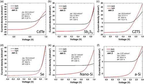
As shown in Figure 1, all these devices present VOC values higher than 700 mV and FF values between 50 and 60%. The series and shunt resistances, RS and RSH, estimated from dark and light measurements are shown in Table I (along with the saturation current density J0 and diode ideality factor n). At first, it is interesting to note that the purchased a-Si minimodule presents the highest RSH value (3 MΩ cm2), together with a high RS value (252 Ω cm2). This device has been specifically designed for indoor applications, but a high RS value appears a priori surprising, even if it could be simply the result of the electrical interconnection. The other devices present lower RSH values, from 21.4 kΩ cm2 for the nano-Si, up to 1 MΩ cm2 for the Se. Another interesting parameter is the saturation current density, which gives information about the recombination processes and especially about the current leakage of the device. Looking at these values, the lowest J0 is achieved with the a-Si minimodule, followed by the Se device. A more detailed discussion on these parameters will be provided in the next section.
| R S (Ω.cm2) | R SH (Ω.cm2) | J 0 (A/cm2) | N | |
|---|---|---|---|---|
| a-Si (dark) | 252 | 3.07E + 06 | 3.52E-12 | 5.13 |
| a-Si (light) | 197 | n/a | n/a | 14.17 |
| CdTe (dark) | 6.0 | 3.16E + 05 | 5.60E-08 | 2.36 |
| CdTe (light) | 2 to 12 | n/a | n/a | 6.01 |
| CZTS (dark) | 2.50 | 1.34E + 05 | 2.08E-09 | 1.88 |
| CZTS (light) | 0.88 | n/a | n/a | 3.64 |
| nano Si (dark) | 59.0 | 2.14E + 04 | 1.02E-07 | 3.71 |
| nano Si (light) | 5.39 | n/a | n/a | 5.80 |
| Sb 2 S 3 (dark) | 1.30 | 2.32E + 05 | 4.25E-10 | 1.73 |
| Sb 2 S 3 (light) | 0.94 | n/a | n/a | 4.90 |
| Se (dark) | 1.27 | 1.13E + 06 | 2.51E-10 | 1.76 |
| Se (light) | 1.22 | n/a | n/a | 3.73 |
4 Devices under Indoor Illumination Conditions
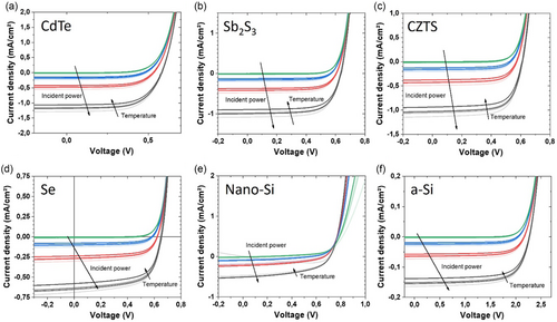
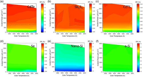
Figure 2 shows the J–V characteristics obtained under indoor illumination conditions, corresponding to the 20 different temperature and intensity spectra, with clear trends for all the investigated devices. As expected, all of them show a drastic decrease in the JSC compared to AM1.5G. At the highest incident powers (around 3 mW cm−2), the devices with higher JSC at AM1.5G still perform better, but with a clear reduction, as all of them generate currents around 0.9–1.2 mA cm−2. The current is even further decreased with the color temperature of the light. At lower incident powers, the situation seems drastically different. To better visualize the other optoelectronic properties of the devices under indoor illumination conditions, figures S2–S7 show the mapping plots of the optoelectronic parameters for the CdTe, Sb2S3, CZTS, Se, nano-Si, and a-Si solar cells, as a function of the incident power and color temperature. This representation allows to identify easily any strong dependance either on incident power or on color temperature. In the case of CdTe, VOC and FF remain high until 500 µW cm−2, with the overall efficiencies remaining quite high until 500 µW cm−2. Color temperature plays a secondary role, with cooler spectra (lower temperature) favoring slightly better JSC and efficiency. For CZTS, the behavior is quite similar to CdTe, the device maintaining relatively good VOC, FF, and efficiencies values until 500 µW cm−2, with almost no dependency on color temperature. For Sb2S3, the behavior is quite similar, with the main difference being FF, remaining high until values lower than 500 µW cm−2, leading to very high efficiencies until ~ 250 µW cm−2. A small dependency on source temperature can be observed for warmer temperatures. For the Se, the behavior is closer to Sb2S3, but with very high VOC, FF, and efficiencies values, until incident power of ~ 250 µW cm−2, and without dependance on source color temperature. For the nano-Si, good VOC values are obtained until 750 µW cm−2, but FF and efficiencies decrease below 2 mW cm−2, with a small dependance on temperature, with warmer spectra (higher temperature) favoring slightly better JSC and efficiency. a-Si has a behavior similar to Se, with high values of VOC and FF remaining at almost any illumination conditions and very low dependency on color temperature.
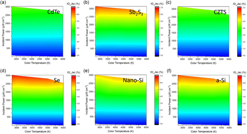
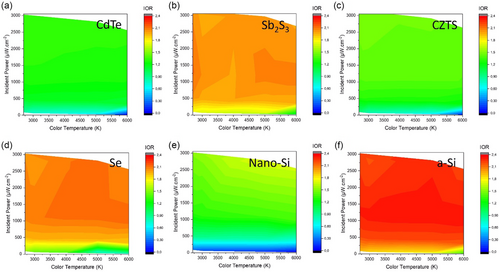
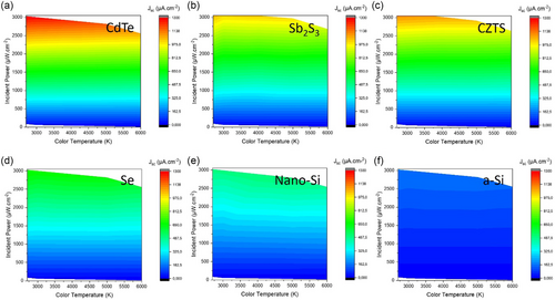
To better compare the optoelectronics parameters between the different technologies, Figures 3–4 present the indoor to output ratios relative to VOC, JSC, FF, and efficiency, while Figures 4–5 show the absolute values measured in indoor conditions. As previously mentioned, the JSC is higher for CdTe, Sb2S3, and CZTS, for relatively high incident powers, but drops drastically below 2 mW cm−2, as shown in Figure 6. In contrast, the low current achieved for the a-Si is maintained at any illumination conditions. Se and nano-Si have higher currents than a-Si, although they show a small reduction under lower illumination powers. In contrast when looking at the IOR JSC ratio (in %), in Figure 3, the best relative retention of JSC is observed for the Se and a-Si devices, retaining 6.8% and 6.5%, respectively, of their JSC under AM1.5G. Other devices perform less favorably, with values of 6% (Sb2S3), 5.5% (nano Si), 4.7% (CZTS) and 4% (CdTe). These results corroborate the relevant role of both shunt resistance (that ought to be > 1 MΩ/cm2) and saturation current density (that ought to be lower than 10−10 A/cm2) to improve the device performance at very low illumination conditions.
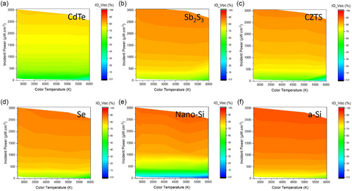
Regarding the VOC, most of the devices retain a high percentage of their VOC under indoor illumination, but the highest absolute values are achieved with a-Si, nano-Si, and Se devices, as shown in Figure 7. CdTe and CZTS show the highest relative voltage losses at indoor illumination. Looking at the indoor to outdoor VOC ratio (in %), the a-Si device shows the best performance, maintaining 60–90% of its VOC across all conditions, indicating excellent voltage stability even under low-light scenarios. The other devices also perform well, with retention ranges of 25–80% for CdTe, 55–86% for Sb2S3, 17–85% for CZTS, 47–87% for Se, and 3–88% for nano-Si (3% at the lowest illumination for 6000 K).
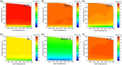
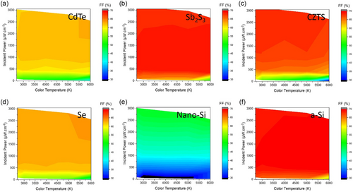
Interestingly, the FF is often higher under indoor illumination than under AM1.5G conditions for most devices, except for the nano-Si device, which shows a slight reduction. The absolute values are shown in figure S9, and the highest values are achieved with a-Si and Sb2S3. Looking at the IORs for the FF, in Figure 8, the values range between 80–120% for CdTe, 56–117% for Sb2S3, 47–113% for CZTS, 75–106% for Se, 63–93% for nano-Si, and 94–117% for a-Si. This suggests that, apart from nano-Si, the other devices exhibit better carrier collection efficiency or reduced resistive losses at indoor illumination.

When comparing the efficiencies achieved in indoor conditions, shown in Figure 9, the absolute values are higher for CdTe, Sb2S3, and CZTS which show efficiencies > 15%, significantly higher than the values achieved for a-Si devices. It is important to remark that these results are higher than SoA a-Si from indoor PV industry (typically with efficiencies below 10%) [23, 24–25] and higher than best-performing lead-free perovskite cells (about 13%) [26-28]. Considering that this is achieved with devices that are still not optimized for indoor illumination conditions, it corroborates the potential of these technologies for achieving high device efficiencies indoors. On the other hand, improving the devices performance under lower illumination conditions is strongly related to the need to improve both shunt resistance and saturation current densities. Se solar cells, even with relatively lower efficiencies, show higher device resilience to changes in the illumination power and color temperature, which is in line with the better RSH and Jo values (relatively close to those from SoA optimized a-Si), as discussed in the next section. In this case, and even if device efficiencies are similar to those achieved within a-Si, the devices show a higher JSC overcoming one of the main current limitations of a-Si technology. On the other hand, the lowest efficiencies achieved within nano-Si devices are strongly related to the very low RSH and high Jo values, which ought to be significantly improved. Even so, it is interesting to remark the high VOC values achieved within these devices, in spite of their very low RSH value, which could be even improved by increasing the absorber bandgap by incorporation of C in the nano-Si layer, as discussed earlier.
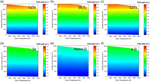
Finally, another aspect to evaluate the different investigated technologies is the power generation density (PGD), which basically refers to the capability offered by PV harvesters to either power directly an IoT device or support a rechargeable battery or supercapacitor. The absolute PGD values obtained for the different devices are shown in Figure 10, clearly highlighting the potential of CdTe, Sb2S3, and CZTS, particularly under indoor conditions higher than 1 mW cm−2. These results demonstrate the potential of the proposed technologies to convert indoor light efficiently into electrical energy achieving high power outputs. To further elucidate this point, Figure 11, 12 compares the PGD values of different devices with the power consumption density (PCD) of IoT devices or rechargeable batteries.
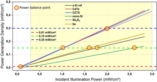
In this figure different power demands are represented (specifically 0.01, 0.15, and 0.3 mW/cm2) together with the PGD values of the different technologies, revealing the minimum light intensities needed for each device to function. For the lower power demand (0.01mW to operate), the PGD exceeds the PCD across the entire indoor light intensity range. This indicates that all the PV devices can effectively power this system even under very low illumination conditions, with sufficient energy to meet the device's operational needs and potentially store excess energy. IoT devices with higher power demands, such as Device 2 (0.15mW) and Device 3 (0.30mW), require more intense illumination to reach the power balance point where PGD equals or surpasses PCD. For the middle power demand, this threshold is approximately 1mW cm−2 for CdTe, CZTS, and Sb2S3 and 1.6 mW cm−2 for Se, 1.7 mW cm−2 for a-Si, and more than 2.5 mW cm−2 for nano-Si. This indicates that CdTe, CZTS, and Sb2S3 are able to deliver the right required power outputs at lower lighting than the other technologies. Similarly for the highest power demand (0.30 mW/cm2), these chalcogenide technologies can still operate indoor. Se devices perform slightly better than SoA a-Si (mainly thanks to the higher generated current), while nano-Si devices can still operate for powering the lower power demand devices (Device 1, 0.01 mW) at the higher indoor power intensities. In this case, optimization of the device architecture is still required to improve both RSH and J0.
4.1 R SH, RS, and J0 for Indoor
The indoor performance of the investigated devices reveals clear correlations with the resistances RSH and Rs reported in Table I. Devices with higher RSH values, such as the a-Si minimodule (3 MΩ cm2) and Se device (1 MΩ cm2), demonstrate superior resilience under low-light conditions. High RSH minimizes leakage currents, which is particularly beneficial under reduced illumination where recombination losses can significantly affect performance. It is also noteworthy that these two devices exhibit the lowest J0 values.
Conversely, the RS values also play a critical role. A high RS, as observed in the a-Si device under dark conditions (252 Ω cm2), may initially seem detrimental due to increased series resistance losses. This high RS could also result from the electrical interconnection and associated resistive losses. However, under indoor illumination, this characteristic may reduce the carrier collection rate, thereby maintaining stable VOC and FF values. This is corroborated by the a-Si device remarkable IOR of FF and efficiency, suggesting reduced resistive losses under these conditions. This clearly indicates that RS has a reduced impact on performance for indoor applications.
Devices such as Sb2S3 and CZTS, which also exhibit relatively high RSH values, display similar resilience in maintaining high efficiency and FF under indoor illumination, underscoring the critical role of shunt resistance in minimizing current leakage. In contrast, CdTe, which has even a better RSH than Sb2S3 and CZTS, experiences more pronounced drops in performance, particularly in JSC and efficiency at low incident powers. This appears to be related to J0, as CdTe exhibits one of the highest values (and also probably to the bandgap values of the materials, being respectively of 1.4 and 1.5 eV, not optimized for indoor). This indicates that all Rs, RSH and J0 must be optimized for indoor applications. Interestingly, the interplay between these parameters becomes apparent when examining the nano-Si device: while it exhibits a notable decrease in FF and efficiency below 2 mW cm−2 which is supposed to be mainly due to low RSH, the device also exhibits a high RS and relatively high J0.
4.2 Challenges and Perspectives
As we have seen, shunt resistance plays a pivotal role in the overall performance of PV devices under low-light conditions. High RSH values are desirable as they minimize leakage currents and improve the open-circuit voltage and FF. However, several factors can lead to lower RSH values, adversely affecting device performance. Among them, the presence of defects or imperfections in the device structure, including material defects in the different layers, manufacturing defects like cracks or scratches, voids or weak adhesion between layers, including contamination from particle or chemical residues and interfacial defects, can lower the RSH. More specifically to thin layers, one of the primary causes of reduced RSH is the presence of pinholes in the absorber layer or in the selective contact layers of the device. Pinholes create unintended electrical pathways that allow current to bypass the photoactive regions, resulting in increased leakage currents and reduced device efficiency. These defects can arise from nonuniform deposition processes or material imperfections during fabrication, creating weak spots or areas with reduced insulation (also affecting J0). Additionally, material incompatibility between the absorber and the selective contact layers can form localized regions with poor electrical characteristics, effectively creating shunts. Variability in the thickness, roughness, and uniformity of these layers can exacerbate this issue, particularly in thin-film technologies, and especially when high-temperature processes are involved in the fabrication process, which can easily induce mechanical stresses and delamination. Regarding this point, it is interesting to note that Sb2S3, nano-Si, and Se involve low temperatures processing, which could be favorable to improve RSH. However, further studies would be needed to understand the origin of shunt for each technology, as different reasons could be involved. In that regard, an interesting aspect to consider would be analyzing the variation of the RSH under light illumination to better understand the origin of shunt [28].
Optimizing the bandgaps to a range of 1.7–1.9 eV is crucial for all the considered technologies, as this is currently not the case for CdTe and CZTS. Modeling of an ideal p–n junction in the radiative limit has been performed varying the bandgap and source temperature of the light [29] and preliminary results show that materials with Eg within the range 1.7–1.9 eV are optimal for performance and less sensitive to color temperature under indoor conditions (more results will be published in another study providing specific guidelines for indoor PV). This explains why CdTe and kesterite present a small dependency with color temperature that could be reduced with an optimized bandgap together with a higher performance.
Another important aspect to consider relates to the selective contact layers. In the above considered devices, only CZTS employs CdS as the electron-selective contact. This layer has a relatively narrow bandgap and can lead to significant parasitic absorption of photons, not contributing to the generated photocurrent, especially under low incident power. More generally, selective contacts designed for outdoor PV devices (and lower absorber bandgaps) may not efficiently capture the lower-energy photons prevalent indoors, resulting in suboptimal charge extraction and increased recombination losses. All the other devices employ electron-selective contacts that should avoid parasitic absorption.
All the considered thin-film technologies in this work have high potential for indoor use with proper optimization. This will require employing selective contact materials with wider bandgaps and lower parasitic absorption that can enhance light utilization. Moreover, advanced deposition techniques (such as atomic layer deposition or chemical vapor deposition) minimizing the formation of defects (and ensuring high uniformity) could help reducing pinholes formation and improving the RSH. The use of adequate passivation layers could also be a way of further improving the RSH and overall indoor performance. Understanding and mitigating the origins of low RSH and adapting selective layers to the different technologies will ensure improved performance, stability, and overall performance indoors.
While traditionally considered a limiting factor for outdoor applications, high Rs values can be less critical indoors, opening the door to using devices with higher RS without significantly compromising performance, but offering high resilience in a wide range of low-light conditions. This flexibility is especially relevant for monolithic integration, where high electrical conductivity of electrodes and contacts is not anymore a requisite as for outdoor. As many of the indoor devices are expected to substitute small batteries (most of them with voltages around 1.2–4.2 volts), interconnection in series of several individual cells becomes a requisite. This configuration plays in favor of the thin-film technologies considered, which could accommodate higher RS values while still achieving the required voltage output, thus broadening the scope of materials and designs suitable for indoor energy harvesting.
5 Conclusion
This work reports the comparative analysis of the optoelectronic behavior of several inorganic thin-film PV device technologies (CdTe, kesterite, Sb2S3, nano-Si, and elemental Se) that appear as potential interesting candidates for indoor applications, due to their suitable bandgap energies and very high robustness and stability, using a consistent characterization methodology that encompasses the needs of indoor PV (with variations in light intensity, i.e., irradiance and color temperature), including a benchmark with commercial SoA a-Si devices. The results show that these devices perform surprisingly well indoors, with device efficiencies higher than 15% for CdTe, Sb2S3, and CZTS. It is important to remark that these results are achieved within devices that are still not optimized for indoor illumination conditions, and this explains the deterioration of the device performance observed at lower illumination power. Improving the performance of the devices under lower illumination conditions is strongly related to the need to improve both shunt resistance and saturation current density. Se solar cells, even with relatively lower efficiencies, show higher device resilience to changes in the illumination power and color temperature, which is in line with the better RSH and J0 values (relatively close to those from SoA optimized a-Si). In this case, the devices show a higher short-circuit current density than a-Si, overcoming one of the main current limitations of a-Si technology. On the other hand, the lowest efficiencies achieved within nano-Si devices are strongly related to the very low RSH and high J0 values, which ought to be significantly improved. Even so, it is interesting to remark the high VOC values achieved within these devices, in spite of their very low RSH value, which could be even improved by increasing the absorber bandgap by incorporation of C in the nano-Si layer, as discussed above. This study confirms that RSH, RS, and J0 emerge as critical parameters influencing the resilience under indoor lighting conditions. High RSH values, as observed in a-Si and Se devices, are essential for minimizing current leakage losses, while proper control of RS and J0 helps maintain high VOC and FF values in indoor conditions. The study emphasizes the need to optimize these parameters to maximize the performance of the investigated technologies for indoor applications. Moreover, low-temperature processing is identified as a key advantage in avoiding defects such as pinholes that degrade RSH. This highlights the importance of adapting and optimizing the technologies to the specific indoor conditions use.
Acknowledgments
The authors from UPC and IREC belong to the Micro and Nano-Technologies for Solar Energy Group (MNT-Solar) Consolidated Research Group of the “Generalitat de Catalunya” (2021 SGR 01286) and are grateful to European Regional Development Funds (ERDF, FEDER programa Competitivitat de Catalunya 2007–2013). M.P. and A. T. acknowledge the project SELECTRON (CNS2023−14817), funded by MCIN/AEI/10.13039/501100011033/ NextGenerationEU/PRTR. Z. J. thanks financial support from Spanish Ministry of Science, Innovation, through the Ramon y Cajal fellowship (RYC2021-033239-I). M.P. and Y.S. acknowledge the project ENPOWER (PCI2024-155100−2 and PCI2024-155054−2) from the CETP-Partnership Program 2023 funded by MCIN/AEI/10.13039/501100011033/ FEDER, UE. Y.G. thanks the European Union's 616 Horizon 2020 research and innovation programme under the Marie Skłodowska-Curie grant agreement 618 no 10115148. S.G. thanks the Serra Húnter programme. E.S. is grateful to ICREA Academia program. R.S. thanks FWO for funding through the Fundamental Research PhD Fellowship (1178024N). A.P.R., M.P., and I.C. thank InnoPV (PID2022-140226OB-C31 and PID2022-140226OB-C32), funded by MCIN/AEI/10.13039/501100011033/ FEDER, UE. A.J.A, A.P.R, N.S, I.O.A acknowledge the project ACT-FAST (PCI2023-145971−2, VHE24004) funded by CET Partnership, the Clean Energy Transition Partnership under the 2022 CET Partnership joint call for research proposals, cofunded by the European Commission (GA N°101069750) and funded by Spanish MCIN/AEI/10.13039/501100011033/ FEDER and by Estonian Research Council, agreement no. MOB3PRT2. N.S, I.O.A acknowledge the projects TK210/TK210U8 “Center of Excellence in Sustainable Green Hydrogen and Energy Technologies” funded by the Estonian Ministry of Education and Research and EU Horizon 2020 project 952509-5GSOLAR.The article is based upon work from COST Action Research and International Networking on Emerging Inorganic Chalcogenides for Photovoltaics (RENEW-PV), CA21148, supported by COST (European Cooperation in Science and Technology).
Conflicts of Interest
There are no conflicts to declare.
Open Research
Data Availability Statement
The data that support the findings of this study are available from the corresponding author upon reasonable request.


