Solid-State Nanopore Array: Manufacturing and Applications
Abstract
Nanopore brings extraordinary properties for a variety of potential applications in various industrial sectors. Since manufacturing of solid-state nanopore is first reported in 2001, solid-state nanopore has become a hot topic in the recent years. An increasing number of manufacturing methods have been reported, with continuously decreased sizes from hundreds of nanometers at the beginning to ≈1 nm until recently. To enable more robust, sensitive, and reliable devices required by the industry, researchers have started to explore the possible methods to manufacture nanopore array which presents unprecedented challenges on the fabrication efficiency, accuracy and repeatability, applicable materials, and cost. As a result, the exploration of fabrication of nanopore array is still in the fledging period with various bottlenecks. In this article, a wide range of methods of manufacturing nanopores are summarized along with their achievable morphologies, sizes, inner structures for characterizing the main features, based on which the manufacturing of nanopore array is further addressed. To give a more specific idea on the potential applications of nanopore array, some representative practices are introduced such as DNA/RNA sequencing, energy conversion and storage, water desalination, nanosensors, nanoreactors, and dialysis.
1 Introduction
Nanopore is a nanoscale hole or channel with a diameter/width between 1 and 100 nanometers, usually in a free-standing membrane.[1-3] DNA/RNA (deoxyribonucleic acid/ribonucleic acid) sequencing based on nanopore could be tracked since decades ago. Kasianowicz et al. demonstrated that DNA and RNA molecules could go through a nanoscale pore and the electrical signal exhibited the diversity, therefore, this phenomenon underpins the approach for DNA/RNA sequencing.[4] By continuous effort devoted worldwide since then, nanopores for detection of molecules especially for DNA and RNA sequencing has achieved significant progress meanwhile addressing the other potential applications such as molecule filtration, toxicity test, supercapacitor, nanoparticle separation, water purification, and energy conversion.[5-7] Thus, diversified techniques have been developed for manufacturing single nanopore although it is still challenging for industrial practices nowadays due to the unsatisfactory scalability and efficiency of the processes. Furthermore, the performance of the nanopores is still needed to be further improved, such as the compatibility and physicochemical properties for the detection of biological molecules.[8]
Nanopores are not only an artificial product, but also widely exist in cells reported by Kiesinger et al. that might predate an evolution of lifestyle.[9] Currently, the only commercial nanopore sensor is provided by the Oxford Nanopore Technologies which uses a large molecule with a hole inside. Compared with such a biological solution, the solid state nanopore is more robust and durable, presenting lower requirements on the preserve and application environment, and more compatible with scalable engineering manufacturing technologies. However, there are few commercial products available due to the lack of efficient and cost-effective manufacturing process chain for solid state nanopores.[2, 3, 10] For single nanopore, some major limitations exist for practical applications due to the fact that only one small hole can act each time which also significantly restricts the productivity. Thus, researchers are exploring ways in manufacturing of nanopore array in the recent years, and the exceptional performance of nanopore array has been gradually verified. For example, it is reported that the nanopore array has better performance in DNA/RNA sequencing due to the improved electron resolution when DNA/RNA fragments translocate through the nanoholes.[11] However, insufficient attention has been given to the nanopore array.
There are some review papers that have summarized the research progress on manufacturing of solid-state nanopore. For example, Yuan et al. summarized the solid-state nanopore manufacturing technologies during recent decades, and it was proposed that nanopore could not be massively produced at low cost and high efficiency so far.[12] Xue et al. reported the recent progress in Nature Reviews Materials around the nanopore sensors and specifically introduced the applications of nanopore sensors.[13] He et al. reviewed a variety of nanopore-based materials and their applications.[14] Although the previous reviews did make a good summary on the manufacturing or application of solid state nanopore, few papers are found to focus on the fabrication and application of nanopore array, let alone the large area nanopore array. Moreover, it was rarely discussed in these reviews that if the manufacturing technologies for single nanopore could be applied to nanopore array with sufficient efficiency and where the major challenges lie. Therefore, in this review, the authors summarize and emphasize the recent development of nanopore array fabrication where some unconventional methods and emerging methods that were usually omitted in previous reviews, such as nanobubble based electrodeposition and machining learning assisted chemical etching, have also been included to indicate new possibilities. Simultaneously, discussions are organized on the suitability of some conventional nanopore manufacturing technologies for scaling up to nanopore array fabrication, and some key barriers are identified.
This review generally focuses on the nanopore array including manufacturing technologies, materials, mechanisms, the challenges, and opportunities for future development, to make a different perspective. To further demonstrate the value of nanopore array and the stringent manufacturing requirements raised by practice, some typical applications are listed including DNA/RNA sequencing, energy conversion and storage, water desalination, nanosensors, nanoreactors, and dialysis. At last, some latest advancements on large area nanopore array fabrication are briefly introduced addressing the challenges in this field.
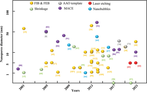
Figure 1 charted some representative achievements in nanopore manufacturing clued with diameter/width of the nanopores in the last 20 years. Focused ion beam (FIB) and focused electron beam (FEB) were first applied to the nanopores fabrication in 2001, it can be seen that numerous nanopores fabrication approaches developed are related to FIB and FEB from the year of 2005–2015 whose nanopore sizes were below 15 nm, and a large number of articles on nanopores were published since then. At the same year, the nanopore shrinkage phenomenon was found which offered the possibility to decrease the size down to ≈1 nm. In 2017, nanopores were successfully achieved to the size below 1 nm. As shown in the image, a wide range of efforts have also been made from the other pathways, which emerged new technologies and outputs continuously. One of the main reasons is that current manufacturing technologies are still far away from supporting commercialization due to the low efficiency and high cost, which forms a key driver to the research advancement. The second enabler is the requirements from industry on more robust and intelligent nanopore sensors, especially in the form of large area nanopore array. The third reason attributes to the appearance of new technologies, such as the machine learning (ML) and laser techniques, which provide new possibilities for producing the nanopore sensors.
2 Manufacturing of Nanopore Array
Substrates made of different materials have been used to fabricate the single nanopore or nanopore array structure, such as silicon-based substrates (Si; SiO2; SiN), glass substrates, alumina membranes, graphene membranes, metal oxide (HfO2; Al2O3; TiO2) membranes, polymers (ployimide; polycarbonate; polyethylene terephthalate (PET)), and composite membranes (MoS2/SiNx; Si3N4/SiO2; Graphene/Al2O3), producing various physicochemical properties to support different applications.[9, 15-37]
The fabrication and synthesis of nanopore array are more complex and trickier compared to the fabrication of single nanopore. In this section, several pathways are introduced including ion and electron beam lithography, laser etching, plasma-based thin film deposition, electrodeposition, electrochemical anodization, and chemical etching.[5, 7, 38-44] The systematic briefing of typical manufacturing technologies are concluded in Table 1. To be specific, the high energy beam lithography is a straightforward approach to create the desired dimension of nanopores on diversified materials. This approach can be applied on both single solid state nanopore and nanopore array. Laser assisted nanopore drilling was invented recently but the whole crafts in nanopore fabrication is relatively complex. Both methods can achieve the uniform nanopore distribution with good controllability, but nanopore size can only reach 8 nm at minimum. Another major obstacle is that the efficiency is too low to fabricate nanopore array. Some other technologies reviewed below, like electrochemical deposition, anodization, and wet (chemical) etching, even combination with ML, are promising to achieve large area nanopore array fabrication but still exhibiting limited qualification on nanopore shape, dimension, and distribution. The hybrid fabrication uses multiple steps, combining the advantages of various means and providing new possibilities.
| Method | Branches of method | Advantages | Disadvantages | Distribution of pore size | Refs. |
|---|---|---|---|---|---|
| Ion and electron beam lithography | The pore size and shape at local spot can be controlled precisely. Real-time monitoring of pore size during manufacturing. The nanopore array distribution is uniform. | Time-consuming for nanopore array. Costly high-energy beam device is needed, which could destroy the nanopore substrate potentially. | 3 [Å] −280 [nm] | [15, 17, 38-40, 45-48] | |
| Laser etching | Quick fabrication. Automated without user intervention by a nanopore laser drilling algorithm (NLDA). In alkaline conditions, the fabrication rate will be increased even at lower laser radiation intensity. | Need to be running under the optical set-up in alkaline conditions, which produces laser and at the same time supervise nanopore formation, so the entire device is complex. | 2.5–5 [nm] | [41, 42] | |
| Nanopore shrinkage | High-energy beam | In-suit nanopore shrinkage. Real-time monitoring on pore size and shape. | Single nanopore shrinkage under high energy beam so the efficiency is relatively low for nanopore array. High-energy beam may damage the substrate or structure. | 0–5.3 [nm] | [15, 57, 58] |
| Direct thermal heating | Multiple nanopores shrink at the same time, so realizing high efficiency potentially. | The diameter of the nanopore must be smaller than the thickness of the membrane, otherwise, the nanopore would expand. | 3–20 [nm] | [59] | |
| Deposition (chemical vapor deposition (CVD)/physical vapor deposition (PVD)/atomic layer deposition (ALD)/Electron deposition) | Applied in a wide range of applications with multiple choices of devices. | Increasing thickness of substrate. Destroy the geometry of nanopores. | 2–22 [nm] | [60-63] | |
| Electrodeposition based on nanobubbles | Generation of a large area of nanopores by fast fabrication. | Nonuniform nanopore geometry, size, and distribution, difficult to control. | 1–165 [nm] | [64-67] | |
| Electrochemical anodization | Applicable to nanopores with larger thickness from nanometer scale to micrometer scale. High nanopore density, shape and size are relatively uniform. | Need mask. Only applicable to some limited materials. The membrane is thick. | 21–113 [nm] | [16, 28, 69, 73] | |
| Wet etching | Chemical etching | High efficiency in fabrication of nanopore with thick membrane. | The pre-etched pattern is required. Long etching time. | 13.2–38 [nm] in average | [75, 76, 78] |
| Metal assisted chemical etching (MACE) | Low-cost for fabrication of nanopore array. Appliable to microscale thickness to nanoscale membrane. | The shape and size affect the pore geometry. | 10–300 [nm] | [44, 82, 84, 85, 92, 93] | |
| Hybrid fabrication | The nanopore size can be customized in a wide range. Flexible to combine different techniques for forming a suitable process chain. Each step can be efficiently designed and controlled. High quality nanopore array structure. | Cumbersome consideration and design of process chain. Complex control of manufacturing process. More potential risks are introduced. | 80–150 [nm] | [97] |
2.1 Ion and Electron Beam Lithography
From the last two decades, researchers begun to learn from nature and the first solid state nanopore was fabricated by Li et al., who fabricated a single nanopore with 1.8 nm in dimension on the Si3N4 membrane by low energy Ar+ ion beams.[15] Similarly, the nanopores could be drilled by electron beam as well. Wu et al. reported the drilled nanopore by FEB in a SiN/SiO2 wafer.[40] The nanopore was nearly 5 nm in size completed in 6 min. Lo et al. also reported that by FIB multiple nanopores were fabricated simultaneously on SiN with asymmetrical shapes and the minimum size reached nearly 5 nm.[17] There are other symmetric nanopores with various shapes like circular or rectangular produced by FIB on different membranes. Biance et al. reported holes below 15 nm on SiC membrane with thickness between 10 and 100 nm.[45] Morri et al. fabricated irregular nanopores about 10 nm in suspended graphene films.[46] Russo and Golovchenko have reported a pore formation by ion and electron irradiation directly into the surface of graphene. They explained the formation of nanopores of graphene attributed to the disruption by electron beam and nucleation atomically.[47]
Although ion beam lithography has been applied in the fabrication of single nanopore extensively, single beam source would largely limit the efficiency for manufacturing nanopore array. Kim et al. took the measure of a dual source FIB instrument (Helios Nanolab 600, FEI corporation) to drill an array of nanopore structure.[39] The entire membrane consisted of 3721 truncated cone nanopores in an area 30 × 30 µm2, displaying the top and bottom diameters nearly 280 and 173 nm, respectively. A large quantity of nanopores fabricated were successfully arranged uniformly (Figure 2A).[39] However, in this article, the authors did not clarify the duration spent on manufacturing such a big number of nanopores.
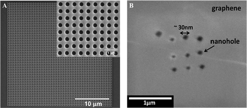
Besides, gallium (Ga) ions milling was first applied to fabricate single nanopore by controlling different drilling currents to obtain various sizes of pore structures.[49] Fürjes further used this technique to fabricate the nanopore array with diameters 30–80 nm on modified Au/SiNx/Au film.[38] This computer-controlled FIB system provided a high efficiency for fabrication of nanopore array. It was reported that the quickest fabrication was achieved in about 3 s and a nearly 20 nm nanopore was formed. This study proved the conformity of the pore geometry and promoted the reliability of fabrication because of an additional front size metallization and the electrical grounding of the metallized surface that benefits releasing charging effects.[38] More importantly, the conformity of the nanopores would largely increase the sensitivity of molecule detection. Md Ibrahim and Hashim also used the similar FIB method to fabricate a 3 × 3 nanopore array with a diameter about 30 nm on graphene/Si3N4 bilayer, the SEM image was shown as Figure 2B.[48] In fact, the nanopore array fabricated by FIB milling would form relatively large size. On the contrary, to fabricate the nanopore array with smaller size, the shapes would become irregular and errors that might be much larger than 10 nm. Even though the attached conductive layer like Au or graphene helped mitigate this issue, the thickness of the thin film would be invisibly increased.
Apart from Ga ions milling technique, there is also neon assisted technology called neon beam lithography (NBL), developed for nanoscale device fabrication. Winston et. al reported the gas field ionization source (GFIS) assisted by Ne ions, instead of Ga or He ions, as Ne ions are higher than He and Ga ions in mass weight thus lead to smaller resist interaction volume for lithography.[50, 51] The NBL is more suitable for semiconductor circuit editing than helium beam lithography (HBL) because of its higher sputtering rate and higher resolution.[52, 53] Besides, the HBL is prone to destroy the substrate.[53, 54]
2.2 Laser Etching
Gilboa et al. designed a laser etching assisted machine for nanopore fabrication which provided a fast way to drill nanopores and evidenced an ≈5 nm pore after 15 s laser exposure.[41] Besides, it was also discussed the effects of pH values and clarified that higher pH values would increase the speed of etching compared to that pH < 7. The results of this study open a horizon for drilling nanopores by photoactivation-assisted etching at specific location. More recently, Zvuloni et al. from the same group has fabricated ≈5 nm nanopores by laser processing based on further advancing Gilboa's work.[41, 42] They developed a multistep control algorithm-nanopore laser drilling algorithm (NLDA) which constitutes three constant processes: thinning, drilling, and polishing. The new fabrication algorithm can fabricate both smaller and larger nanopores by adjusting NLDA. More importantly, such a technique could fast work without user intervention and easily form nanopore array at specific position, which is important for the potential application of nucleic acid and protein sensor.
Laser assisted processing of nanopores emerged in the recent three years. Although the works mentioned above have achieved a precise fabrication of nanopores, the cost is still high and experimental facilities are complex, which implies rigorous working condition and complicated process control consisting of various variables. Laser assisted processing is still a young fabrication method but provides a promising solution for fast fabrication of nanopore array.
2.3 Nanopore Shrinkage
Shrinkage is an effective way to further reduce the size of nanopores, especially considering that most existing techniques are still facing rigorous challenges on directly achieving the nanopore size approaching 1 nm. Especially for forming nanopore array, shrinkage potentially provides a possible way to treat multiple nanopores simultaneously, thus might be able to support a scalable industrial practice. There are generally several methods leading to the nanopore shrinkage which could be classified into two categories. One category can produce the alterations of crystal lattice caused by exposed to electron or ion beam irradiation or thermal heating. The other utilizes material addition like atomic layer deposition (ALD) deposition which achieves atomical-layer deposition, as well as physical vapor deposition (PVD)/chemical vapor deposition (CVD) that employs at the nanometric scale to physically reduce the pore size.[55, 56]
Electron or ion beam can be used to drive nanopores shrinkage.[15, 57, 58] If the nanopore is exposed to the ion-beam or electron beam continuously, the pore size would be decreased constantly until it vanishes. So far, there are two different views that explain this hole closing phenomenon. One attributes to a stressed viscous surface layer during the ion beam irradiation that enhances layer to relax. Another explains incident beam can both create and annihilate excess, independent, and mobile surface “adatoms.” The active adatom diffusion by high temperature can also be accounted in this category.[15] For example, in Figure 3A, the Si3N4 nanopore dimension was declined from 60 to 1.8 nm under the constant Ar+ beam. In Figure 3B, the SiN/SiO2 nanopore size decreased under the FEB exposure until its closure eventually.[55]
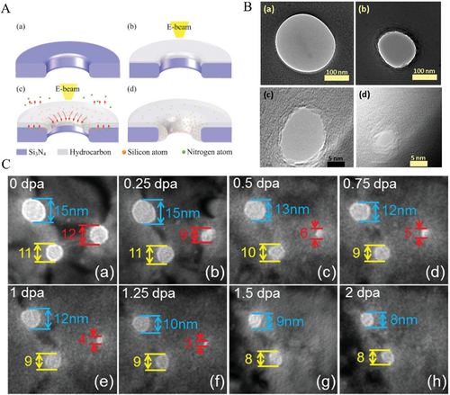
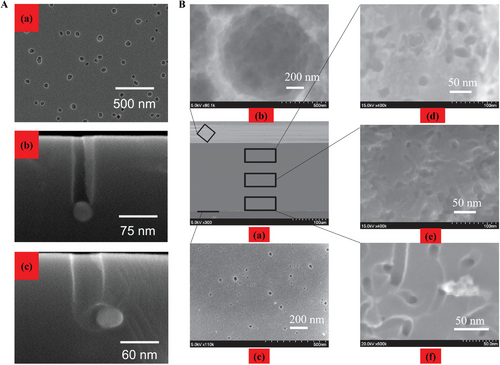
Yuan et al. reported a mechanism of nanopore shrinkage on Si3N4 membrane shown in Figure 3A. Hydrocarbon deposition was produced when there was electron beam irradiation scanned on the surface. The atoms of Si and N diffused into the hydrocarbon layer and simultaneously nitrogen species were pumped away from the system.[57] Li et al. studied Au nanopores under heavy ion beam irradiation but gave an explanation by defect adsorption which led to atomic diffusion. They snapshotted three spots of Au nanopores with diameter of 15 nm (blue mark), 12 nm (red mark), 11 nm (yellow mark) nm, respectively in Figure 3C(a). When the irradiation was exposed as in Figure 3C(b)–(h), the diameters of nanopores decreased continuously until the nanopore disappeared by 1.5 dpa which was marked by red arrows. The other two pores decreased from 15 to 8 nm and from 11 to 8 nm, respectively, due to the effect that atoms of defects diffused into the pores.[58] Asghar et al. reported a shrinking method by direct thermal heating. Figure 3B(a) was the fabricated nanopore with nearly 250 nm in dimension. After thermal processing under 1150 °C, the diameter decreased to about 150 nm after 5 min, and then declined to 20 nm after 10 min, until another 10 min and 40 s, the nanopore diameter was only about 3 nm finally.[59] In the article, the author proposed a model indicates that the membrane of SiO2 would be soften during the high temperature (> 1000 °C), therefore, the free-standing atoms can diffuse to the location with lower free energy.
The other kind of nanopore shrinkage is based on the materials deposition. Such process indicates materials are deposited to the inner surface of nanopores that constantly compress the sizes. There are some useful machines that could achieve the nanopores shrinkage, such as ALD, CVD, and electron deposition. Chen et al. reduced the nanopore size by deposition via ALD.[60] Figure 4A(a) is the TEM image of FIB nanopore and (b) is the image after 500 layers Al2O3 deposition. The size was reduced by nearly ninefold and the shape was maintained as a square as the original. Moreover, Figure 4A(c),(d) showed a nanopore which was about 21.6 nm in diameter by ion beam sculpture and an ≈4.8 nm nanopore after 70 layers Al2O3 ALD deposition. Similarly, Figure 4A(e) was sculpted nanopore which has nearly 7.1 nm in size and (f) was an around 2.0 nm nanopore after 24 deposited layers of Al2O3. Similarly, Spende et al. deposited polycarbonate nanochannels by ALD whose thicknesses varied from 5 to 22 nm.[61] In Figure 4B, from scanning transmission electron microscopy (STEM) images which indicated the nominal thickness of (a) TiO2, (b) SiO2, (c) Al2O3 was 5 nm, the outer diameters were about 18, 31, 42, and 55 nm. It was obviously to see that after mounting (a) TiO2, (b) SiO2, (c) Al2O3 respectively, both STEM and small angle X-ray (SAXS) images confirmed that the diameter of the nanotubes were decreased with a varied degree, compared to the uncoated samples which were illustrated by yellow icons. Wang et al. processed the pore shrinkage by Plasma-enhanced CVD (PECVD), as shown in Figure 4C(a)–(c) which were the SEM images of a single pore, with the initial size 350 nm in (a). After 400s and 600s, respectively, the compressed process was described by the orange dashed lines compared to the white dashed lines, and the shrinkage alterations were shown in Figure 4C(b),(c), respectively.[62] Besides, Ayub et al. obtained the single sub-20 nm nanopores by four-electrode cell equipment (left in Figure 4D). The right part of the SEM images on the right are the initial pore morphology and processed pore by electrodeposition, respectively. The size compressed was around 18 nm.[63]
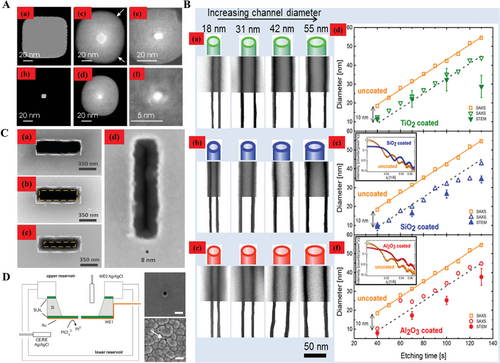
By nanopore shrinkage, the desired sizes could be obtained. However, some problems associated with the approaches mentioned above must be noted here. For the approach by ion or electron beam, the desired nanopore diameter could be precisely regulated by energetic beam. But simultaneously, the fabrication efficiency would be affected by the beam gun which means, by this approach, only a tiny area could be focused on, therefore, not suitable for amending the nanopore array in a larger scale. Ion or electron beam irradiation also result in the condensation of certain elements on the surface, further leading to the physicochemical properties changing. While the thermal heating can solve the problem of shrinking multiple nanopores simultaneously, but a major limitation is that it only works when the diameter of the nanopore is smaller than the thickness of the membrane, otherwise, the nanopore would expand.[3] Although deposition is also possible to tackle multiple nanopores to offer a higher efficiency, the thickness of membrane would inevitably be increased resulting in an increasing length of nanopore channel which might affect the analytic resolution for molecule detection.[3]
2.4 Electrodeposition Based on Nanobubbles
Some innovative views were proposed on fabrication of nanopore or nanopore array based on formation of nanobubbles during the electrodeposition process, although it is basically the inherent phenomenon of the electrodeposition. This provides a promising approach and new possibility for the efficient and cost-effective manufacturing of large area nanopore array.
Hartwig and Klages reported the ordered 2D nanopore array with diameters of nearly 40 nm and center-to-center distance of 120 nm on nickel layer by pulse current electrodeposition. They observed a new self-organization during the electrodeposition and attributed the pore formation mechanism to the hydrogen nanobubble formation and ordering.[64] Hui et al. reported using nanobubbles as a template, electrochemical fabrication of nanopores in polypyrene (PPy) film.[65] The deposition demo plot is shown in Figure 5A(a). The experiment was performed in the predegassed solution of 1 mm pyrrole and 1 mm sulfuric acid, and sulfuric acid diluted solution was working as nanobubble generation electrolyte and sulfuric ions were employed as dopant ions. Their results indicated that at a voltage of −2.0 eV, the lateral width of nanobubbles were 25–115 nm and at a voltage of −1.7 eV, the lateral width of nanobubbles were about 40–165 nm. Besides, the numbers were about 500 and 150 per 25 µm2, respectively.[65] Although nanobubbles are easily formed in large-scale, the size and distribution of nanobubbles are hard to control for uniform formation of nanopore array. Additionally, Elias et al. also reported that hydrogen gas bubbles worked as a template to form zinc oxide (ZnO) porous mesostructures during the electrodeposition, as shown in Figure 5C(a)–(f).[66] The minimum pore dimension was only 1 nm as shown in Figure 5C(e) and maximum pore dimension was 10 nm in Figure 5C(f). Tarabkova and Janda also reported nanopore formation (Figure 5B(a)–(c)) under aqueous phase ascribed to mild and dynamic negative pressure (−10 kPa 5 s−1) that applied to the pre-prepared polystyrene (PS) film. The article showed that the pores formation was related to interaction between the contact angle caused by expansion of nanobubbles and PS interface.[67]
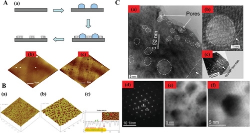
Generally, the methodology of using nanobubbles as a template is believed to be cost-effective in fabricating nanopore array on the film due to its relatively high efficiency. Electrodeposition is a common method for synthesis of new materials that reported by many research papers.[68] However, the nanobubbles formation during electrodeposition has been studied by very limited researchers for manufacturing purpose. Although not much research was found which may imply the difficulties to control the process, Elias et al. has revealed the possibility of producing pores diameter less than 1 nm.[66] In consideration of the promising efficiency and relative low cost of this approach, more efforts are suggested to be devoted along this path especially on the controllable gas release aiming at more uniform nanobubble generation and distribution. Nanobubbles could become a feasible medium to benefit the fabrication of nanopore array.
2.5 Electrochemical Anodization
Anodic aluminum oxide (AAO) is one of the most popular materials employed for the generation of periodic nanostructures.[64] It has been used to synthesize aligned nanopore structures because of its flexibly adjustable morphologies, structural stability at high temperature in organic solvents, uniform pore density and distribution which is usually parallel or perpendicular to the surface with cylindrical shape.[69] Over a decade, AAO nanopore array fabrication has experienced three-step anodization resulting in disordered structures to two-step anodization for self-ordered pore structures, to recent one-step anodic nanopore array of aluminum oxide, that largely reduces the processing time and increases the ordered nanopore domains.[16, 28]
Chen and Zhang reported that AAO nanopore array structure consists of aluminum layer, oxide layer as a barrier layer, and pores layer defined mainly by pore diameter, interpore distance, pore density, and film thickness.[8] They optimized the experimental conditions which was at 40 V (DC) in 0.2 m oxalic acid electrolyte, by two-step anodization lasting for 5 and 15 min, respectively. Then 1D nanopore array was formed that the pore size was 40 nm and pore depth was 500 nm. Ates et al. reported the AAO nanopore array via two-step anodization, obtaining a range of 31–113 nm in size and 3.4–33 µm thick oxide layer.[70] This two-step technology processed samples in two separate electrolytes after the first step anodization at 50 V for 1 h, as schematically shown in Figure 6A.[70] The two electrolytes were defined separately as A and B. As reported,[70] 0.3 m H2C2O4 electrolyte (A electrolyte) and the mixture of water and ethylene glycol electrolyte (V:V = 1:1) blended with A solution (B electrolyte) were adopted. Figure 6B(a)–(f) described the field emission-scanning electron microscopy (FE-SEM) morphologies of nanopore array structures produced by two-step anodization after annealing at 550 °C. (a)–(c) illustrated the FE-SEM images after AAO anodization in A electrolyte for 1, 2, 4 h, respectively. The nanopore diameter increased with anodization time from 1 to 4 h which raised from 41 to 45 nm, and finally reached 97 nm at 4 h. Besides, the thickness of oxide layer also increased from ≈10 µm in 1 h to 17 µm in 2 h, and at last 33 µm in 4 h. Similarly, (d)–(f) illustrated the AAO pore images at different anodization hours in B electrolyte, where the pore sizes determined by FE-SEM morphologies indicated 33, 44, 54 nm for anodization time 2, 4, and 8 h, and the oxide layer thickness was found to be 3.4, 6.5, 22.7 µm, respectively.[70] By comparison, the nanopore array structures made by B electrolyte were denser than that by A electrolyte.

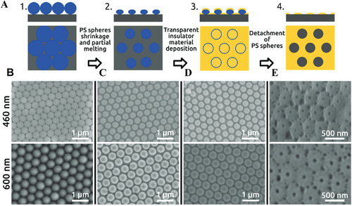
Simultaneously, AAO nanopore array by one-step anodization has been reported. Nanopore array diameter has been affected by many factors: electrolyte type, electrolyte concentration, bath temperature, voltage, current density, and time.[71, 72] Bruera et al. synthesized AAO nanopore array by single-step anodization at near room temperature and explored the relationships between the synthesis condition including electrolyte concentration, temperature, anodization voltage, the current density and the morphologies of AAO films via characterization of pore diameter, interpore distance, pore density, and film thickness.[73] Mínguez-Bacho et al. presented the ordered nanopore array by one-step anodization, via self-assembling of spherical PScolloidal particles and sputter-deposition of SiO2 onto Al substrate, as shown in Figure 7A.[16] The diameters of PS colloidal particles are 460 and 600 nm, respectively, being dispersed on the electropolished alumina substrate. According to Vogel et al., Langmuir–Blodgett method was used, and high-ordered PS particles were formed as a hexagonally close-packed monolayer seen in Figure 7B.[74] After that, the PS particles were shrunk by plasma etching and diameters of both spheres in Figure 7C were decreased. The plasma-etched nanospheres formed nonclosing packed arrangement. Then, the transparent insulator SiO2 was deposited by radio-frequency sputtering technique. Figure 7D describes SEM morphologies after 50 nm thickness SiO2 deposition. Subsequently, PS colloidal particles were detached from the substrate, then left the hexagonal AAO pore structure as seen in Figure 7E. The author proposed in the article that this one-step anodization process had the advantage in reducing fabrication time and increasing the area of ordered nanopore array domains.[16]
2.6 Wet Etching
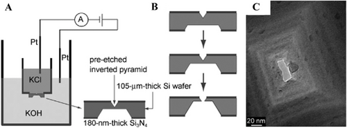
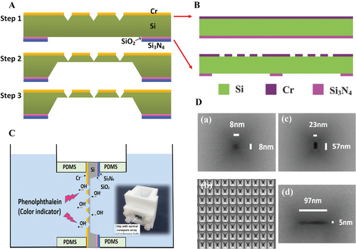
Wet etching, namely chemical etching has been adopted for the formation of nanopores due to the ease of operation and high efficiency. Park et at. reported that a 180 nm thick Si3N4 layer was pre-deposited by plasma-enhanced chemical vapor deposition on the <100> silicon wafer (105 µm) on both sides as an etching layer.[75] Then, they fabricated an inverted pyramid sharp tip on the front side and a truncated pyramid on the back side by Si anisotropic etching in the alkaline solvent consisting of potassium hydroxide (KOH) and tetramethylammonium hydroxide ((CH3)4NOH), as shown in Figure 8A,B. The rectangular nanopore (15 × 38 nm2) after etching can be clearly seen in the Figure 8C.
Moreover, Chen et al. achieved the fabrication of nanopore array with size down to 5 nm by chemical etching via a proposed improved three-step wet etching (I-TSWE) method.[76] The chemical etching process is schematically illustrated in Figure 9A according to Deng et al.[76-78] The first step was to fabricate the inverted-pyramid cavities (Figure 9B); then the silicon backside was thinning before dicing the wafer into small pieces, which was shown in Figure 9A.[79] Finally, the nanopore array was fabricated by a designed chemical etching apparatus zooming in Figure 9C which can also regulate the nanopore shapes by modification of width and length ratio in the etching window. By using featured mask, the square nanopore array (8 × 8 nm2) was obtained, and even the rectangular nanopore like a nanoslit with the size down to 5 nm (Figure 9D(d)) was fabricated. However, for bigger quantity of nanopores such as a 14 × 14 nanopore array, the opening rate (94%) with an average size of 29.8 nm was much higher than that of smaller nanopore array with the average size of 13.2 nm (also 14 × 14 array) which was only about 8.2% pores opening rate.[76]
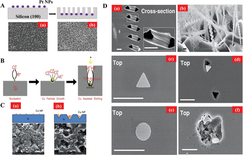
Another approach called metal assisted chemical etching (MACE) has been reported for the nanopores formation based on unique electrochemical properties of silicon wafer.[80-83] Tsujino and Matsunura reported that in HF and hydrogen peroxide (H2O2) solvent combining the function of silver particle as a catalysis, the cylindrical nanoholes were formed.[82] They also reported in 2007 that the concentration of H2O2 would affect the pore size and pore morphology also depended on the morphology of catalysis.[84] MACE is potentially efficient for manufacturing of nanopore or nanochannel structures. For example, the article described that in the 0.18 m H2O2, the Ag nanoparticles sank into the silicon and a depth of 100 nm channels were formed in 5 s, as shown in Figure 10A. Besides, the pores shape relied on the shape of Ag particles. Additionally, the etching depth and diameters of the nanopores would be expanded by increasing the concentration of H2O2.
Toan et al. reported the silicon nanopore array with 15 nm average diameter within a 200 µm thickness wafer (Figure 10B) by a dewetting method via MACE.[85] To be specific, there was one or two kinds of noble metals, such as Au, Ag, or Pt mixing in the HF/H2O2 solution dropped onto the substrate wafer. The metals went down by chemical etching so that the silicon nanopore channel formed. For its mechanism of nanopore formation by MACE, the well accepted model was oxidation-reduction reaction between Si wafer and metal particles.[86, 87] It was concluded that electrochemical potential of H2O2 was much more positive than that of valence band of Si. Thus, Si wafer could be slowly etched by in HF/H2O2 solvent.[88, 89] Wang et al. have proved that there was a spontaneous bias at the interface between metal and silicon that was appliable on both p-type and n-type silicon wafer.[90] As long as the concentration of HF/H2O2 was high enough, the etching speed would be faster which was ascribed to that the interfacial electron field at the interface between Ag particles and silicon was expanded even overlapped.
Numerous alternative metals based on the same mechanism have been reported to obtain faster etching rate and lower cost. Peng et al. fabricated nanopores with deep channels by platinum (Pt) as described in Figure 11A.[91] The Pt nanoparticles were deposited on silicon wafer (100) in the solution of HF/K2PtCl6 where silicon wafer was etching after 2 min. The nanoscale pores were formed in a relatively big area, but the pores distribution was random. Zheng et al. has reported the metal assisted chemical etching by a lower-cost copper (Cu) catalyst in HF/H2O2 solution, as illustrated in Figure 11B.[92] Similarly, Lu and Barron fabricated the pyramidal nanopore array structures on the black silicon, as illustrated in Figure 11C, where the authors additionally added 10 mm H3PO3 during chemical etching.[93] As a result, the etching rate was accelerated compared with that of no H3PO3 additive in Figure 11C(a). Besides the regular shapes, Yasuda et al. reported a helical nanopore pattern as shown in Figure 11D(a),(b). The research indicated that the diameter of helical nanopores were around 200–300 nm mostly. Besides, the author fabricated the triangular and circular nanopores exhibited as Figure 11D(c),(d) and (e),(f), respectively. It was clearly seen that the triangular pores were formed regularly. On the contrary, the circular pores were formed randomly. It is interesting that the authors have achieved complicated patterns by self-assembly MACE approach which rotated metallic Pt nanoparticles in the condition of oscillatory for the reduction of hydrogen peroxide at the interface of Si/Pt, it would promote the nanoparticle movement, then further forming helical nanopore.[94]
Chen et al. proposed a method for nanopore array formation based on self-assembly and chemical etching assisted by machine learning that determined best composition of etchant, and successfully achieved sub-10 nm in size shown in Figure 12.[44] In Figure 12A, the author developed a new method for exploration of nanopore array involving a support vector machine (SVM) algorithm that assists to optimize experimental conditions. A visualized distribution range for etching process including unetched, ideal, and over-etched diagraph is shown in Figure 12B. Based on the relationship between etching time and H2O2 volume, the etching condition can be optimized. The ideal condition for forming nanopore array based on the SVM algorithm has been established as shown in Figure 12C–G. Among them, only nanopore array morphologies conducted by the ideal algorithm results based on ML model were zoomed in and inserted in the related models, respectively. The ideal nanopore array such as the image zooming in Figure 12D has been obtained around 9 nm in diameter within 8 min etching duration. Figure 12H described the relationships between the doping concentration of Si samples and relative area of ideal nanopore structures. It is clear that the ideal regions only took up less than 5% of the entire distribution area. Moreover, the relative ideal areas for P-type Si declined faster than those of N-type Si that suggested N-type was less sensitive to the doping concentration than P-type.[44]
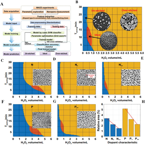
Wet etching can achieve formation of large area of nanopore array. One major advantage is that it could create high density of holes on the substrate and fabricate the nanopores with high speed. However, the wet etching is hardly to achieve the uniform distribution and regular shapes of nanopores. This disadvantage would largely produce negative effects in the applications, such as molecules detection. Fortunately, in recent years the newly developed ML probably could get over the hurdle like Chen's work in 2021 achieved the sub-10 nm nanopore array by determination of best composition. It is clear to see that ML would ease the manufacturing and prompt the efficiency which might become one of the future hotspots.
2.7 Hybrid Fabrication
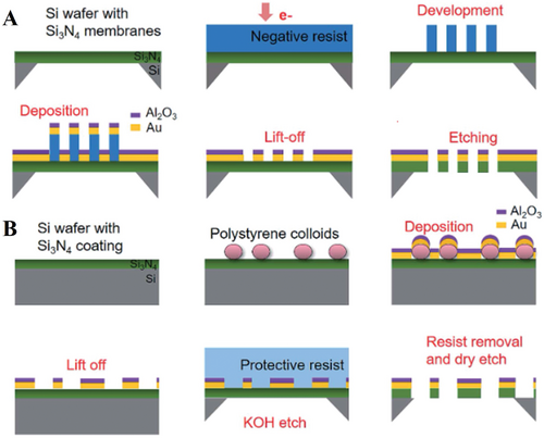
Nowadays, more and more fabrication means are being developed to achieve higher standard of nanopore crafts. Therefore, combination of various approaches is likely to bring us new possibilities. The hybrid fabrication is a well-planned and well-organized process as each step performs with a specific technical objective and their combination aims at a high-quality nanopore array structure. In other words, each step is implementing for a specific function. The hybrid fabrication of nanopore array has been reported by Malekian et al. who described the new method called colloidal lithography (CL) through polystyrene colloids and electron beam lithography (EBL), as shown in Figure 13. Figure 13A describes the process of EBL deposition for long-range nanopore channels: 1) Si3N4 was deposited on the Si membrane; 2) the negative resist was used that the metallic apertures could be formed before etching in order to avoid that the metals exist on the walls in the wafer based on the previous report; 3) nanopore array was formed via ELB; then 4) the metal Au and metallic oxide layer (Al2O3) as a protective layer were deposited by conventional electron gun heating before 5) resist lifts-off; then 6) dry etching for nanopore array.[95-97] On the other hand, the author proposed a new method, based on the report of Dahlin et al., that was polystyrene colloids assembling on the Si3N4 membrane and then lifting the colloids after depositing Au and Al2O3 layer, as illustrated in Figure 13B.[96, 97] By this improved fabrication approach, it could avoid metal residues depositing on the dielectric membrane caused by the imperfect directionality of the nanopores. The nanopore channels were formed in limited regions after chemical etching by KOH.
3 Applications of Nanopore Array
In this section, the applications of nanopore array are discussed from the aspects of DNA/RNA detection, energy conversion and storage, water desalination, nanosensors, nanoreactor, and dialysis.[2, 11-14, 25, 7, 98-103, 105-123, 127-130, 145-148, 150-159] Table 2 briefly summarizes these typical applications.
| Applications | Subareas | Nanopore/device property | Description | Refs. |
|---|---|---|---|---|
| DNA/RNA sequencing | Ultratiny pore size (≈1 [nm]) and ultrathin membrane (ideally <1 [nm]). | The ionic current will exhibit some diversity when DNA/RNA strand passes through the nanopores. By reading the current discrepancies, different nucleotides (A, G, C, T) can be identified. | [11, 25, 99, 105-109, 111-113, 115-120, 122, 123] | |
| Energy conversion and storage | Supercapacitor | Nanopore/nanoporous structure with large surface specific area. | The nanoporous/nanopore structures with super large surface specific area benefits electron transportation, enhances electron conductivity, electron charge and discharge. | [7, 127-129] |
| Water splitting | Nanopore/nanoporous structure with large surface specific area. | The nanoporous/nanopore structures with large specific area provide catalysis with larger activate sites, leading to enhanced redox reaction. | [130] | |
| Water desalination | Nanopore size matches the sizes of molecules/ions in solution. | Nanopore array (or nanopores with modifications) for water desalination have indications of high selectivity on molecules/ions types. However, most of these research are still staying in the theoretical simulation, lack of solid experimental evidence. | [101, 131, 132] | |
| Nanosensors | Molecules detection | 433 [nm] glass nanopore[137]; 230–250 [nm] glass nanopore[138]; 101 [nm] TiO2 nanopore.[139] | The nanopore (or nanopore with modifications) exhibit high selectivity in identifying specific molecules.[137, 138] Nanopore structure can also work as a 3D substrate for detection of toxic molecules by surface-enhanced Raman scattering (SERS).[139] | [137-139] |
| Optics | ≈200 [nm] nanopore on 5 [nm] thick SiN grid. | Optical enhancement or reduction as the result of optical interference. | [140] | |
| Metallic ions detection | ≈1 [nm] wide and 30 [nm] thick SiNx nanopore[141]; ≈5 [nm] nanopore.[143] | Nanopores with modifications shows high selectivity to some specific ions. | [141, 143] | |
| Nanoreactor | About 10 [nm] nanopore[145]; 30–100 [nm] [146]; 90 [nm][147]; 40–60 [nm].[148] | The nanopore works as a nanoreactor and “fume hood.”[145, 146] The oxygen molecule could pass through the nanopores and participate in the redox reaction.[147] Nanopores enhance CO2 sorption ability in gas phase and provide active sites and promote the reaction selectivity in liquid phase.[148] | [145-148] | |
| Dialysis | Artificial kidney | Bionic slit-shape nanopore[150]; round-shape nanopore[152]; layerd double oxides (LDO) structure.[153] | The function of nanopore is “ultrafiltration.” The nanoparticles selectively pass through this filter, and additionally the special structure[153] has large specific surface areas which adsorbs the uremic toxins. Nanopore filter could also act as a membrane to generate electrical energy because of the salinity gradient. | [150-153] |
| Reverse electro-dialysis (RED) | 5 [nm][157]; graphene nanopore is around ≈3 [nm][159] according to simulation.[160] | [157, 159, 160] |
3.1 DNA/RNA Sequencing
DNA/RNA sequencing based on the nanopores has been increasingly investigated due to its cost-effective, label free, long length read, and no amplification requirement that proved an exciting new tool for molecule detection.[104] Therefore, nanopore based sequencing is called the fourth-generation sequencing technique. For obtaining the best signals, the ideal condition of nanopore appliable to DNA/RNA sequencing is confined to ultrasmall pores and ultrathin membrane in several nanometers, as illustrated in Figure 14A(e),B(a). The different electrical intensities are detected when DNA/RNA fragments travel through the pore driven by a voltage, then the type of nucleotides is parsed according to these electrical discrepancies. This could also be concluded in Figure 14B(e). So far, DNA/RNA sequencing is still facing the difficulties that low ionic current and fast transportation speed (Figure 14B(c)–(e)) result in lower resolution.
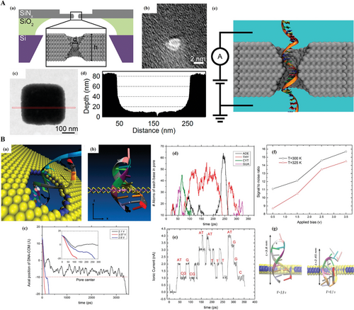
Zhang et al. proved that a smaller nanopore could would give a better resolution to the varied length of DNA.[105] Akahori et al. reported an evidence by simulation that a narrowing nanopore has the function of decreasing the translocation speed which was about 1.4 µs per base.[106] Moreover, Wanunu et al. has verified that the signal amplitude to the biomolecules was increased by declining the thickness of SiN membrane.[107] By using the blocked ionic current signal of DNA homopolymers (poly (dA), poly (dT), poly (dC)), poly (dG)), scientists have accomplished the homopolymer discrimination. The traditional substrate for the solid-state nanopores is semiconductor like SiNx with sub-2-nm diameter and thickness over 10 nm.[99, 108, 110, 111] While, the relative thick membrane would largely affect the discrimination of signals. The SiNx membrane thickness was reduced to less than 10 nm years later and greatly facilitated the RNA analysis.[107, 111-113] The smaller thickness indicates easier hydrating and better stability.[107]
In 2013, Venta et al. fabricated tiny nanopores within thin silicon nitride membranes (0.8–2 nm diameter and 5–8 nm thick membranes) through TEM drilling. The TEM image of single nanopore is shown in Figure 14A(b) and STEM images of the processed area are in Figure 14A(c),(d). The results indicated that ssDNA translocations through such nanopores largely reduced the ionic conductance by up to 70–90% which was similar to biological nanopores.[99] Lee et al. fabricated the 5 nm thickness SiNx membrane with the nanopore size of 1.5 nm for enhancing spatial resolution and largely improving signal-to-noise ratio.[109]
Besides SiNx, some other silicon-based materials were also used such as SiC, SiO2, and aluminum-based materials like Al2O3 because of their exceptional chemical, thermal and mechanical properties.[14] To be specific, the silicon-based membranes are widely used due to their low mechanical stress and high chemical stability.[14, 114] While compared to the silicon-based film, Al2O3 membrane has promoted the electrical properties with higher signal-to-noise ratio during DNA translocation.[14, 25]
Recently, the atomic-layer membranes, such as monolayer graphene and molybdenum disulfide (MoS2) membranes, bilayer boron nitride (BN), have drawn attention from the scientists due to the extraordinary electrical and mechanical performance which has the potential to replace traditional membranes.[108, 115-118] Although the high electronic signal noise and unstable detection accuracy have been improved largely by decreasing the nanopore size and optimizing the thickness of the membranes, these problems are still existing due to the high translocation speed of nucleotides (3000–5000 nt ms−1) of DNA molecules through membrane and inhibit relevant application and promotion significantly.[119, 120] Moreover, the fabrication process of nanopores usually produces undesired by-products that probably affect the nucleotides translocation.[121]
Fortunately, ML has been gaining prominently in recent years. By designing and perfecting algorithms, integrating the most key information and retraining, calculations accuracy was further prompted in order to obtain ideal nanopores. By now, researchers have indicated the positive outcomes. Liu et al. proposed recurrent neural network (RNN) which performed well on genome-scale measurement of DNA modifications.[122] Cardozo et al. achieved nanoporeTERs (or NTERs) based on the neural networks, which could measure up to nine NTERs at the same time.[123] Some other ML algorisms like convolutional neural network , SVM, learning time-series shapelets were also presented for collecting signatures from current-pulse, leading to higher detection and analysis accuracy.[124-126] Although ML assisted DNA/RNA sequencing is still in the primary stage with some obvious problems, ML indeed provides us with more possibilities in the improvement of DNA/RNA sequencing.
3.2 Energy Conversion and Storage
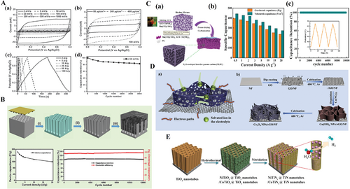
Energy conversion based on the nanoporous structures has inspired a wide range of researchers because of the superior chemical and mechanical properties, thermostability, tunable size and shape, etc.[98, 100] Compared to the traditional large-scale device, the nanomaterial energy conversion devices can supply higher energy density due to the larger specific surface area resulted from the nanoporous structures. Zhao et al. electrodeposited the Ni nanopore array based on the AAO template which provided a large specific area between the current collector and the active material.[7] Therefore, the electron-transport path was greatly shortened during the charging and dis-charging process. The promoted electron performance plots are shown in Figure 15A. Zhou et al. presented the fabrication of Co0.85Se@Ni nanopore array as hybrid electrode shown in the Figure 15B for the application of asymmetric supercapacitors.[127] An excellent performance was obtained due to the Ni nanopore array structures with a large specific surface area that greatly enhanced the efficiency of ion and electron transportation. Simultaneously, the nanopore structures could reduce the internal electrical resistance. Moreover, Wang et al. fabricated a novel material based on the nanoporous structures of carbon (Figure 15C) and Wu et al. synthesized hierarchical Co3O4 nanosheets with internal nanoporous structures (Figure 15D) which implied that the high electrical performance was ascribed to larger specific surface areas.[128, 129] In other words, the research on supercapacitors is mostly focused on nanoporous materials because the nanostructured surface provides an extremely large specific surface area and benefits ions transportation. Tang et al. synthesized the Ni-Ti and Co-Ti binary alloys, respectively, as shown in Figure 15E. Both samples have indicated the superior performance on hydrogen evolution reaction due to the large specific area leading to the high electron conductivity and fast charge transfer during electrolysis.[130] The devices consisted of nanoporous structures exhibit higher potential in applications compared to the nonporous materials, even microporous materials. Moreover, benefited from the continuous fundamental research, the miniature energy conversion devices are likely to be used as an extraordinary platform that provides an opportunity to alleviate increased energy consumption and growing pollution in energy and environment.
3.3 Water Desalination
Shortage and pollution of freshwater resources are becoming an unprecedentedly serious issue globally. Scientists have been making great efforts on working out possible solutions and measures.[103] The “U”-type device for separating heavy metal ions based on the nanopore array was invented by Liu and Zhang.[101] The “U”-type device and working mechanism are illustrated in Figure 16. The “U”-type device constitutes of feed cell and permeation cell, and the nanopore array as permeation component is polycarbonate shown in Figure 16A(c). Figure 16A(d) describes the specific detrimental ions (Cu (II), Cd (II), Pb (II), and Ba (II)) were driven by a specific voltage and the ions were separated in a certain sequence due to the selective complexation to TCAS (thiacalix[4]arene-p-tetrasulfonate).[102] In the article, the heavy metal ions separation achieved the efficiency up to 95%, 95%, 93%, 94% for Cu (II), Cd (II), Pb (II), and Ba (II), respectively in the conditions that pH equaled 5 and voltage was 1.5 V.
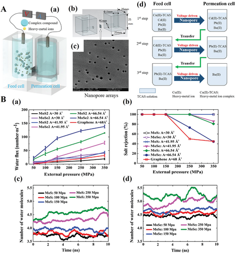
Moreover, the functional nanopore sheet has become a hotspot due to the excellent performance on filtration of water molecules. Shen et al. reported a single layer 2D MoSe2 nanopore film.[131] The simulation results show that MoSe2 nanopore can filter 10.1 L per day per MPa which has achieved nearly 2 orders of magnitude higher than commercial reverse osmosis membrane that currently widely used. The settled MoSe2 and MoS2 models with different pore sizes are compared with graphene membranes. The results indicated that both MoSe2 and MoS2 nanopore membranes overtook graphene at all given pressures on the performance in both water translocation and salt rejection, shown in Figure 16B(a),(b). Besides, the simulation also suggested that the quantity of hydrogen molecule in MoSe2 was higher than MoS2 under the same pressure. Thus, the water desalination performance of MoSe2 should be better than that of MoS2. Unfortunately, the article is only based on theoretical simulation, without experiment data for verification.
On the other hand, apart from the new generation graphene nanopores for water desalination.[132] Zhu et al. also reported a graphyne membrane which was a family of carbon allotrope and an atomic layer as graphene.[133] By simulation, the water molecules could transport through the graphyne wafer made of more than 3 sheets (n ≥ 3) as shown in Figure 17A. In Figure 17B, the simulation results suggested that when sheet number equaled to 3 or 4, the salt rejection could reach 100% at different given pressures. The cross-section view of filtration of salt and water molecules transporting through graphyne (n = 3) membrane was presented in Figure 17C,D, respectively.[133]
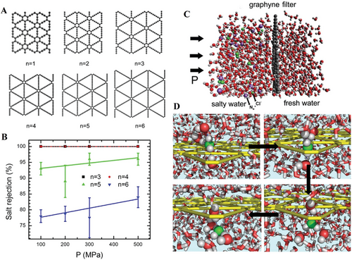
The devices based on nanopore array have already shown the superior performance on both separation of heavy metal ions and filtration of salt ions. However, it has to be mentioned that in the applicable circumstances, the situation would be more complicated for heavy metal ions separation. In other words, even though the results (Figures 16B and Figure 17) have implied the high efficiency in production of pure water, the achievable condition seems slightly stringent to the practical usage. The fundamental research of nanopore array for separation of heavy metal ions and salts from sea water are still challenging and facing many problems to be addressed for the commercialized application.
3.4 Nanosensors
Apart from detection of DNA/RNA molecules, many other molecules or particles have been successfully detected based on the diverse properties, such as the charge, molecular masses and volume, and binding with molecules, etc.[19, 20, 134-136] Holden et al. demonstrated nanopore resistive-pulse method for detecting poly N-isopropylacrylamide-co-acrylic acid (pNIPAm-AAc) microgels through glass nanopore membranes as shown in Figure 18A.[137] The microgel would be deformed when going through the nanopores, simultaneously, a pulse current would be presented. Similarly, Lan et al. presented the polymer nanoparticles detection by conical-shaped nanopores based on resistive pulse sensing theory, with similar device configuration as that shown in Figure 18A.[138] When the polymer particles transported through the nanopores, the instantaneous current would be reducing, and then recovering after nanoparticles leaving the holes.
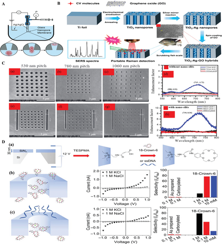
Besides, it is interesting that Zhang et al. have utilized a plasmonic 3D metallic nanopore array monitor for the application of portable surface-enhanced Raman scattering detection, as illustrated in Figure 18B.[139] The hybrid TiO2-Ag-GO nanocomposite was obtained by the method that the TiO2 nanopore array was fabricated by one-step electrochemical anodization, then Ag nanoparticles were loaded by the silver-ammonia reaction, and afterward GO thin film was coated by spin coater. Then, they used the prepared nanopore array in detecting crystal violet (CV), malachite green (MG), and thiram molecules by surface-enhanced Raman spectroscopy (SERS) which was often resided on the surface of fruits and seafood. The results suggested that the SERS curves identified the distinct intensity with different concentration of toxic molecules. It was also proved that the intensity of SERS was becoming sensitive by increasing the substance concentration and the limited detectable concentration can reach 10−10 m for CV, 10−9 for MG and 10−8 m for thiram. This plasmonic hybrid device is highly sensitive and promising for detection of organic molecules. Recently, a similar work about plasmonic nanopore array for optical enhancement was reported. Choi et al. fabricated the nanopore array platform with double nanoslits displayed on both sides. The FESEM images have shown the double slits with the pitches from 530, 780 to 1060 nm, respectively, while the diameter of nanopores is nearly 200 nm.[140] The authors explained that the optical enhancement or reduction were caused by the interference of a photonic and a plasmonic channel. Therefore, by controlling the pitch of slits, the optical enhancement was obtained as shown in Figure 18C.
Moreover, nanopore array was also applied in metallic ions detection. Acar et al. reported that the mixture of potassium ions and sodium ions selectively transported through silicon nitride nanopore membrane.[141] The nanopore inner wall was carboxylated surface made from modification of triethoxysilylpropylmaleamic acid . Then, the inner wall of nanopore was modified with 4'-aminobenzo-18-crown-6 ether on one side, and with 30-mer ssDNA on the other side, as illustrated in Figure 18D(a). Figure 18D(b) indicated that ions selectively passed through the nanopores modified with ether molecules. On the contrary, ions were prevented from transporting the nanopores modified by ether and ssDNA, as shown in Figure 18D(c). It was suggested that the molecule of ssDNA played a role of cation filter, and the molecules of crown ether played a role of selection of potassium.[142]
Furthermore, Jágerszki et al. used the synthetic nanopores for silver ions detection.[143] In the article, gold nanopore array was fabricated by electroless plating on the polycarbonate membranes, then functionalized by the mixture of Ag+-selective thiacalixarene derivative bearing dithiolane moieties, mercaptodecanesulfonate, and perfluorinated thiol derivative (SS-Ag-II/MDSA/PFT). The analysis indicated that MDSA played as cation-exchange sites. PFT increased the hydrophobicity to the Au nanopores, and PFT functioned for the potentiometric response and ion selectivity, while SS-Ag-II acted for recognition of silver ions.[143]
Besides the above applications in in-suit detection of polymers, detection of toxic substances, screening of specific ions, and optical property enhancement, there are still numerous types of nanopore sensors and devices which have superior performance to support diversified applications potentially but cannot be exhausted in this article. It is reasonable to foresee a prospect of nanopore sensors being implemented in more industrial sectors in future driven by the mature of manufacturing technologies.
3.5 Nanoreactors
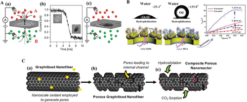
Nanopores offer a unique chemical environment partitioned from surroundings that could not only accelerate the reaction speed but also obtain insightful understanding of new reaction systems or new nanoparticles or even develop a novel analytic tool upon this “nanoreactor.”[144] For example, Venta et al. reported that the sub-10 nm diameter SiNx nanopore could be a spot where gold particles were formed under a controlled and monitored manner simply by electrical field.[145] As Figure 19A exhibits, a certain concentration of gold chloride (HAuCl4) solution in Chamber B and hydrazine solution in Chamber A were both driven into the pore direction by a voltage, then the golden particles were formed in the channel until the entire pores were filled of golden particles. Besides, the different sizes of golden particles were controlled by varying the concentration of gold chloride. Similarly, Zalineeva et al. synthesized self-supported porous PbxBi nanostructures which have large surface areas (75–100 m2 g−1). The morphology of porous nanostructures consist of beads of aggregated 5 nm nanoparticle delimiting of 30–100 nm nanopores in diameter. These nanopores form nanoreactors where reactants, intermediates, and products are confined to realize glycerol electrooxidation, and then further responsible for the selectivity of PbxBi.[146] Mi et al. reported that porous anodic alumina nanochannel structure modified by molecules could handle the challenge that low solubility would hinder the reaction which involves gases.[147] It is interesting to observe that oxygen molecules could transport to the fabricated nanochannel and reach the active sites and participate in the reaction of glucose oxidase (GOx). The schematic representation is shown in Figure 19B. The results indicated that the efficiency was improved up to 80 times in the gas–solid–liquid interfaces compared to the enzyme reaction in the pure solution. Recently, Astle et al. also reported the nanoscale confinement of the nanoparticles for enhancement of catalytic reaction.[148] To be specific, the authors adopted the chromium oxide (Cr2O3) particles to fabricate the defects that formed 40–60 nm nanopores in the walls of the carbon nanotubes . The schematic diagram is shown in Figure 19C. These porous nanotubes could act as nanoreactors and lead two catalytic reactions in gas-phase and liquid phase, respectively. In the former reaction, the simulation postulated that sorption of CO2 on Ru particles in this nanoreactor is stronger than that on amorphous carbon which indicated a novel way of bonding metal atoms.[148] Moreover, in the liquid phase where alkyne hydrosilylation reacted with Rh4(CO)12, the nanoreactors provided spots for aromatic reactant with a higher concentration around Rh active sites and promoted the selectivity.[148]
3.6 Dialysis
Recently, Tang et al. introduced an interesting topic in their review paper on successful application of dialysis: the artificial kidney.[149] Unfortunately, even though the artificial kidney is a promising “alteration” for the renal therapy to the patients, it will not become a replacement to the natural kidney due to various limitations such as the unachieved metabolic function, biological incompatibility, and complications to the patients.[149]
The filtration as one of the major functions of the artificial kidney is essential to the blood purification. Nanopore is one of the most efficient structures to support the purification treatment. However, the morphology of nanopores in this session is different from those of other applications because bionic kidney is designed to be a slit aiming at higher hydraulic permeability, so actually it is a nanoslit.[150, 151] The slit shape nanopore with surface modification by polyethylene glycol has been reported for the function of protein fouling elimination and contact activation on the silicon-based membranes.[150, 151] Fissell et al. first published the slit-nanopore (Figure 20A) that was for prolonged hemofiltration and 90 h experiment evidenced the retained hydraulic permeability and molecular selectivity.[150] This result proved the possibility of long duration renal replacement therapy. On the contrary, Yunus et al. fabricated nonslit shape nanopores ranging from 50 to 80 nm based on electrochemical etching process. These inverted-trapezoid-shaped nanopores are embedded in silicon ultrafiltration membrane where dielectrophoresis (DEP) electrodes are also fabricated.[152] Some different particles like albumin, antidiuretic hormone (ADH), blood plasma components with various sizes were tested in this “artificial kidney.” The results indicated that the particles larger than 80 nm cannot penetrate through the porous membrane. And DEP would benefit the concentration of particles as the percentage of albumin, ADH and blood plasma passing through were 65.80%, 92.60%, and 71.40%, respectively compared to 44.38%, 47.04%, and 34.08% without DEP electrodes.[152] It is suggested that ultrafiltration membrane with DEP electrodes could be one of candidates to the wearable mini devices.
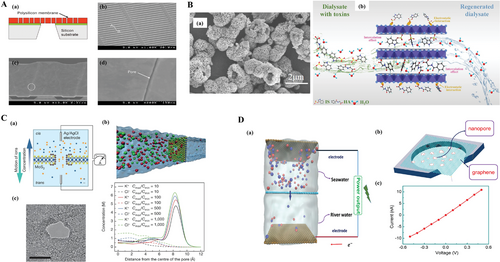
It is also reported in 2022, Ding and colleagues synthesized the MgAl layered double oxides (LDO) hierarchical structure by hydrothermal reaction and reached ultrahigh specific surface area (187.3 m2 g−1) and partitioned nanopores whose FE-SEM morphology image could be found in Figure 20B(a).[153] In this paper, the particles were then used in removing uremic toxins (HA and IS). The maximum removal rate could achieve 129.8 and 63.1 mg g–1 respectively. The working schematic plot is shown as Figure 20B(b), which generally follows kinetic adsorption principle, that means, the toxic molecules of HA and IS are adsorbed by electrostatic function. This work implies an extraordinary bulk material with ultrahigh absorption capability, which inspires us that the nanoparticles with ultrahigh specific surface area would potentially facilitate a hemodialysis device for uremic patients.
Reverse electro-dialysis (RED) is also an attractive concept which relies on the mechanism that a current is generated by mixing two solutions with distinct salinity concentrations through a cation/anion-exchange membrane.[154-156] The representative work presented by Feng et al., in Nature demonstrated a RED device with MoS2 nanopores.[157] The morphology of the MoS2 nanopore can be found in Figure 20C(c). The working schematic illustration is shown in Figure 20C(a). The 0.65 nm thick single layer of MoS2 nanopore is negatively charged, forming a screen that leads to osmotic flux toward the equilibrium state. It is interesting to see the selectivity on potassium ions and chloride ions, that molecular dynamics simulation exhibits the potassium ions is more likely to pass through the center of nanopore compared to the chloride ions, as illustrated in Figure 20C(b). Moreover, the author expanded this osmotic generator to self-powered nanosystem because of its high efficiency and power density. This RED device is also applicable to some other application fields, such as water desalination and supercapacitor for energy storage, due to the fact that such nanopore-based materials normally possess large specific surface area. Besides, Laucirica et al. reported the osmotic current could be affected by the shape of nanopores, pH value, concentration of gradient, type of salt, etc.[158] Fu et al. reported a new RED application named graphene reverse electrodialysis (GRED).[159] The layer of ultrafiltration consists of nanoporous graphene membrane on the 12 µm thick PET foil as a supporter with around 1.5 µm2 shown in Figure 20D(b). The graphene nanopores are around 3 nm in diameter according to the molecular dynamic simulation.[160] The schematic illustration of GRED working mechanism is shown in Figure 20D(a), converting salinity gradient to electrical energy. The cations pass through the graphene sheet selectively which leads to a certain current output. The electrical conversion performance of READ device was measured in 1 m KCl electrolyte and results of the voltage as the function of current are shown in Figure 20D(c). This work achieved high output energy density of 126 W m−2 and a high energy conversion of 39%.[159]
4 New Development of Fabrication of Large Area Solid State Nanopore Array
It is clarified the hybrid manufacturing process may become a possible approach for cost-effective manufacturing of nanopore array addressing some specific applications. It is believed that there is an urgent need to develop the scalable manufacturing technology for supporting potential industrial practice. The authors of this review have developed an efficient method that combines nanospheres self-assembly, fast deposition, and ultrasound-chemical assisted removal which evidenced rather competitive advantages in forming large area solid-state nanopore array. Figure 21 (top part) illustrates the key steps of the manufacturing process chain.
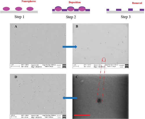
Figure 21A is the SEM image of nanospheres distributed by spin coating on the substrate surface after that 4 nm thickness Pt film was deposited through sputtering coating device. The density of the nanospheres is controllable to form the desired distribution pattern on the substrate. There are two functions associated with the thin Pt film. One works as a conduction layer for SEM measurement, the other is as deposition layer for the nanopore array formation in the next step. Then the samples were immersed in toluene liquid, with assistance of ultrasound to remove the PS nanospheres. By 5 min ultrasound, some nanopores appeared as seen in Figure 21B, with dimension around 20 nm as zoom-in in Figure 21C. Figure 21D is the SEM image after 15 min consecutive ultrasound, which indicated that more PS nanospheres were removed and consequently all nanopores were exposed. It was found that these nanopores achieved uniform shapes and sizes (20 nm round holes), and the nanopore array was formed in a large area (15 × 15 mm2), and the pore densities in several randomly selected areas are nearly the same. Moreover, experiments are being conducted to shrink the nanopore size down to 1 nm or less by controllable thermal radiation, usually within 5–10 min. This proposed process chain makes the efficiency and cost rather competitive. More details will be revealed in our later publications.
5 Conclusions and Prospects
In this review, some typical methods for fabricating single nanopore and nanopore array have been summarized, such as ion beam lithography, plasma-assisted deposition, electrochemical deposition, electrodeposition, electrochemical anodization, and wet etching. Moreover, some unconventional ways for manufacturing nanopore array are also included to indicate new possibilities, like the nanobubble-based electrodeposition and machine learning assisted chemical etching. Although in theory the techniques valid for single nanopore should be potentially applicable to the fabrication of nanopore array, nanopore array presents more stringent challenges practically to the manufacturing technologies which results in low fabrication efficiency, nonuniform shape, poor size repeatability, irregular (uncontrollable) distribution pattern, and high production cost. Therefore, ultraprecision manufacturing of nanopore array is still a global challenge as well as a key technique for industrial practice in consideration of short of cost-effective manufacturing process chains. To conquer this barrier, conventional research routes need to vary which usually focus on a small quantity of nanopores (including single nanopore) and production cost tends to be overlooked. This was evidenced by the limited outputs (and publications) on large area nanopore fabrication, and lack of spotlighting the manufacturing efficiency or manufacturing cost with convincing details.
The hybrid manufacturing method emerges with significant advantages for fabricating nanopore array. The combination of selected processing techniques offers more flexibility on controlling the nanopore size and distribution pattern and optimizing the process parameters for improved manufacturing efficiency and lowered cost. The authors of this review successfully used a low-cost hybrid process to fabricate 20 nm nanopore array in a 15 × 15 mm2 area, with relatively uniform pore shape and size. The experiments also indicated a possible way to reduce the pore size down to 1 nm simultaneously modify the geometry of nanopore channel, which would be a breakthrough to facilitate the high-resolution DNA sequencing. As the ideal pore geometry for DNA sequencing would be 1 nm in diameter and below 0.5 nm in channel length, this is quite a challenge for conventional nanomanufacturing methods. But using hybrid method, it is possible to separate the key requirements and choose the most suitable (and efficient) technology for each, e.g., using molecular self-assembly to form a template for controlling the nanopore distribution and basic shape, and then using shrinkage technology to reach the expected pore size and modify the geometry of pore channel. Definitely we could have more technology combinations for such hybrid methods, especially in future the technological progressing would enable more options.
Besides, machining learning also provided preliminary experimental evidence on its capability of improving the nanopore fabrication efficiency, seeing the achievement of 9 nm nanopore array within 8 min etching duration. Although such method is still in the fledging stage and has not been applied for large area nanopore array, we cannot ignore the sign that emerging technologies can bring us some unexpected surprise. Not only the machine learning, but the researchers could also extend their vision to more diversified disciplines.
Furthermore, these nanopore manufacturing technologies have indicated great potential in fabricating nanoscale 3D functional structures, thus possibly become the effective approaches for the atomic and close-to-atomic scale manufacturing (ACSM), which is the fundamental technology of the new manufacturing advancement paradigm, namely Manufacturing III.[161-163]
So far, there are few commercialized solid state nanopore sensors available in the market which significantly limits its uptake in industrial applications although its extraordinary properties have been verified through extensive lab research. The major bottleneck is lack of cost-effective and efficient manufacturing process chain. However, as introduced in this paper, a variety of potential applications based on solid state nanopore (array) have been investigated in labs, addressing various industrial sectors, which indeed foresees the promising prospect of this tiny sensor in future. It is also encouraging to see researchers are seeking for more competent manufacturing methods to improve the quality of solid state nanopore sensors, along with higher efficiency. If the manufacturing barrier could be conquered, definitely we have the reason to believe solid state nanopore array could bring significant changes to both our daily life and industrial production by enabling more powerful devices.
Acknowledgements
This publication has emanated from research supported in part by a grant from Science Foundation Ireland under Grant No. 15/RP/B3208. For the purpose of Open Access, the author has applied a CC BY public copyright license to any Author Accepted Manuscript version arising from the submission. The authors would like to thank the “111” Project by the State Administration of Foreign Experts Affairs and the Ministry of Education of China (No. B07014). [Correction added after publication 8 February 2023: Fig. 1 was updated.]
Open access funding provided by IReL.
Conflict of Interest
The authors declare no conflict of interest.
Biographies

Hongshuai Liu is a Ph.D. candidate in University College Dublin (UCD), Ireland. He received B.Sc. degree in Physical Materials in Lanzhou University in 2015 and M.Sc. degree in Material Science in Shandong University in 2018. He worked as the research assistant in Hong Kong Baptist University (HKBU) between 2020 and 2021. His current research focuses on nanopore array fabrication and improvement for DNA sequencing. By now, he has successfully fabricated large area of solid state nanopore array with <20 nm diameter using a cost-effective hybrid method.

Qin Zhou is a top-two level tenured professor and the Vice President of Harbin Medical University, China. Prof. Zhou devoted himself to the field of laboratory medicine, instant screening test (IST) and protein ubiquitination. Prof. Zhou obtained his M.D. and Ph.D. from Fudan University and worked as a postdoc at Johns Hopkins University. He was the director of the Key Laboratory of the Ministry of Education. Prof. Zhou has published over 60 peer-reviewed research articles in international journals including Nature Communications and Biomaterials.

Wei Wang, Professor, University of Electronic Science and Technology of China. Prof. Wang obtained his bachelor degree from Wuhan University in 2002 and the Ph.D. degree in Harbin Institute of Technology in 2010. He worked as a post-doctoral fellow in the S. M. Wu Center of University of Michigan, Ann Arbor. He is now working on ultraprecision manufacturing and ultraprecision measurement. He has published over 30 papers including the Journal of Machine Tools and Manufacturing, Mechanical System and Signal Processing. Now he serves as a member of ISO TC39/SC2 committee and contributes to the ISO standard 10791-7, ISO 10791-6.

Fengzhou Fang is a joint professor working at University College Dublin in Ireland and Tianjin University in China, and the director of Centre of Micro/Nano Manufacturing Technology. He is the Fellow of ISNM, Fellow of AET, Fellow of CIRP, and Fellow of SME. His research interests include fundamental studies and application development in the areas of nanomanufacturing, atomic and close-to-atomic manufacturing, optical freeform design and manufacturing, ultraprecision machining and measurement. Prof. Fang is the Editor-in-Chief of Nanomanufacturing and Metrology.

Jufan Zhang, assistant professor & lecturer in UCD School of Mechanical and Materials Engineering, faculty member of UCD Centre of Micro/Nano Manufacturing Technology, Ireland. He is leading the research in manufacturing of solid state nanopore array and corresponding biomedical applications by collaborating with academic and industrial partners. He has chaired 14 research funding, and made 50 peer-reviewed publications and 7 patents on nanomanufacturing, ultraprecision machining, biomedical devices and optics. He has given over 10 keynote/invited talks in the recent one year on nanomanufacturing and biomedical research.


