Demonstration and Evaluation of p-Type and n-Type ZnO Nanoparticles-Based Homojunction UV Light-Emitting Diodes
Abstract
The world's first homojunction UV light-emitting diode (LED) based on both p-type and n-type ZnO nanoparticles (NPs) is demonstrated. Nitrogen-doped ZnO and gallium-doped ZnO NPs are provided to fabricate p-type and n-type NP layers, respectively. The LEDs with the structures of p-ZnO/GZO and p-ZnO/n-ZnO/GZO are fabricated. These devices show near UV electroluminescence (EL) at room temperature and emission power doubled by inserting the n-ZnO NP layer. By comparing the results of I–V, EL and photoluminescence for LEDs, it can be confirmed that the holes inject from p-ZnO NP layer to n-ZnO NP layer and the mechanism of these devices are that of p-n junction LEDs.
1 Introduction
In the illumination technology era, light-emitting diodes (LEDs) have vast potential use in solid-state lighting for their high efficiency, low power consumption, low heat output, and long lifetime. Currently, gallium nitride (GaN) based LEDs have been widely applied for various applications such as lighting and display due to their improvement of luminescence efficiency.[ 1, 2 ] However, they have a cost issue because all the commercial LEDs are fabricated by an expensive single crystal-based semiconductor process.
As a favorable material for future applications of LED, zinc oxide (ZnO) has exciton binding energy of 60 meV, direct wide bandgap and a short wavelength light emitting region from blue to near-ultraviolet at or even above room temperature.[ 3, 4 ] Also, it can be fabricated relatively inexpensively compared to other III-V semiconductors. In order to realize ZnO-based LEDs, the major challenge is the production of high-quality p-type ZnO. Group V elements (N, P, As, and Sb) are the most reliable dopants for p-type ZnO. Recently, ZnO-based LEDs were fabricated using nitrogen-doped ZnO or MgZnO with single crystal films.[ 5-7 ]
The device fabrication using nanoparticles (NPs) is a unique and cost-effective technique. Nitrogen (N)-doped ZnO NPs were researched by several groups using various fabrication methods.[ 8-10 ] Our lab group synthesized N-doped ZnO NPs by using a gas evaporation method.[ 11, 12 ] These particles have the possibility to act as a p-type semiconductor. TFT and near UV LEDs were demonstrated[ 13, 14 ] by using N-doped ZnO NPs for the p-type layer. This NP-based process does not need single-crystal substrate which has the potential to realize low-cost semiconductor devices. Most of the device making process can be done in the atmosphere and does not require a vacuum state. Another advantage is that it can be possible to accomplish a large or small surface emission area and reduce the heat problem of the LEDs. Although the electroluminescence (EL) was dominated by defect emission, Neshataeva et al.[ 15 ] demonstrated large area heterostructure LED based on ZnO NP by simple coating process. Fujita et al.[ 14 ] had reported the structure and optical properties of p-ZnO NPs-based LED coated on Ga-doped ZnO (GZO) transparent electrode films and demonstrated the near ultraviolet EL. However, EL was observed only from the p-type layer because GZO has very weak luminescence and had been used for the n-type layer.
In this research, we constructed ZnO NPs based on homojunction LEDs by N-doped p-type and Ga-doped n-type ZnO NPs. The p-type and n-type NP layers were created on GZO electrode films by simple coating methods.
2 Results and Discussion
In our ZnO NPs, nitrogen was chosen as a p-type dopant because it has a similar ionic radius to oxygen. The nitrogen incorporation and concentration were dependent on arc current and chamber pressure. The details are described in our previous research articles.[ 11-14 ] Two different conditions were used in the prospecting of achieving p-type ZnO and n-type ZnO NPs. We followed the condition with an arc current of 30 A and chamber pressure of 150 Torr to synthesize ZnO NPs with high nitrogen concentration (≈2.6 × 1019 cm−3) which were used to make a p-type layer in the diode. Low nitrogen concentration (around 7.7 × 1018 cm−3) ZnO NPs were prepared and used for Ga doping at the arc current of 70 A and chamber pressure of 610 Torr.
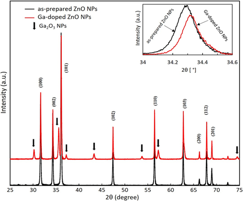
Group III element, Ga was used for an n-type dopant, which can easily substitute Zn site and acts as shallow donor in ZnO. Ga doped ZnO NPs are prepared by thermal diffusion of Ga into ZnO using Ga2O3 NPs as a diffusion source. Figure 1 expresses the X-ray diffraction (XRD) of the powder samples as-prepared ZnO NPs (chamber pressure of 610 Torr and arc current of 70 A) and Ga-doped ZnO NPs. The diffraction peak of the as-prepared NPs and Ga-doped NPs have a well-described hexagonal wurtzite structure with exact orientation which is in agreement with the standard JCPDS data (card no. 36-1451)[ 16 ] for ZnO. Some additional peaks corresponded to Ga2O3 in addition of Ga-doped ZnO NPs. The (002) diffraction peak (34.29°) for as-prepared ZnO NPs showed lower angular position compared to that of bulk ZnO (34.42°)[ 17 ] because of the variation in the lattice constant of nitrogen containing ZnO NPs. In Figure 1, the right side inset show the enlarged view of the XRD (002) peaks. It shows that the observed (002) diffraction peak (34.326°) of Ga-doped ZnO NPs is a slightly higher angle compared to the as-prepared ZnO NPs peak position (34.29°). The reason is that the lattice constant c (Å) of the Ga-doped ZnO NPs changed. The lattice constant decreased owing to the introduction of a foreign impurity (Ga doping) in the host ZnO lattice. This is the main outcome due to the size difference of ionic radius Zn (0.60 Å) and Ga (0.47 Å).[ 18 ] The phenomenon is due to the ZnO lattice distortion, which is induced by the small size of the Ga atom and decreases the lattice constant. Gomez et al.[ 18 ] expressed that the reducing lattice constant (c) depends on the increasing Ga content in the ZnO lattice.
We conducted the PL measurements of ZnO NPs sprayed layer on the substrate. Figure 2 indicates the PL spectra of as-prepared ZnO NPs, Ga-doped ZnO NPs, and N-doped ZnO NPs layers. Note that we used weak lamp source to emphasize the defect emission by weak excitation condition. From the PL spectra, a sharp and dominant UV emission around 380 nm was detected, corresponding to the ZnO near band edge (NBE) transition. A broad deep-level emission is attributed to the point defect-related transition of ZnO NPs.[ 19 ] The deep-level emission is caused by point defects like vacancies (V Zn, V O) and interstitials (Zni). The comparison of PL spectra refers to relatively improved NBE PL intensity in Ga-doped ZnO NPs because Ga behaves as an activated donor and generated charge carriers.[ 20-23 ] The defect level emission of Ga-doped ZnO NPs showed significant reduction owing to diffused Ga and O into the vacant site in ZnO. The above discussion on PL spectra has indicated that these Ga-doped ZnO NPs have comparatively low defects and are applicable for the n-type layer of LEDs.
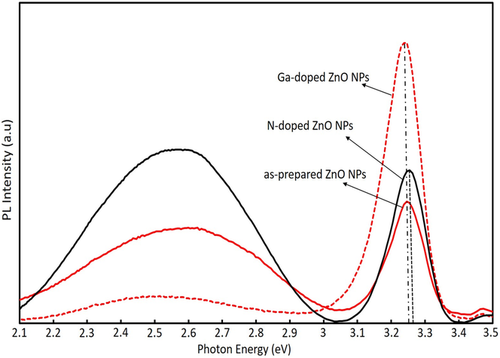
Figure 2 also shows the comparison of PL spectra that the near band edge (NBE) emission peak energy (3.246 eV) for the Ga-doped ZnO NPs layer was shifted compared to those for the N-doped ZnO NPs layer (3.263 eV). The reason for the redshift is probably due to the increase of electron concentration and arising donor–acceptor pair transition[ 24 ] in addition to the excitonic emission.
We conducted the Hall measurement of the N-doped and Ga-doped ZnO NPs films. The mobility of N doped films was about 4.61 cm2/Vs and those of Ga-doped were 6.63 cm2/Vs. The carrier concentration of the N-doped ZnO NPs films and Ga-doped ZnO NPs films were about 3.2 × 1013 cm−3(p-type) and −2.696 × 1014 cm−3(n-type), respectively. However, these results were dominated by the property of so many boundaries between NPs.[ 13 ] This is different from the case of LEDs because the current of LEDs flow in a direction perpendicular to the film surface and the number of boundaries is small. But hereinafter, we denote N-doped ZnO as p-ZnO and Ga doped ZnO as n-ZnO.
A cross-sectional view of the LEDs with a different structure is indicated in Figure 3a,b. One is the p-ZnO NP layer on the GZO electrode and another one is p-ZnO NP layer and n-ZnO NP layers on GZO respectively. We cut the samples with a diamond wire cutter for viewing the cross-section of the device layers. The samples were not cut precisely due to the NP layer during the cutting process. But it could be estimated that the thickness of spin-coating p-ZnO NP layer was around 3 μm and that of the sprayed n-ZnO NP layer was about 2 μm.
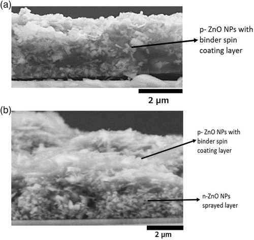
The average size of ZnO NPs was about 150 nm as reported in our previous research.[ 25 ] For the spray coating process, we used n-ZnO NPs dispersions. The Sprayed NPs were sintered before aggregation occurred to make a denser NPs film by using a hot plate during the spray process. On the contrary, aggregation of the p-ZnO NPs is needed for the spin coating layer to get the current pass in the insulating binder.
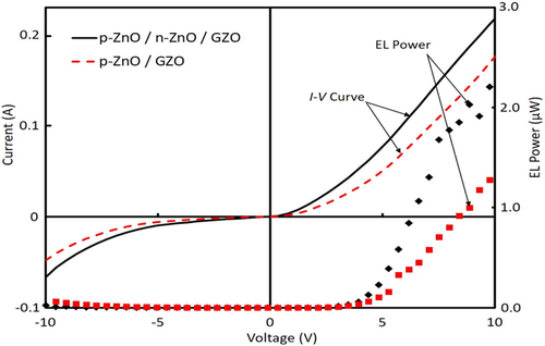
Here, Ωc = 2π (1 − cos θ c); critical angle, θ c = sin−1(1/n).
The total EL power is roughly estimated to be about 12 times larger than the measured value only assuming the total reflection of the glass substrate surface. The EL power for p-ZnO/n-ZnO/GZO LED shows the droop effect at a higher voltage region, probably due to the higher current density of p-ZnO layer so that the current pass was constricted by the insulating binder and heating of the device by the higher input power. It shows about two times larger than that of p-ZnO/GZO LED at the voltage under the drooping area.
Figure 5 displays the comparison of EL spectra for ZnO NPs based LEDs. The EL spectrum intensity was enhanced remarkably by inserting the n-ZnO NPs active layer compared to that of without n-ZnO NP layer. In these LEDs, GZO layers did not act as a luminescence layer because GZO electrode film has a very high electron concentration (≈1021 cm−3) and weak luminescence, where the n-type GZO electrode layer rolled as a current spreading layer to increase the uniformity of electron injection. In the structure of p-ZnO/GZO LEDs, the carrier recombination occurred in the p-ZnO NP layer by electron injection from GZO because the active area exists only in this layer. On the other hand, the structure of p-ZnO/n-ZnO/GZO LEDs, n-type ZnO NP layer had low carrier concentration compared to GZO. The charge recombination would be produced in the n-ZnO NP layer which worked as an active region. Thus, the enhancement of EL is due to the addition of the n-type layer and this layer was acting as a light-emitting layer. In that case, hole injection should occur from the p-ZnO layer to the n-ZnO layer.
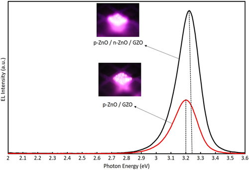
The EL emission peak energy for p-ZnO/GZO LED was found at around 3.20 eV and the EL peak energy for the device adding an n-ZnO layer (p-ZnO/n-ZnO/GZO) was observed near 3.23 eV as displayed in Figure 5. Both of the EL peak energies were shifted to the lower energy side compared to the PL spectra as shown in Figure 2. On the other hand, the EL peak of p-ZnO/n-ZnO/GZO showed higher energy than that of p-ZnO/GZO that is the opposite of the PL result. One of the reasons for energy shift to the lower direction is considered to be a reduction of the bandgap energy by the temperature rise.[ 27 ] If this is the main reason, p-ZnO/n-ZnO/GZO LED should have a larger shift because it observed a droop effect in the EL emission power, but the result is inconsistent. Another possible reason is red-shifts by exciton-exciton collision and electron–hole plasma at a higher injected carrier concentration in the device, which is similar to those observed in PL spectra at a higher excitation density.[ 28, 29 ] Assuming this effect is consistent with the experimental result because the carrier flow pass in p-ZnO layer with a binder will concentrate in the NPs in an insulating binder resulting in higher excitation density and a large red shift as presented for p-ZnO/GZO LEDs in our previous report.[ 14 ] However, the carrier flow pass in the n-ZnO layer will spread to the NP layer without a binder, resulting in lower excitation density and smaller red shift. The EL emission of p-ZnO/n-ZnO/GZO LEDs was also measured at the injection current of 40 and 200 mA. The EL peak position at the low injected current of 40 mA was 3.243 eV, that was almost same as the PL peak energy (3.246 eV) of Ga-doped n-ZnO NPs layer and the EL peak position at 200 mA was 3.230 eV. It is also consistent that the red shift by D–A pair emission and defect emission observed in PL spectra excited by weak lamp source, which were not observed in EL spectra because of the intensities of these emissions, will saturate at such a strong excitation condition as these transitions are limited by the density of the levels, unlike excitonic emission. Thus, we can consider that the detected EL emission of p-ZnO/n-ZnO/GZO LEDs was attributed to the radiative recombination in the n-ZnO NP layer as well as p-ZnO layer.
3 Conclusions
We attained fabrication of light-emitting devices by using N-doped p-type and Ga-doped n-type ZnO NPs according to facile and manageable methods. By considering the overall results including electrical and spectral evaluations, it can be concluded that the hole injection from p-ZnO NP layer to the n-ZnO NP layer occurred and the mechanism of these LEDs are p–n junction based. This is the first demonstration of p-type and n-type ZnO NPs-based homojunction LEDs. Though the output power is still impractical, it will be possible to realize the low-cost NP based semiconductor devices as well as light-emitting devices by improving performance.
4 Experimental Section
We prepared N-doped ZnO NPs by a zinc-metal vapor technique (ULVAC Inc. Model No- GE-970) with the radicals (oxygen and nitrogen) created in the air plasma. The detailed experiment and mechanism were presented in our previous report.[ 11 ] In the experiment, zinc metal (Nilaco corporation—Zn 99.99%) was used as a zinc source and dry air with 5 L min−1 flow rate was applied as the oxygen and nitrogen source. A simple oxidation process was induced by an arc current at 20–70 A between a carbon cathode and a metal zinc source. The chamber pressure was regulated at 150 and 610 Torr by the regulating valve and the rotary pump throughout the generating period.
Ga doped ZnO NPs are prepared by thermal diffusion of Ga into ZnO. In this case, 0.1 g as-prepared ZnO NPs (Synthesized at the chamber pressure of 610 Torr and arc current of 70 A) and 0.015 g of Ga2O3 particles (Sigma Aldrich Co. Ltd.), as a Ga source, were mixed in the crucible and annealed under N2 flow (0.5 L min−1) in atmospheric pressure for 60 min. The temperature was increase from room temperature to 900 °C within 10 min, and after 60 min thermal treatment, the samples were cooled down to less than 40 °C in 2 h. The detailed experimental procedures were discussed in the research article.[ 25 ]
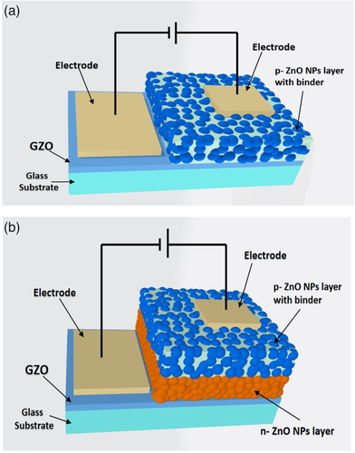
We designed two types of ZnO NPs LEDs. One type of LED had a N-doped p-ZnO NP layer on the GZO (Ga-doped ZnO) transparent conductive film and another type had a N-doped p-ZnO NP layer and a Ga-doped n-ZnO NP layer on the GZO film as displayed in Figure 6a,b respectively. The GZO films (thickness of 500 nm) were deposited by RF magnetron sputtering (Canon Anelva Corporation, Model- 400S) at 300 °C using 5% Ga doped ZnO target on the white glass substrates (thickness of 500 μm). The n-ZnO NP dispersions were prepared by mixing 20 g pure water with 0.2 g Ga-doped ZnO NPs using an ultrasonic homogenizer. The large size particles were separated from the dispersion by a centrifugal separator (Kubota Laboratory Centrifuges Japan, Model- RA-2724) (3000 G, 1 min). For the formation of the n-ZnO NP layer, the separated dispersion (3 mL) was sprayed using an airbrush spray process at 5 s intervals for ≈7 min onto the GZO electrode film which was on the hot plate at the temperature of ≈300 °C.
The synthesized p-type ZnO NPs (0.05 g) were mixed with isopropyl alcohol (IPA) (0.3 mL) and (0.1 g) binder (Silsesquioxane OX-SQ ME 20, Toagosei Co., Ltd). This mixture was coated on the GZO and/or n-ZnO NP layer for the fabrication of LEDs. The spin coating condition was maintained at an initial speed of 1000 rpm for 5 s and accelerated to a speed of 4000 rpm for 10 s. The coated NP layer was sintered on the hot plate at ≈300 °C for 1 min. Finally, gold (Au) was deposited as a contact electrode with 30 nm thickness on both the p-ZnO NP layer (1 mm square) and transparent GZO film (large shape) by the vacuum deposition. The ohmic characteristic between the gold (Au) electrode and p-ZnO NPs film was confirmed (The I–V curve is presented in our previous article[ 13 ]).
The nitrogen concentration of ZnO NPs was measured using Horiba EMGA- 830 for analysis of nitrogen. The XRD of the NPs samples was measured by a diffractometer (Smart Lab Rigaku Corporation) with Cu Kα radiation. Horiba FluoroMax-4 Spectrofluorometer was used to observe the photoluminescence (PL) spectra with an excitation wavelength of 325 nm using a Xe lamp with a monochromator. A scanning electron microscope (JEOL Ltd., JCM-7000) was used to study the cross-sectional image of the ZnO NP layer. The I–V characteristics and EL power measurement of LEDs were carried out by using a parameter analyzer (B2900A series of High-Resolution SMU module, Keysight Technologies) and Si photodiode (S2281, Hamamatsu Photonics), respectively. EL power emission was measured from the glass substrate side. Ocean Optics QE65000 fiber multichannel monochrome meter was used to evaluate the EL spectrum from the p-contact electrode upside at room temperature.
Acknowledgements
This work was partially supported by MEXT of Japan City Area Program of Shinji Lake & Nakaumi (2009-2012), JSPS KAKENHI grant number 25630150, The Canon Foundation and S-Nanotech Co-Creation Co., Ltd.
Conflict of Interest
The authors declare no conflict of interest.
Open Research
Data Availability Statement
The data that support the findings of this study are available on request from the corresponding author. The data are not publicly available due to privacy or ethical restrictions.


