Bottom-up assembly of nano-carbon devices by dielectrophoresis (Phys. Status Solidi B 12/2013)
Graphical Abstract
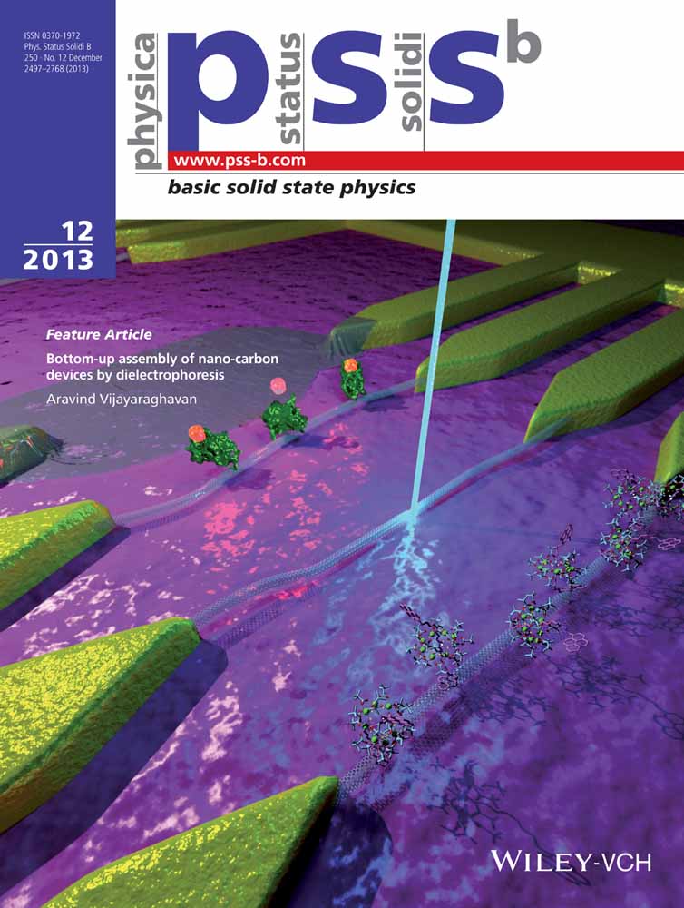
In the past decade, an unconventional approach to large-scale fabrication of carbon-nanotube and graphene devices has emerged, namely, dielectrophoretic (DEP) assembly. This technique has now been demonstrated in wafer-scale assembly of nano-carbon electronic devices, sensors, opto-electronic devices and even suspended structures. It has also served as an enabling tool for a number of experiments which might otherwise not be possible. A detailed review of developments in DEP assembly of nano-carbons is presented as a Feature Article by Aravind Vijayaraghavan (pp. 2505–2517). The cover image is an artist's concept of some typical carbon-nanotube and graphene devices assembled by DEP (image courtesy N. Clark).