Halide Chemistry in Tin Perovskite Optoelectronics: Bottlenecks and Opportunities
Graphical Abstract
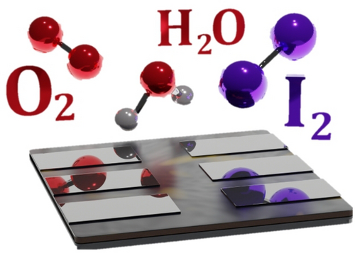
Efforts to boost tin halide perovskite optoelectronics have focused heavily on the instability of SnII, while other inconspicuous chemical processes have remained unexplored. This Minireview highlights the key role of native halide chemistry in the stability, device performance, ecological impact and prospects for visible light emission in this class of materials. Halide management routes towards viable optoelectronics are also proposed.
Abstract
Tin halide perovskites (Sn HaPs) are the top lead-free choice for perovskite optoelectronics, but the oxidation of perovskite Sn2+ to Sn4+ remains a key challenge. However, the role of inconspicuous chemical processes remains underexplored. Specifically, the halide component in Sn HaPs (typically iodide) has been shown to play a key role in dictating device performance and stability due to its high reactivity. Here we describe the impact of native halide chemistry on Sn HaPs. Specifically, molecular halogen formation in Sn HaPs and its influence on degradation is reviewed, emphasising the benefits of iodide substitution for improving stability. Next, the ecological impact of halide products of Sn HaP degradation and its mitigation are considered. The development of visible Sn HaP emitters via halide tuning is also summarised. Lastly, halide defect management and interfacial engineering for Sn HaP devices are discussed. These insights will inspire efficient and robust Sn HaP optoelectronics.
1 Introduction
Lead halide perovskites (Pb HaPs) are attracting attention for their outstanding semiconducting properties, i.e. tuneable band gaps, defect tolerance and solution processability.1, 2 This has made Pb HaPs top candidates towards next-generation optoelectronics, with solar cell efficiencies nearing 26 %, external quantum efficiencies in light-emitting diodes (LEDs) over 28 % and ultralow detection limits in X-ray scintillators.3-5 However, Pb toxicity raises concerns on their environmental and health effects. For example, upon exposure to environment (e.g. via device encapsulation failures), Pb HaPs may release Pb2+ into the soil by forming degradation products that are slightly soluble in water (e.g. PbI2; solubility product constant: ≈10−8).6 Alternatively, tin halide perovskites (Sn HaPs) have emerged as the leading Pb-free candidate, providing excellent optical and charge transport properties and decomposing into virtually inert Sn-based products with lower bioavailability (i.e. SnO2, solubility product constant: ≈10−64).7
 (1)
(1) (2)
(2) (3)
(3)Lastly, Sn HaPs suffer from faster crystallisation vs Pb HaPs during typical solution deposition methods, which gives rise to morphological defects and suboptimal device quality (e.g. shunting).11
 (4)
(4) (5)
(5)The tuneable Lewis basicity of halides in Sn HaPs (from softer to harder: I−<Br−<Cl−<F−) may also be useful to promote homogeneous growth via the formation of Sn2+ halide adducts, and even to selectively sequestrate Sn4+ in solution.16 Altogether, these examples illustrate the importance of halide engineering towards Sn HaPs with high performance and stability. This can address the limitations of Sn HaPs, but also extend their functionality, e.g. towards visible light emitters.
This Minireview highlights the challenges and research opportunities arising from halide chemistry in Sn HaPs, focusing on its link to i) material stability and device performance, ii) the ecological impact of this class of materials and iii) their visible light emission. Potential directions for effective halide defect management and interfacial engineering in Sn HaPs devices are also proposed.
2 Impact of Halides on Stability and Performance
The formation of I2 within iodide-based perovskite structures is becoming increasingly recognised. In Pb HaPs, I2 has been shown to arise from numerous processes such as the photodecomposition of PbI217 and the combination of Ii+/Ii− pairs under illumination.18 In contrast, very few works have investigated the evolution and role of I2 within Sn HaPs. The following section describes the chemistry of I2 formation in Sn HaPs (summarised schematically in Figure 1) and its relevance to stability and solar cell performance. These findings clearly point to the importance of halide substitution as a potential route to more stable Pb-free perovskite optoelectronics.
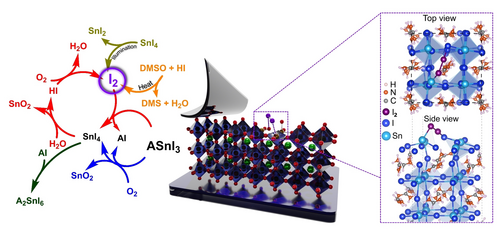
Left: chemical pathways leading to I2 formation in Sn HaPs, i.e. photoreduction of SnI4 (yellow),21 decomposition of DMSO to dimethyl sulfide (DMS, orange),15 O2- and H2O-driven degradation of Sn HaP (blue and red).8 Right: degradative interaction of I2 with the (001) FASnI3 surface simulated via first principles calculations. Reproduced with permission from ref. 8.
2.1 Formation of I2 in Sn HaPs
Saidaminov et al. observed that dimethyl sulfoxide (DMSO), a commonly employed solvent in perovskite precursor solutions, can oxidise SnI2 to SnI4 upon heating.19 A detailed investigation by Pascual et al. identified that native hydroiodic acid (HI) can promote the DMSO-mediated degradation of SnI2 to SnI4, proposing I2 formation in this process as the reason behind the oxidation of Sn2+ in solution.15
Recently, we explored Sn HaP film decomposition under ambient environmental conditions (O2+humidity) and detected SnI4 as a result of an O2-driven degradation process,8 in agreement with previous reports.20 A key feature of SnI4 is its rich chemical reactivity which can impact stability. Indeed, we showed that SnI4 can either i) combine with iodosalts (AI, where A is a monovalent cation) and generate a vacancy-ordered double perovskite analogue (A2SnI6) or ii) more importantly, participate in a hydrolysis reaction with H2O to give HI, which in turn reacts with O2 to form I2. The halogen (I2) was then shown to further decompose perovskite (Figure 1, right) and produce more SnI4 in a cyclic degradation process. In essence, this mechanism causes the breakdown of perovskite triggered by moisture and O2, where native iodide ions in the lattice evolve to form aggressive I2 species.
Further pathways leading to I2 formation have also been identified by Sanchez-Diaz et al. Specifically, they reported the presence of a light-activated ligand-to-metal charge transfer (LMCT) process in SnI4 within the perovskite leading to the formation of I2 and SnI2.21
Altogether, the formation of I2 can occur through multiple chemical reactions and conditions (e.g. solution and solid-state; inert atmosphere and ambient conditions; dark and under illumination).
2.2 Halide Substitution in Sn HaPs
Despite its key role in determining materials stability, the number of studies addressing the presence and effect of I2 as an oxidiser within Sn HaPs remains limited. As per Pb HaPs, it is likely that reducing the number of intrinsic point defects and improving the morphology of the film will improve the tolerance to ambient conditions and halogen formation.22 Another approach may be the in situ neutralisation of I2 through the addition of sacrificial reductants to Sn HaPs, such as NaBH4.21 While these strategies are helpful to improve material and device stability, only limiting the intrinsic ability of Sn HaP to form I2 is expected to address the root cause of halogen-mediated degradation.
The substitution of X-site I− in the ASnX3 perovskite structure with bromide (Br−) is one approach to mitigate I2 formation in Sn PSCs. Based on the trend of halogen oxidation strength (F2>Cl2>Br2>I2), the removal of I− by Br− will most likely result in a weaker tendency of Sn HaP to form halogens. Similarly, Sn4+ compounds containing Br− are less susceptible to undergo LMCT photoreduction reported for SnI4, thus limiting halogen evolution.23 In terms of lattice energy, the smaller ionic radii of Br− lead to stronger Sn−X bonds relative to I−, further increasing the stability of the perovskite system. Due to their small size, the remaining halides (Cl− and F−) do not easily incorporate into lattice X sites;24 however, the use of SnF2 or SnCl2 VSn filling additives to sequester Sn4+ in solution may be beneficial by limiting the presence of the species that can trigger halogen formation as per the mechanisms reviewed above (i.e. SnI4, HI; see Figure 1, left).
Sn HaPs prepared with high fractions of Br− have been shown to exhibit high stability, with i) Ippili et al. demonstrating that MASnBr3 (where MA is methylammonium) can retain its crystal structure with minimal changes over 4 months in ambient conditions (Figure 2a)25 and ii) Lee et al. and Zhu et al. reporting higher optical stability after 100 h (Figure 2b) and lower free carrier densities in Br-substituted FASnI3 (where FA is formamidinium) and MASnI3, respectively.26, 27 This suggests that the evolution of Br2 does not readily occur in the same way as I2. In addition to the thermodynamically unfavourable oxidation of Br− and the increased Sn−Br bond strength, the lack of Br2 most likely originates from a stronger hydrogen bonding between the A-site ammonium/amidinium hydrogens and Br− ions relative to I−.28 Furthermore, I− replacement with smaller Br− reduces the unit-cell dimensions, producing a more compact lattice that can potentially block O2 and moisture ingress; these being key factors in the conversion of SnI4 to I2.
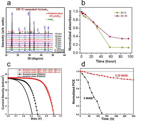
a) X-ray diffraction patterns of MASnBr3 showing no changes in structure after 4 months of ambient aging. Reproduced with permission from ref. 25. b) Optical degradation test of FASnI3−xBrx showing higher ambient stability in mixed-halide compositions (x=0.25). Reproduced with permission from ref. 26. c) Current density–voltage curves of Sn HaP solar cells with varying Br− content and d) their operational stability tests under AM1.5 light soaking. Reproduced with permission from ref. 31.
The benefits of incorporating small fractions of Br−/Cl− can also be extended to the performance of fully functioning optoelectronic devices. It is noteworthy that the only two literature examples reporting Sn HaP solar cell efficiencies exceeding 14 % include small fractions of Br− in the absorber layer.29, 30 The inclusion of Br− has been shown to deactivate non-radiative carrier recombination and improve the film microstructure. However, only a few reports have assessed the role of halide substitution in the chemical and operational stability of Sn HaP materials and devices. Lee et al. demonstrated that substituting 25 % of I− by Br− in FASnI3 not only improves device performance but also leads to i) a decrease of three orders of magnitude in free hole concentration and ii) better stability of encapsulated solar cells (84 % of initial efficiency kept after 1000 h under AM1.5 G light exposure).26 Similarly, Yu et al. reported solar cells based on MA0.25FA0.75SnI2.75Br0.25 with efficiencies of 9.31 % in contrast to 5.02 % in FASnI3 devices (Figure 2c). Devices with 25 % Br− retained 80 % of their performance after 300 h, outliving I−-based devices (Figure 2d).31 These improvements in stability have been attributed to an increase in VSn formation energy and higher crystal orientation upon Br− incorporation. However, we hypothesise that limiting the I− content in Sn HaPs may also mitigate halogen formation and p-type doping pathways [Figure 1 (left) and Eq. (4) and (5), respectively]. In line with this, Khan et al. proposed that the addition of Br− to Sn HaPs increases the formation energy of iodide vacancies (VI), limiting harmful HI generation and accounting for the lower Sn4+ content in Br−-substituted films.32
The addition of Br− leads to a trade-off between light harvesting capability and intrinsic materials stability.33 Therefore, the need to retain an ideal band gap (for solar cell devices) limits the fraction of native I− that can be replaced by Br−. However, opportunities for high Br− fraction, wide band gap perovskites may emerge in tandem solar cells,34 transistors27 and visible light emitters (see Section 4).35, 36
3 Ecological Impact
Monitoring metal uptake by plants provides a simple way to assess the biological impact of HaPs. Li et al. evaluated Pb and Sn capture by growing mint on soil contaminated with MAPbI3/MASnI3 precursors.37 Upon adding 5 mg kg−1 of Pb/Sn HaP to soil, mint roots show a Pb uptake coefficient (defined as the metal content increase in plants relative to contaminant concentration added to soil) of ≈300 % (effects in plants shown in Figure 3a), while for Sn this is ≈40 %. These results highlight the lower bioavailability of Sn compared to Pb, suggesting that Sn HaPs may offer a safer technology with lower bioaccumulation.
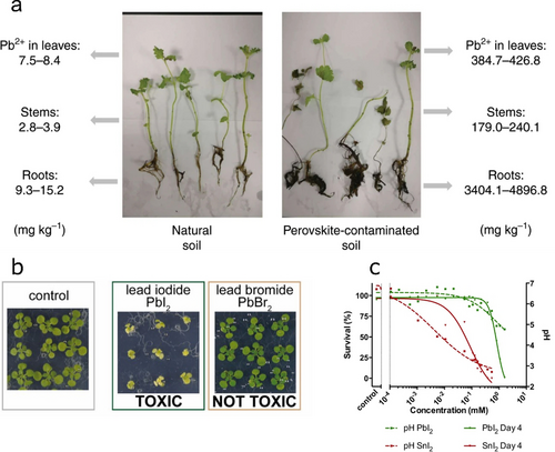
a) Pb uptake values of mint plants grown in natural soil (left) and in perovskite-contaminated soil (right, 250 mg kg−1 MAPbI3). Reproduced with permission from ref. 37. b) Toxicity effect of I− vs Br− ions from perovskite precursors in Arabidopsis plants. Reproduced with permission from ref. 38. c) Correlation between zebrafish embryo survival and pH in PbI2/SnI2-contaminated aqueous medium. Reproduced with permission from ref. 40.
To assess the toxicity of HaPs holistically, it is important to consider the effect of all constituting ions as well as the interplay between them. In the previous study by Li et al., the presence of MA+ was shown to exacerbate metal uptake, presumably by causing changes in soil pH.37 The contribution of halides in HaPs to plant toxicity was recently investigated by Hutter et al;38 MAPbI3 and its precursors were shown to induce smaller plants and lower chlorophyll production (Figure 3b) at much lower concentrations than Br−-based precursors MABr and PbBr2 (5 vs 500 μM). While I− itself is considered a micronutrient in plants,39 its chemical nature when in HaPs possibly accentuates the negative effects caused by the metal and the organic components. Further studies looking into the ecological impact of I−-poorer compositions are pertinent to develop more eco-friendly HaPs.
 (6)
(6) (7)
(7)Hydrohalic acids [HI in Eq. (6) and (7)] thus represent the main safety challenge in Sn HaPs. To limit the ability of Sn HaPs and their degradation products to hydrolyse, it is therefore critical to increase their stability in water; water-resistant coatings such as Al2O341 and the synthesis of perovskites terminated with insoluble layers42 offer promising opportunities. Alternatively, the incorporation of metal-sequestrating materials in devices such as chelating agents43 and cation-exchange resins/minerals44, 45 is a reasonable approach to limit the interaction of Sn halides with water.
4 Visible Sn HaP Emitters
Archetypal I−-based Sn HaPs (e.g. MASnI3) exhibit near ideal band gaps for solar cells (≈1.30 eV). However, this limits their emission to the near-infrared region.36, 46 Substitution of I− with Br− provides an attractive approach to tune the emission properties of the perovskite. For example, Lai et al. showed that the partial incorporation of Br− in MASnI3 gives LEDs emitting up to ≈667 nm (50 % Br−).36 Bandgap broadening upon halide substitution can be rationalised by i) stronger electron confinement in shorter metal−halide bonds leading to shallower conduction band minimum and ii) higher electronegativity in smaller halides causing deeper valence band maximum.47
4.1 Two-Dimensional Sn HaP Emitters
Two-dimensional (2D) Sn perovskites offer superior emission properties in the visible region (from ≈450 nm to ≈650 nm) as compared to their 3D counterparts.35 Layered perovskites incorporate bulky organic cations in the A-site (Figure 4a), leading to higher stability and wider band gaps.48 Bandgap broadening arises from stronger carrier confinement,49 which in turn leads to exciton binding energies of over an order of magnitude higher in 2D perovskites relative to their 3D analogues.50 In our previous work, we demonstrated that transitioning from MASnI3 to (PEA)2SnI4 (PEA=phenylethylammonium) causes a blue-shift in the emission from ≈950 nm to ≈630 nm.35 Furthermore, we found that 2D perovskites possess superior optoelectronic properties (i.e. longer charge carrier lifetime, higher photoluminescence quantum yield or PLQY). Hence, we reported the first use of such materials (e.g. (PEA)2SnI4) in visible light LEDs. Since our initial work, research efforts within the scientific community have focused on improving the performance of red 2D Sn HaP LEDs. To this end, a number of strategies have been explored including: i) crystal growth engineering to yield more uniform thin films,51-53 ii) dielectric confinement enhancement through organic cation replacement54, 55 and iii) the use of antioxidant additives.56, 57 To date, (PEA)2SnI4 remains the champion 2D Sn HaP emitter, with record external quantum efficiencies (EQE) in LEDs of 5 % (Figure 4b)57 and showing promising upscaling prospects.58
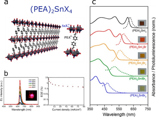
To attain efficient visible emission beyond red, quantum size effects in 2D HaPs must be combined with I− substitution by smaller halides (e.g. Br−), as shown for three-dimensional (3D) structures. Exploiting this approach, we showed that the emission of (PEA)2SnI4 can be tuned from ≈630 nm to ≈470 nm by progressively replacing I− by Br− (Figure 4c).35 This wide emission range makes 2D Sn HaPs interesting candidates for next-generation LEDs with low toxicity. However, PLQY losses and lower photoluminescence (PL) lifetimes persist as unwanted consequences of Br- incorporation,35, 59 which make the design of efficient blue Sn HaP LEDs challenging.
4.2 Broadband Sn HaP Phosphors
The use of larger surface-to-volume ratio systems offers a route to more emissive Br−-based Sn HaPs. For example, Shellaiah et al. demonstrated a PLQY of over 14 % in ligand-stabilised MASnBr3 quantum dots.60 It is possible that ligand-mediated surface passivation may mitigate Br−-related losses by reducing energetic disorder. An additional route to boost light emission in Br−-based materials involves the use of strongly confined emitters based on long alkyl chain spacers or even zero-dimensional hybrid structures (Figure 5a). This has led to extremely long-lived emission with PLQYs that often approach unity. For example, Zhou et al. achieved PLQYs around 95 % for 0D (C4N2H14Br)4SnBr6,61 whereas Zhang et al. reported PLQYs up to 88 % for 2D (C18H35NH3)2SnBr4.62 Efficient radiative recombination arises from stronger electron–phonon coupling in the fully isolated inorganic regions, favouring exciton self-trapping and yielding broadband phosphorescence (Figure 5b,c). Interestingly, this class of Sn HaPs exhibit outstanding stability under a great variety of stressors (i.e. illumination, heat and ambient conditions).63 The substitution of I− by Br− remains an effective route to increase the stability of low-dimensional Sn HaP emitters; Zhou et al. demonstrated that (C4N2H14Br)4SnBr3I3 shows higher photostability under illumination vs (C4N2H14I)4SnI6,64 following the same rationale as in their 3D counterparts (see above). Overall, these features make Sn HaP phosphors strong candidates for lighting applications beyond monochromatic light such as white-light phosphorescent devices.
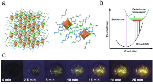
a) Structure of (C4N2H14Br)4SnBr6 zero-dimensional phosphor (left) and close-up view of SnBr64− octahedra isolated by C4N2H14Br+ ligands (right); b) process of exciton reorganisation (self-trapping) and broadband emission. Reproduced with permission from ref. 61. c) White-light phosphorescent effect of one-dimensional C4H14SnBr6 under UV irradiance. Reproduced with permission from ref. 63.
5 Outlook: Lessons from Pb HaPs
Unlocking the full potential of Sn HaPs optoelectronics inevitably requires the application of strategies proven useful in their Pb counterparts. This section describes how two popular avenues in Pb HaP solar cells, i.e. defect management and interfacial engineering, can be applied to address issues in Sn HaP devices arising from their halide chemistry.
5.1 Halide Defect Management
In the most studied Pb-based perovskite material, i.e. MAPbI3, it is well established that its constituent ions, and especially I−, migrate upon external stimuli (e.g. bias or illumination).65, 66 Eames et al. identified that VI play a key role in this process by enabling hopping of I− (Figure 6a),65 while Minns et al. demonstrated that I− can further move through Ii positions via the rearrangement of MA+ and even form neutral I2 within the perovskite lattice.67 These processes are known to profoundly affect the electronic properties of Pb HaPs by generating trap states and promoting halogen formation. It is reasonable to suppose that such processes can also occur in Sn HaPs. To overcome this, treatments targeting I−-related defects are useful to increase both performance and stability of Pb HaPs; we envisage these strategies to benefit Sn HaPs in a similar manner. Yang et al. introduced additional I− into the organic cation solution to decrease the amount of deep level defects.68 This route yielded power conversion efficiencies of over 22 % and 19 % for small and large area devices, respectively. Our own approach consisted of applying post-treatment solutions comprising I− salts onto MAPbI3 films to fill VI.69 In our previous work, we demonstrated that upon light and O2 exposure VI act as preferred sites for the formation of superoxide (O2−) species harmful to perovskite (Figure 6b).69-72 Deactivating O2− formation pathways via VI filling also translates into enhanced operational stability in solar cells.69 While O2− formation in Sn HaPs is unlikely due to their prompt reaction with O2, passivating halide defects remains important in order to limit potential halogen evolution pathways derived from ion migration.
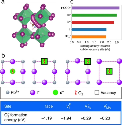
a) I− migration via VI simulated with density functional theory. Reproduced with permission from ref. 65. b) Possible O2− formation sites in MAPbI3 and their corresponding formation energies, identifying VI as the most favourable. Reproduced with permission from ref. 69. c) Calculated binding affinity of pseudohalides to FAPbI3 surface. Reproduced with permission from ref. 74.
Caution must be exercised upon treating HaPs with I−-based salts; Tan et al. showed that Ii defects may arise from such post-treatments, promoting unwanted cubic-to-hexagonal phase transitions in FAPbI3 absorbers73 and potentially making more I− available for halogen formation in Sn HaPs. As a universal strategy, Jeong et al. recently reported the use of pseudohalide additives for defect elimination in HaP materials.74 While Br− and Cl− show superior binding affinity to VI vs I−, formate (HCOO−) pseudohalide provides the strongest interaction in FAPbI3 (Figure 6c), leading to i) certified photovoltaic efficiencies of 25.2 %, ii) high operational stability (≈450 h) and iii) bright electroluminescence with EQE over 10 %. While pseudohalides have been implemented in Sn HaPs to control film growth,75 further additive engineering efforts will continue to enable effective halide defect management strategies.76 Other methods to mitigate crystallographic defects such as aerosol-assisted solvent treatments are readily applicable in Pb-free perovskite technologies.77
5.2 Interfacial Engineering
A wide range of interface engineering strategies have been developed and successfully utilised to improve both the performance and stability of Pb HaP solar cells. For example, regulating Lewis acid–base interactions at HaP/charge transport layer junctions by selecting suitable passivating moieties in the latter is integral to allow efficient charge transfer.78 However, such approaches remain virtually unexploited in Sn HaPs. We recently observed the ambient stability of (PEA)0.2(FA)0.8SnI3 deposited onto hole transport layers (HTLs) to correlate with the hole extraction ability of the substrate (Figure 7a,b).8 Here we proposed that the fast removal of holes in perovskite may help to mitigate Sn2+-to-Sn4+ oxidation and the evolution of labile SnI4 and enhance stability; this being consistent with the molecular oxygen and moisture-driven degradation mechanism in Figure 1. Moreover, enhancing anodic contact selectivity in Sn HaP optoelectronics therefore serves as a key device design rule for the realisation of efficient and stable solar cells. A particularly interesting approach involves novel nanomaterials that can extract charges from the device more effectively. Recently, we employed a newly discovered nanomaterial (i.e. phosphorene nanoribbons, PNRs) to improve hole extraction in Pb HaP solar cells (Figure 7c).79 MAPbI3-based solar cells utilising a PNR/poly(triaryl)amine (PTAA) HTL were shown to exhibit power conversion efficiencies over 21 %, a figure comparable to those in single-crystalline MAPbI3 solar cells.80 We also exploited ferrocene as a perovskite surface potential modifier at (FAPbI3)0.95(MAPbBr3)0.05/spiro-OMeTAD (HTL) junctions.81 This avenue yielded i) enhanced charge transfer from perovskite to spiro-OMeTAD (Figure 7d,e) and ii) highly efficient solar cells (23.45 %) with high operational stability (70 % performance retention after 1250 h). Similarly, we demonstrated that ultrathin polymethylmethacrylate (PMMA) interlayers can effectively enhance selectivity at PEDOT:PSS/(PEA)0.2(FA)0.8SnI3 interfaces and boost solar cell performance from 6.5 % to 10 % (Figure 7f).82 While PMMA interlayers are expected to be beneficial to the operational stability of Sn HaP solar cells, further research in this direction is needed. We expect these approaches to boost hole extraction in archetypal Sn HaP device architectures based on PEDOT:PSS and other less commonly employed HTLs such as nickel oxide (NiOx)83 or ambipolar tin oxide (SnOx).84 Recently, Song et al. demonstrated the use of self-assembled monolayers (SAMs) on indium tin oxide (ITO) anodes in p-i-n, FASnI3-based solar cells.85 As also shown in Pb and mixed Sn–Pb HaP devices,86, 87 we expect chemically tailored SAMs to become next-generation hole-selective contacts in Sn HaP optoelectronics.
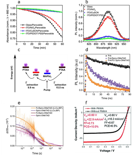
a) Optical degradation test of HTL/(PEA)0.2(FA)0.8SnI3 samples under ambient conditions and b) their quenched PL spectra consistent with hole extraction to HTL. Reproduced with permission from ref. 8. c) PNRs yield faster hole extraction in PTAA/MAPbI3 junctions. Reproduced with permission from ref. 79. d) Time-resolved PL decays and e) transient absorption spectroscopy kinetic traces showing enhanced photoinduced charge transfer (i.e. higher hole injection yield) at perovskite/HTL junctions upon ferrocene treatment. Reproduced with permission from ref. 81. f) Current density–voltage curves of (PEA)0.2(FA)0.8SnI3 solar cells with/without PMMA interlayer engineering. Reproduced with permission from ref. 82.
Though not being the main focus of this Minireview, the importance of interfacial chemistry at Sn HaP/electron transport layer (ETL) junctions should not be disregarded. Considering that I2/I3− can be found at the surface of Sn HaPs even in freshly made samples,21 the design of Sn HaP/ETL interfaces tolerant to such degradation products (Figure 1) also warrants future research efforts. For this, the design and application of interlayers that can react with native I2 in Sn HaPs is a promising direction. Exploiting the tendency of I2 to bind to polymeric materials88 may serve as an opportunity to scavenge the halogen out of Sn HaPs as it is generated. Kang et al. recently employed a polyvinylpyrrolidone–I2 complex to passivate grain-boundary defects in Pb HaP solar cells;89 we propose that the I2-capturing ability of polyvinylpyrrolidone can similarly be applied in in situ protective layers for Sn HaPs.
6 Conclusions
This Minireview highlights the importance and implications of halide chemistry on the stability, ecological impact and optoelectronic device performance of Sn HaPs. It is now becoming widely accepted that the evolution of native I2 in perovskites can trigger the degradation of Sn HaPs. A simple approach to mitigate this process involves the partial substitution of I− by less reactive Br−; we envisage this avenue to become widespread for future breakthroughs in solar cells. Although Sn HaPs offer low bioaccumulation, water/soil acidification via hydrolysis of Sn halides remains a major environmental concern. As such, the development of methods to hinder such hydrolysis is urgently required. In this context, two attractive pathways involve the development of i) Sn HaPs with innate resistance to water and/or ii) Sn-sequestrating agents. Efficient and stable visible-emitting Sn HaPs lighting technologies can be realised through the combination of halide engineering and low-dimensional perovskite structures. In particular, strongly-confined, Br−-based Sn HaPs show great potential as white-light phosphorescent emitters. Finally, identifying ion motion phenomena in Sn HaPs and implementing lessons from Pb HaP solar cells on halide defect neutralisation (e.g. VI filling) and device interface engineering (e.g. contact selectivity enhancement) may enable strategies to tackle I2-induced degradation and boost efficiency. Unravelling the intricacies of halide chemistry in this class of materials will open up a myriad of possibilities in Sn HaP optoelectronics.
Acknowledgments
S.A.H acknowledges financial support from the Engineering and Physical Sciences Research Council (EPSRC grant number EP/R020574/1). T.J.M thanks the Royal Commission for the Exhibition of 1851 for their financial support through a Research Fellowship.
Conflict of interest
The authors declare no conflict of interest.
Biographical Information
Luis Lanzetta is a Postdoctoral Fellow in the KAUST Solar Center at King Abdullah University of Science and Technology. He obtained his PhD in Chemistry at Imperial College London in the group of Prof Saif A. Haque, working on the synthesis and characterisation of lead-free perovskites for use in photovoltaic and light-emitting applications. His research focuses on molecular doping approaches for halide perovskite semiconductors and the study of degradative processes in nanostructured hybrid materials for the design of stable energy conversion applications.
Biographical Information
Thomas Webb is a postgraduate researcher in the department of Chemistry at Imperial College London. He holds masters degrees in both Chemistry and Electronics and Electrical Engineering from Imperial College London and the University of Surrey, respectively. He is currently conducting his doctoral studies at Imperial College London investigating the use of novel reductants and developing new strategies to stabilise tin perovskites under the supervision of Prof Saif A. Haque.
Biographical Information
Jose Manuel Marin-Beloqui is a Maria Zambrano Fellow at the University of Málaga (Spain). His research focuses on the use of transient absorption and Raman spectroscopies to elucidate the excited state dynamics of different materials for use in organic electronics. Previously, he was a postdoctoral researcher at University College London and Imperial College London, analysing charge transfer processes in a wide range of third-generation photovoltaic devices.
Biographical Information
Thomas J. Macdonald is an 1851 Research Fellow in the School of Engineering and Materials Science at Queen Mary University of London. He also holds an Honorary Visiting Researcher position in the Department of Chemistry at Imperial College London. Prior to this, he was a Fellow at Imperial studying the charge carrier dynamics of novel nanomaterials in optoelectronics. From 2017–2019, he was a Ramsay Memorial Fellow at University College London developing new nanomaterials for solar energy conversion. He has a strong interest in renewable energy and extensive experience in the synthesis of functional nanomaterials and the fabrication of third-generation photovoltaics.
Biographical Information
Saif A. Haque is a Professor of Chemistry at Imperial College London. He is a physical chemist with a particular interest in nanomaterials, electronic materials, photochemistry and solar energy conversion. His research is currently addressing the functional characterisation and development of solar cell absorbers and devices based upon solution processable hybrid inorganic–organic semiconducting materials, inorganic metal chalcogenides, quantum dots and perovskites. Prior to becoming a professor, he was a Royal Society University Research Fellow at Imperial between 2005 and 2013.


