Repairing Nanoparticle Surface Defects
Graphical Abstract
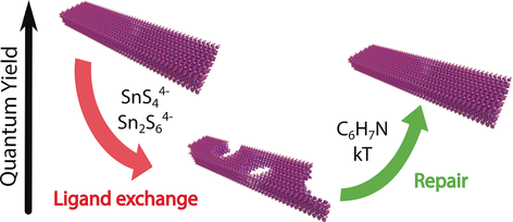
Solar devices based on semiconductor nanoparticles require the use of conductive ligands; however, the exchange of insulating ligands with conductive metal chalcogenide complexes introduces structural defects that act as traps for charge carriers. CdSe nanoplatelets were used as a model system to show that it is possible to minimize the formation of defects, as well as trigger surface healing, by a judicious choice of mild treatments.
Abstract
Solar devices based on semiconductor nanoparticles require the use of conductive ligands; however, replacing the native, insulating ligands with conductive metal chalcogenide complexes introduces structural defects within the crystalline nanostructure that act as traps for charge carriers. We utilized atomically thin semiconductor nanoplatelets as a convenient platform for studying, both microscopically and spectroscopically, the development of defects during ligand exchange with the conductive ligands Na4SnS4 and (NH4)4Sn2S6. These defects can be repaired via mild chemical or thermal routes, through the addition of L-type ligands or wet annealing, respectively. This results in a higher-quality, conductive, colloidally stable nanomaterial that may be used as the active film in optoelectronic devices.
Colloidal semiconductor nanocrystals (NCs) represent a versatile class of materials with unique optoelectronic properties that are fundamentally defined by their nanometric confinement. The use of NCs in optoelectronic devices ranges from optical displays1 and transistors2 to solar cells.3 Specifically, photovoltaic devices fabricated from NCs are amenable to inexpensive room-temperature solution processing, with the promise of yielding large-scale thin films.4 Power conversion by a solar cell requires, in sequence, light absorption, charge carrier separation, charge transport to, and extraction at the contacts. Whereas light absorption can be optimized by the choice of material, for example, by tuning the NC composition, size, and shape, charge carrier separation and transport within the macroscopic film are limited by the NC surface properties, requiring the presence of conductive pathways between individual nanocrystals. Metal chalcogenide complexes have been used as conductive surface ligands that improved charge transport in devices;5 however, replacing the native insulating ligands requires an often detrimental ligand exchange (LE) process, which greatly reduces the photoluminescence quantum yield (PLQY) by orders of magnitude and decreases the long-term colloidal stability from years to days.5 Insight into the LE process through investigation of a model system would thus be greatly beneficial.
Atomically thin semiconductor nanoplatelets (NPs)6 exhibit superior uniformity in their confining dimension, which is reflected by the coincidence of their ensemble and single-particle PL spectra.6a This key feature results in exceedingly sharp excitonic absorption peaks and band-edge emission with no Stokes shift, which was recently exploited for stimulated emission studies.7 Herein, we utilized NPs as a model system for studying the development of structural defects during LE. Defects in NPs become particularly apparent both topologically and in their PL spectra whereas equivalent changes in quantum dots may be concealed in their intrinsic polydispersity, and thus NPs offer a unique opportunity for investigating LE-induced damage. Surprisingly, we found that defects caused by LE are healed through mild treatments, which led to recovery of the native structural integrity and most of the initial PLQY of the NPs.
We synthesized CdSe NPs with monodisperse lateral dimensions of 94±9 nm×15.5±1.5 nm; the sharp absorption transition at 514 nm is indicative of a thickness of 4.5 atomic monolayers, corresponding to 1.2 nm (Figure 1 a, b; see also the Supporting Information, S1).8 The top and bottom facets, (001) facets of zinc blende CdSe,7b are Cd-terminated and passivated by oleate ligands (OA, one-electron donor or X-type).9 These ligands provide the NPs with colloidal stability in non-polar solvents by steric stabilization but induce stacking of the NPs upon drying (Figures 1 a, S1, and S8). Replacing the insulating oleate ligands with conductive metal chalcogenide complexes is a necessary step to achieve sufficient electronic transport in thin films.5a, 10 To this end, we used a two-phase system in which a solution of thiostannate ligands (Na4SnS4 or (NH4)4Sn2S6) in a polar solvent, such as an aqueous solution of NH4OH, was placed in contact with a dispersion of NPs in hexane (see the Supporting Information for details). Stirring the mixture allowed for LE to proceed until the NPs had fully migrated to the polar phase. After ligand exchange, the NPs were still well dispersed as shown by dynamic light scattering (DLS) measurements, which revealed only minor changes in the hydrodynamic radius between pristine and LE NPs (Figure S8). Remarkably, DC conductivity studies showed that the conductance of a non-annealed thin film of LE NPs is up to three orders of magnitude higher than that of pristine NPs, yielding an electron mobility value of approximately 0.5×10⁻³ cm2 V−1 s−1 (Figures 1 c and S10). To the best of our knowledge, this is the first report of conductivity for NPs passivated with thiostannate complexes. Concomitant with the strong increase in conductance, however, a dramatic degradation of structural integrity was observed for the ligand-exchanged NPs, seen as punctures in the atomic crystal lattice (Figures 1 d and S2–S4); at the same time, the PLQY greatly decreased (Figure 1 b). The direct observation of the development and propagation of surface defects is enabled by the exceptionally thin NPs as the removal of just a few atoms from the (001) facets strains the lattice, inducing perforations. 8a While the aqueous solution of NH4OH, itself an L-type (two-electron donor) promoter ligand, enables the LE with thiostannate ligands to proceed rapidly, 9a it also supports degradation, likely following a process known as L-promoted Z-type ligand displacement. Calibrated HAADF STEM images showed that at least 50 % of the material was removed from the damaged areas (Figure S4 d, e). These results highlight the mobility of surface atoms in such II–VI NCs.
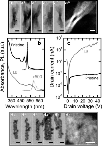
CdSe NPs before and after ligand exchange (LE) with Na4SnS4. a1–a5) Bright-field STEM and a6) high-resolution HAADF images of pristine NPs with OA as the ligand. b) Absorbance (solid lines) and PL (dotted lines) spectra of pristine and LE NPs. The PL intensity of the ligand-exchanged NPs has been multiplied by 500. c) DC conductivity measurements on thin films of pristine and LE NPs. d1–d5) Bright-field STEM and d6) high-resolution HAADF images of damaged NPs with (NH4)4Sn2S6 as the ligand. Black scale bars: 20 nm; white scale bars: 5 nm.
We found this structural and PLQY degradation to be quite general. The displacement potency of a ligand depends on multiple attributes, such as electronic effects, chelation, and steric properties. 9a We varied the latter by replacing NH4OH with another promoter ligand pyridine, 3-methylpyridine, or 2,6-dimethylpyridine (DMP), which are all L-type ligands, and found that all LE treatments resulted in perforation of the NPs; furthermore, treatment with DMP also resulted in material rearrangement from the NP core onto the surface (Figure S2). This structural damage always correlated with a dramatic decrease in PLQY (ca. 0.02 %) with respect to the original pristine NPs with oleate ligands (10 %). We also studied LE-induced damage in the absence of promoter ligands that may trigger L-promoted Z-type ligand displacement, by altering the composition of the polar phase from pure water (ϵ≈80) to N-methylformamide (NMF, ϵ≈182). Interestingly, while the use of water still resulted in heavily damaged NPs, NMF did not induce visible perforations (Figure S2 e, f). This finding supports a recent study that described the removal of only oleate ligands upon LE with thiostannate complexes when using NMF, therefore leaving the Cd-rich surface intact. 10b Nevertheless, the PLQY dramatically decreased to approximately 0.01 %. Thus while a judicious choice of the polar component during LE can reduce structural damage, the effects on the spectroscopic properties remain deleterious. We therefore studied the healing of NPs after LE in the presence of NH4OH. Unexpectedly, upon addition of DMP to an already damaged dispersion of NPs with Na4SnS4 as the ligand, we observed the recovery of the structural integrity and the healing of holes, with no measurable changes in the NP lateral dimensions (Figures 2 a, S4, S5, and S7). Additionally, the PLQY underwent a tenfold increase, indicative of the recovery of crystalline integrity of the NPs together with an improved surface passivation, and the absorption spectrum was slightly blue-shifted as a result of the effective decrease in the local NP thickness through the removal of rough areas (Figure 2 b).
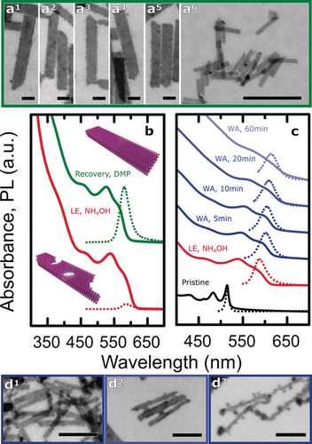
Healing defects in the NP crystal lattice with DMP. a1–a6) Bright-field STEM images of repaired NPs after DMP treatment with Na4SnS4 as the ligand. Scale bars: 20 nm (a1–a5) and 200 nm (a6). b) Absorbance (solid lines, normalized) and PL (dotted lines) spectra of NPs after LE and after DMP treatment. c) Wet annealing (WA) of NPs at 100 °C. Absorbance (solid lines, normalized) and PL (dotted lines, normalized) spectra for pristine NPs, after LE with Na4SnS4, and during WA. d) Bright-field STEM images of NPs after 5 min (d1), 20 min (d2), and 60 min (d3) of WA. Scale bars: 50 nm.
As an alternative to chemical treatments, we also explored temperature treatments without DMP as the healing process should depend on the thermal energy supplied. We investigated this by performing a wet annealing (WA) treatment, starting from a dispersion of damaged NPs in water and increasing the temperature of the solution to 100 °C. Immediately thereafter, the dispersion slightly changed in color; we continued to follow the structural and spectroscopic changes by taking aliquots every few minutes (Figure 2 c). After 5 min of WA, the absorption and PL peaks underwent a red shift of about 10 nm, suggesting structural modification of the NPs; remarkably, the PLQY recovered by a factor of 230 compared to the values measured after LE, reaching 4.5 %. As the WA proceeded, the absorption and PL peaks were red-shifted by an additional ca. 5 nm after 10 min; the excitonic peaks of the absorption lost definition, the scattering was enhanced, and the PL spectrum broadened. Direct visualization of the NPs after WA by STEM revealed surface reconstruction, yielding whole NPs (Figure 2 d). Similarly to the DMP treatment, WA leads to NP recovery, confirming the enhancement of the surface mobility under mild conditions. The process eventually triggered growth on side facets, bridging NPs together, as demonstrated by both STEM and DLS (Figures 2 d2, S6, and S8 h). Allowing the WA to continue further resulted in the lateral thinning of the NPs along the [1 −1 0] direction and in material overgrowth (Figure 2 d3). Side facets are more favorable to growth and more resistant towards dissolution than top facets owing to both the formation of one extra Cd−Se bond8a and a smaller nucleation energy barrier, as shown in recent work.11 If used in a controlled way, this process can yield surface healing or soldering of NPs. Further nanoscopic details of the NP healing process are revealed by the PL spectra recorded at different stages of recovery (Figure 3 a–c). Pristine NPs passivated with OA showed a second broad PL band at longer wavelengths accompanying the sharp emission profile at the band edge (Figure 3 a), resulting from the presence of deep traps.12 Even in pristine NPs, the QY of this band is comparable to that of the main emission (ca. 5 %). Further disrupting the structural integrity of NPs should result in an increase in the number of defects, and indeed, after LE in the presence of the L-type ligand NH4OH, the defect band strongly increased relative to the band-edge peak (Figure 3 a, b). Remarkably, the nanoscale surface recovery upon DMP addition resulted in a large decrease in the defect band relatively to the main emission peak (Figure 3 b). WA treatment had an even more drastic effect on the recovery of LE-damaged NPs (Figure 3 c): After only 5 min of treatment, the defect band had strongly decreased with respect to the main peak, concomitant with a recovery of the PL of the primary emission. Interestingly, as the annealing proceeded, the intensity of the defect PL band slowly increased. This evolution of the PL spectra directly relates to the structural recovery observed by STEM (Figure 2 d2, d3). While short annealing was beneficial to surface recovery, longer treatment resulted in the overgrowth of material on the NP surface, generating a soldered network.
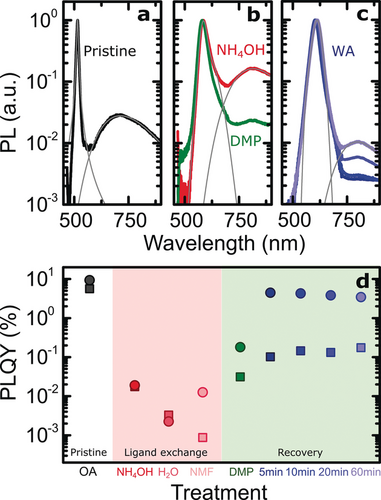
Analysis of the photoluminescence (PL) of nanoplatelets. a) Normalized PL spectra of pristine nanoplatelets with Lorentzian and Gaussian fits (gray lines) for the band-edge and trap state emissions, respectively. Note the log/lin scaling. b) Normalized PL spectra of nanoplatelets after LE and after DMP treatment with Gaussian fits. c) Normalized PL spectra of nanoplatelets during WA. d) Nanoplatelet PLQYs for band-edge (circles) and defect band (squares) emissions for all treatments.
The effect of the recovery processes on the PLQY are summarized in Figure 3 d. Varying the composition of the polar phase during LE affects the PLQY by up to one order of magnitude. Specifically, while for pure water the band-edge PLQY is lower than the defect band contribution, for NMF, it is higher by a factor of 15; these results are supported by, respectively, the presence and lack of perforations in the crystalline structure of the NPs, topological indicators of surface quality (Figure S2). Still, DMP- and WA-healed NPs outperform visually undamaged NMF LE NPs by at least one order of magnitude in terms of the PLQY (Figure 3 d). Additionally, such NMF LE NPs can also be repaired by using the reported DMP and WA recovery routes; also in this case, the PLQY increased significantly, consistent with the NH4OH LE NPs after recovery (Figures S5 and S6).
The effect of structural recovery on the optoelectronic properties was further investigated by time-resolved microwave conductivity (TRMC) measurements, which probe the conductivity within individual NPs. The mean path length of charge carriers measured by this technique is about 30 nm (see the Supporting Information for details); therefore, TRMC measurements uncover the dynamics of photogenerated carriers on the length scale of a single NP. The values for charge carrier mobility in treated NPs correlate well with the PLQY (Figures 4 and S9), confirming that LE introduces traps that can be healed by a mild treatment of the NPs. Importantly, this shows that independent of the extent to which the NP integrity is disrupted during LE, structural repair through chemical and thermal routes can recover a high-quality nanomaterial. Remarkably, the PLQY of the NPs after WA treatment nears 5 %, which is only slightly lower than that of pristine OA-passivated NPs and corresponds to a recovery by a factor of 250 with respect to post-LE NPs. This moderate loss of PL comes at the vital advantage of endowing NPs with conductive ligands that guarantee stability in polar solvents and improved charge transport in optoelectronic devices (Figures S8 and S10).
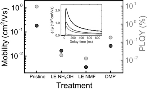
Maximum charge carrier mobility values for treated NPs as measured by TRMC compared to PLQY results for the same samples. The mobility values are given by the maximum of the photoconductance transient shown in the inset when extrapolating for low incident photon flux. Inset: Photoconductance transients for pristine NPs. The incident photon flux increases from the black to the gray curves.
In conclusion, we have demonstrated that CdSe NPs can be used as a convenient model system for studying how LE affects the structural and optical properties of semiconductor nanostructures. While LE with conductive molecular ligands has thus far been mostly limited to quantum dots,10 NPs provide a stringent test case owing to their superior PL line width, large surface area, and convenient flat imaging geometry. As LE on QDs results in a drop in PLQY similar to that observed for our NPs (Figure S11), we believe that these results apply to QDs as well. We have established that LE reactions cause a disruption of the atomic lattice of NCs, thereby introducing defects that quench the PLQY. The composition of the polar phase during the LE proves to be a key parameter in minimizing structural damage, with NMF giving the best results. By understanding the LE-induced structural disruption, we were able to drive the healing of NPs both structurally and spectroscopically by chemical (mild L-type ligands) and thermal (WA) routes. This resulted in a higher-quality and colloidally stable nanomaterial that may be self-assembled into novel structures such as superlattices13 to be used as active films of optoelectronic devices. Future work to microscopically investigate these recovery routes on individual NPs may determine the exact nature of the trapped and recovered states similar to previous works.14
Acknowledgements
We thank D. M. Balazs, Dr. K. Dohnalova, Prof. T. Gregorkiewicz, and Prof. J. Sprakel for helpful discussions. R.W.C. acknowledges support by the Dutch Technology Foundation (now TTW), which is part of The Netherlands Organization for Scientific Research (NWO) under project number 13903. P.S. acknowledges support by a VICI personal grant from the Netherlands Organization for Scientific Research (NWO).
Conflict of interest
The authors declare no conflict of interest.


