Oxygen Vacancies Trigger Rapid Charge Transport Channels at the Engineered Interface of S-Scheme Heterojunction for Boosting Photocatalytic Performance
Abstract
Although oxygen vacancies (Ovs) have been intensively studied in single semiconductor photocatalysts, exploration of intrinsic mechanisms and in-depth understanding of Ovs in S-scheme heterojunction photocatalysts are still limited. Herein, a novel S-scheme photocatalyst made from WO3-Ov/In2S3 with Ovs at the heterointerface is rationally designed. The microscopic environment and local electronic structure of the S-scheme heterointerface are well optimized by Ovs. Femtosecond transient absorption spectroscopy (fs-TAS) reveals that Ovs trigger additional charge movement routes and therefore increase charge separation efficiency. In addition, Ovs have a synergistic effect on the thermodynamic and kinetic parameters of S-scheme photocatalysts. As a result, the optimal photocatalytic performance is significantly improved, surpassing that of single component WO3-Ov and In2S3 (by 35.5 and 3.9 times, respectively), as well as WO3/In2S3 heterojunction. This work provides new insight into regulating the photogenerated carrier dynamics at the heterointerface and also helps design highly efficient S-scheme photocatalysts.
Introduction
Photocatalysis offers a green and sustainable method of converting solar energy to chemical energy with high values, and it has the potential to be an important tool in the fight against climate change and other energy and environmental crises.1-3 The photocatalytic process of semiconductor-based photocatalysts typically consists of the following three stages: 1) photoexcitation-induced charge generation; 2) charge transfer from bulk to the surface of photocatalysts; 3) redox reaction of photogenerated charges with adsorbed molecules on the surface.4 The efficiencies of the three steps jointly determine the overall efficiency of semiconductor photocatalyst. The wide band gap ensures redox capacity of photogenerated carriers, but weakens light-absorption ability, creating an inherent paradox for a single semiconductor photocatalyst.5 Moreover, the photogenerated electrons and holes are prone to recombine, which severely hinders photocatalytic performance.6-8
S-scheme photocatalysts, as the most potential heterojunction structure, shows great advantage in optimizing the charge separation efficiency and enhancing the photocatalytic performance.9, 10 It has been proved that S-scheme photocatalyst can achieve efficient spatial charge separation and high redox potentials of photogenerated carriers simultaneously, which are hard to implement in other types of heterojunctions.11, 12 Generally, a S-scheme heterojunction is composed of an oxidation photocatalyst (OP) with a more positive valence band (VB) and a reduction photocatalyst (RP) with a more negative conduction band (CB). When they come into contact, Fermi level (Ef) difference acts as a driving force, causing electrons to move from RP to OP, resulting in the formation of an internal electric field. After being irradiated, the photogenerated electrons in CB of OP merge with photogenerated holes in VB of RP through this internal electric field. As a result, photogenerated electrons in the CB of RP and the holes in the VB of OP with strong redox abilities are conserved and may participate in photocatalytic reactions.9 It is worth mentioning that the interface regulation of S-scheme is crucial, in which the charge transfer and separation occurs.
Oxygen vacancies (Ovs) as a type of intrinsic defects can adjust the local geometric structure of metal oxides, thus tailoring the physical and chemical properties of metal oxide photocatalysts.13-15 Ovs can alter the band alignment of metal oxides and generate the defect level,16, 17 which play an important role in light absorption.4, 14 Meanwhile, the generation of Ovs in photocatalysts leads to changes in charge separation and transfer process.14 Although the role of Ovs in single component semiconductors has been extensively studied, their modulation mechanism on heterojunction structures, especially in S-scheme heterointerface, lacks in-depth exploration and understanding. Hence, it is highly desirable to unravel the function of Ovs completely at the heterointerface of S-scheme, which may not only bring out the potential of Ovs into S-scheme photocatalysts, but also is beneficial for developing photocatalysts with superior performance.
Herein, a series of novel WO3-Ov/In2S3 S-scheme heterojunction photocatalysts were successfully fabricated, in which Ovs were incorporated into WO3 by the simple hydrogen thermal treatment approach. The lack of oxygen atoms changed the way in which the heterointerface is electronically structured and coordinated. Specifically, the W 5d band was affected by increasing electron densities caused by Ovs anchored with S atoms, forming a close interface connection. This, in turn, acted as a channel for interfacial photogenerated charge transfer. Through femtosecond transient absorption spectroscopy (fs-TAS), it was presumed that the electron trapping states caused by Ovs may trigger additional ways of transporting charges, which led to an increase in charge separation efficiency. In addition, Ovs promoted light absorption, realizing the modulation of thermodynamic parameters of the photocatalytic process. The photocatalytic degradation performance of the optimal sample showed significant enhancement, which was not only 35.5 and 3.9 times higher than that of the single component of WO3 with Ovs and In2S3, respectively. Meanwhile, it was found that the activity of the composite photocatalyst was superior to that of WO3/In2S3 without the introduction of Ovs. These findings will help with the development of new photocatalysts that have even greater efficiency.
Results and Discussion
Design of WO3-Ov/In2S3 Photocatalysts
WO3 nanoparticles with Ovs (WO3-Ov) were prepared by annealing pristine WO3 nanoparticles in 450 °C for 1 h at 5 % H2/Ar atmosphere. In2S3 was subsequently grown on the surface of WO3-Ov via a hydrothermal method. The synthesis process of WO3-Ov/In2S3 heterojunction structure is illustrated in Figure 1a. The obtained samples with different contents of In2S3 are denoted as WOvIn1, WOvIn2, and WOvIn3, while the heterojunction samples of In2S3 grown on pristine WO3 nanoparticles are denoted as WIn1, WIn2, and WIn3. It can be seen from field emission scanning electron microscopy (FESEM) (Figure S1) that the size of pristine WO3 nanoparticles is ~100 nm. After the introduction of Ovs, the morphology remains unchanged. FESEM images show that, as the amount of In2S3 increases, both the surface of WO3-Ov/In2S3 (Figure S2) and WO3/In2S3 samples (Figure S3) are covered with increasing amount of hierarchical structures. Furthermore, transmission electronic microscopy (TEM) confirms the hierarchical architecture of WOvIn2 (inset of Figure 1b). Figure 1b illustrates that the hierarchical In2S3 is composed of plenty of nanoflakes assembled on the surface of the WO3-Ov nanoparticle. It should be noted that this hierarchical morphology can provide a large number of active sites to participate in the photocatalytic reaction, which benefits the photocatalytic performances. In high solution TEM images (HRTEM, Figure 1c), In2S3 displays clear lattice fringes with an interlayer spacing of 0.269 and 0.301 nm, which can be assigned to the (022) and (211) crystal planes of β-In2S3, respectively. Inset of Figure 1c presents the profiles of corresponding lattice fringes. Furthermore, high angle annular dark-field (HAADF) image of WOvIn2 (Figure 1d) and corresponding elemental mapping images of In, S, W, and O (Figure 1e) reveal that hierarchical In2S3 with uniform composition are anchored on WO3-Ov nanoparticles.
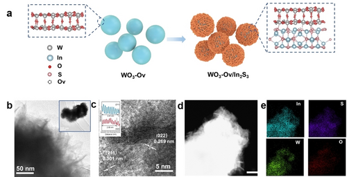
Schematic illustration and micromorphology. a) Schematic illustration of the preparation process of WO3-Ov/In2S3 heterojunction structure. b) TEM images of WOvIn2. c) HRTEM image of WOvIn2. The inset figure is the corresponding line profiles. d) HAADF image of WOvIn2. e) Elemental mapping of In, S, W, and O in the WOvIn2 sample. The scale bar is 100 nm.
Characterization of WO3-Ov/In2S3 Photocatalysts
To detect the unpaired electrons in WO3-Ov, electron paramagnetic resonance (EPR) measurement was carried out. As shown in Figure 2a, the g value at 2.003 corresponds to unpaired electrons in the Ov site.2 It is apparent that after the hydrogen thermal reduction process, the signal area at g=2.003 exhibits significant enhancement, confirming that a considerable number of Ovs were introduced to WO3 with this simple method. X-ray diffraction (XRD) was adopted to figure out the crystal structure of WO3-Ov, In2S3, and WO3-Ov/In2S3. The peaks of WO3-Ov can be well indexed to the monoclinic phase (JCPDS card no. 71–2141), which is consistent with pristine WO3 (Figure S4). It can be concluded that the hydrogen thermal annealing keeps WO3 in its pristine crystal phase. As shown in Figure 2b, the diffraction peaks of In2S3 can be indexed to tetragonal β-In2S3 (JCPDS card no. 84–1385). XRD patterns of WO3-Ov/In2S3 verify the successful synthesis of WO3-Ov/In2S3 heterojunction. Moreover, with increasing content of In2S3 in WO3-Ov/In2S3 heterojunction, the peak intensities of the In2S3 phase increase accordingly. The matching of the XRD peaks of WO3-Ov/In2S3 to those of the combination of WO3-Ov and In2S3 single component indicates that the crystal structure is not altered in the hybridization process. Similarly, XRD patterns of WIn1, WIn2, and WIn3 (Figure S4) also confirm the successful construction of WO3/In2S3 heterojunctions. Raman spectra were conducted to investigate the structural information of the heterojunction. As shown in Figure 2c, Raman peaks of WO3-Ov at 714 and 807 cm−1 can be assigned to the stretching vibrations of longer and shorter W−O−W bonds in WO6 octahedron units, respectively. The peaks at 269 and 331 cm−1 are attributed to the bending vibrations of the bridging oxygen atoms in W−O−W.18 In comparison, the main Raman peak of WO3-Ov demonstrates obvious peak shifting and broadening compared with pristine WO3 (Figure S5a), which is related to the deficiency of oxygen atoms and non-stoichiometry on the WO3 surface.19 The Raman spectra of In2S3 show a distinct peak at 306 cm−1, which is associated with A1g mode of β-In2S3.20 The Raman spectra of WO3-Ov/In2S3 are composed of oscillation peaks of WO3-Ov and In2S3. It can be observed that all the peaks in WO3-Ov/In2S3 shift to lower wavenumber compared with pristine WO3-Ov, confirming the chemical bonding effect between heterointerface.21-23 Raman spectra of WO3/In2S3 are depicted in Figure S5b, where the main peak of WO3/In2S3 shows a similar shift tendency compared with pristine WO3. X-ray photoelectron spectroscopy (XPS) was performed to examine the valence state change of the elements in WO3-Ov/In2S3 heterojunctions. XPS survey spectra (Figure S6) show the existence of W, O, In, and S in this heterojunction. Pristine In2S3 demonstrates two peaks located at 444.8 and 452.3 eV, which correspond to In 3d5/2 and 3d3/2, respectively (Figure S7a). After hybridization, these two peaks shift to higher binding energies. Moreover, W 4 f XPS spectra of WO3-Ov (Figure S7b) demonstrate two peaks at 37.6 and 35.5 eV.18, 24 W 4f peaks of WO3-Ov/In2S3 samples show a negative shift compared with WO3-Ov. After conjunction, S 2p XPS (Figure S8a) shows that S 2p3/2 and 2p1/2 locate at 161.7 and 162.9 eV, respectively.25, 26 Whereas, in these heterojunctions, S 2p3/2 and 2p1/2 shift to higher binding energy. The positive shifts of In 3d and S 2p XPS peaks indicate the loss of electrons in In2S3 upon conjunction.
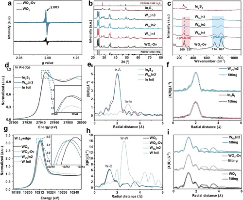
Crystal structures and local chemical environmental characterizations of WO3-Ov/In2S3. a) EPR spectra of WO3 and WO3-Ov. b) XRD patterns and c) Raman spectra of WO3-Ov, In2S3, and WO3-Ov/In2S3 samples. In K-edge d) XANES spectra, e) EXAFS spectra and f) EXAFS fitting spectra of In2S3 and WOvIn2. W L3-edge g) XANES spectra, h) EXAFS spectra and i) EXAFS fitting spectra of WO3, WO3-Ov and WOvIn2.
Meanwhile, O1s XPS (Figure S8b) demonstrates that the lattice O of WO3-Ov/In2S3 moves to lower binding energy compared with WO3-Ov, showing the same peak shifting tendency as W 4 f XPS after hybridization. It can be concluded from W 4 f and O 1s XPS that WO3-Ov accepts electrons after being in contact with In2S3. Further, it can be presumed that upon the contact of WO3-Ov and In2S3 with different Ef, electrons spontaneously transfer from In2S3 to WO3-Ov until Ef is equilibrated at the heterointerface. Consequently, the flow of electrons results in the formation of an internal electric field between the heterointerface of the two semiconductors, pointing from In2S3 to WO3-Ov. XPS of WO3-Ov and WO3 are exhibited in Figure S9 and S10 to compare their chemical states. XPS of WO3/In2S3 are shown in Figure S11, the detailed analysis can be found in Supporting Information.
The electronic structure and coordination environment of In and W before and after conjunction were investigated by X-ray absorption near edge structure (XANES). It can be seen that In K pre-edge peak position of WOvIn2 centers at a higher energy than that of In2S3, indicating that the In element in WOvIn2 possesses higher valence state than that in In2S3 (Figure 2d),27, 28 which is consistent with the In 3d XPS results. Fourier-transformed extended X-ray absorption fine structure (EXAFS) (Figure 2e) was obtained to acquire quantitative structural parameters. It can be noticed that the near-edge absorption energy of WOvIn2 shifts to higher R direction (2.02 Å) with increased intensity compared with In2S3 (1.99 Å), implying that the chemical bonding character of the In2S3 has been changed after the hybridization. Figure 2f presents the fitting result of the extended In K-edge. Table S1 summarizes the quantitative structural parameters fitting result of the extended In K-edge. W L3-edge XANES spectra (Figure 2g) shows that the white line intensity of as prepared WO3-Ov is slightly lower than pristine WO3. The weaker white line absorption peak is related to the increase of W 5d band electron densities in WO3-Ov.29, 30 After the growth of In2S3, WOvIn2 shows a lower intensity peak, revealing the higher average electron density and the decrease of oxidation states of W compared with WO3-Ov, strongly verifying that WO3-Ov accept electrons in this WOvIn2 heterojunction.29 EXAFS spectra of W L3-edge for WO3, WO3-Ov and WOvIn2 are displayed in Figure 2h. EXAFS curve fitting of W-L3 (Figure 2i) shows that compared with WO3, the coordination number in WO3-Ov decreases, which is related to the deficiency of oxygen atoms. Moreover, as for WOvIn2, apart from W−O bond, W−S bond (2.39 Å) as chemical covalent bond forms in WOvIn2. It can be verified that the growth of In2S3 changes the W chemical bonding environment in WO3-Ov samples. The fitting parameters of W L3-edge EXAFS are summarized in Table S2. The wavelet transform contour plots of In K-edge weighted EXAFS for In2S3 and WOvIn2 (Figure S12), and W L3-edge for WO3, WO3-Ov and WOvIn2 (Figure S13) also highlight minor differences in WOvIn2 and the two single components.31 The above results provide evidence that, after the combination, the electrons transfer from In2S3 to WO3-Ov. And the W−S chemical bonding between WO3-Ov and In2S3 is formed at the interface, which may provide an electron transport pathway during photocatalytic process. The microscopic environment and local electronic structure of WIn2 samples are depicted in Supporting Information (Figures S14–S17, Table S3 and S4). The neighboring structure around W atoms and In atoms of WIn2 shows differences compared with WO3 and In2S3 components. k3-weighted EXAFS data and fit data are shown in Figure S18 and Figure S19. Figure S20 shows crystal structure models of In2S3 and WO3 used in EXAFS fitting.
Band Structure Analysis
The light absorption property of the photocatalysts was tested by UV–Vis diffuse reflectance spectroscopy (DRS). As shown in Figure S21, compared with pristine WO3, WO3-Ov shows evidently enhanced photo absorption in the visible region. After hybridization, WO3-Ov/In2S3 heterojunctions show absorption edge from 550 to 580 nm (Figure S22a), which is similar to In2S3. The absorption abilities of WO3-Ov/In2S3 heterojunctions is stronger than that of WO3/In2S3 heterojunctions (Figure S22b), which is beneficial to their photocatalytic properties. The optical photographs of WO3-Ov/In2S3 heterojunctions and WO3/In2S3 heterojunctions are displayed in Figure S23a and S23b, respectively, showing that the existence of Ovs deepens the color of the heterojunctions.
Tauc plot can be obtained based on UV–Vis DRS and Kubelka–Munk equation to analyze the band gap value (Eg) of the semiconductors. As shown in Figure S24, Eg of WO3-Ov and WO3 is estimated to be 2.71 and 2.89 eV, respectively, which verifies that the introduction of Ov can slightly lower Eg. In addition, Eg of In2S3 is calculated to be 2.17 eV. Ultraviolet photoelectron spectroscopy (UPS) was carried out to assess the band structure of the semiconductor photocatalyst. As presented in Figure S25a, the secondary cutoff binding energy ( ) is measured to be 17.01 eV for WO3-Ov. By applying the equation: , the work function ( ) of WO3-Ov can be calculated to be 4.21 eV. Hence, the Ef of WO3-Ov can be determined as −0.19 V (vs. NHE). As shown in Figure S25b, of In2S3 was measured to be 17.36 eV, and Ef of In2S3 can be estimated to be 3.86 eV and −0.54 V (vs. NHE), respectively. Mott–Schottky plots show positive slopes, indicating the n-type behavior of WO3-Ov (Figure S26a) and In2S3 (Figure S26b).32 The conduction band potential (ECB) can be evaluated by Mott–Schottky plots. The flat band potentials (Efb) of WO3-Ov and In2S3 are estimated to be −0.09 and −0.65 V (vs. NHE), respectively.33 It is confirmed by previous studies that ECB of n-type semiconductor is ~0.2 V negative than the Efb.22 Therefore, the ECB of WO3-Ov and In2S3 is estimated to be −0.29 and −0.85 V (vs. NHE), respectively.
Potential of valence band (EVB) can be obtained according to the equation of Eg=ECB - EVB,34 which can be estimated to be 2.42 and 1.32 V (vs. NHE) for WO3-Ov and In2S3, respectively. Figure 3a displays the detailed band structures of WO3-Ov and In2S3 photocatalysts. EPR measurements were performed to further probe the reactive species in photocatalytic reactions, where 5,5-dimethyl-l-pyrroline N-oxide (DMPO) was adopted as a spin-trapping agent. Under light irradiation, hydroxyl ( ⋅ OH) and superoxide ( ⋅ O2−) radicals can be detected. As presented in Figure 3b and 3c, there is no signal observed under dark condition. Once irradiated by light, WO3-Ov is more favorable for generating ⋅ OH− rather than ⋅ O2−, while In2S3 promotes the production of ⋅ O2− instead of ⋅ OH−. These can be attributed to the fact that the VB position of WO3-Ov is more positive than the potential of H2O/ ⋅ OH and CB position of In2S3 is more negative than the potential of O2/ ⋅ O2−.26, 35-37 In WO3-Ov/In2S3 heterojunction structure, the recombination of photogenerated holes and electrons is inhabited effectively, which enables higher amount of photogenerated holes and electrons to oxidize H2O and reduce O2, respectively, causing the enhanced signal of ⋅ O2− and ⋅ OH compared with the individual photocatalysts.38, 39 Moreover, in situ irradiation X-ray photoelectron spectroscopy (ISI-XPS) directly shows the transfer of photogenerated electrons from WO3-Ov to In2S3 under light irradiation (Figure S27a and S27b), the detailed analysis can be found in Supporting Information. The results of EPR and ISI-XPS strongly verify the type of S-scheme heterojunction of WO3-Ov/In2S3. The charge transfer route in this S-scheme heterojunction can be proposed based on the above experiments and calculation results. As shown in Figure 3d, when WO3-Ov and In2S3 contact together, an intimate interface forms. Due to the difference of Ef between the two semiconductors, electrons will spontaneously transfer from In2S3 with higher Ef to WO3-Ov with lower Ef until Ef at the interface reaching equilibrium. Due to the redistribution of electrons on the interface of WO3-Ov and In2S3, the band alignment near the interface changes correspondingly, and an internal electric field is built. In details, WO3-Ov with electrons accumulation shows downward band bending at the interface, while In2S3 with electron loss shows upward band bending. When irradiated by the light, electrons in VB absorb photon energy and jump into CB, causing the photogenerated electrons and holes in CB and VB, respectively. With the joint effect of internal electric field, band bending at the interface and Coulomb interaction, the photogenerated electrons in CB of WO3-Ov tend to transfer to VB of In2S3 and combine with the holes. Through this pathway, the photogenerated carriers with low redox potentials merge, leaving the carriers with higher redox abilities separated apart, which significantly improves the efficiency of photocatalysis. Band structure of WO3/In2S3 is analyzed in details in the Supporting Information (Figure S28 and S29).
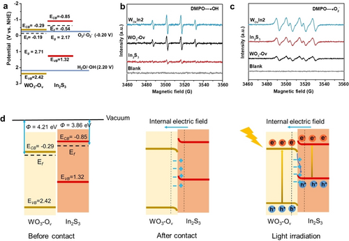
Band alignment and charge transport way at the heterointerface of WO3-Ov/In2S3. a) Band alignment of WO3-Ov/In2S3. EPR spectra of b) DMPO- • OH and c) DMPO- • O2− in the presence of In2S3, WO3-Ov, and WOvIn2, respectively. d) The photocatalytic process of WO3-Ov/In2S3 heterojunction under solar light irradiation.
Photocatalytic and Photoelectrochemical Performance
To evaluate the photocatalytic performance of the heterojunction, Rhodamine B (RhB) degradation property was tested. As shown in Figure 4a, under the irradiation of visible light, WO3-Ov/In2S3 composites show significantly enhanced RhB photocatalytic degradation rate compared with pristine In2S3. Furthermore, the pseudo-first-order equation was utilized to quantitatively evaluate the degradation kinetics of RhB and the fitting curves are illustrated in Figure 4b. It can be seen that WOvIn2 exhibits the highest K values (0.071) toward RhB degradation, followed by WOvIn3 (0.058) and WOvIn1 (0.044). Notably, WOvIn2 shows the optimal performance, which is 8-folds higher than pristine In2S3. The photocatalytic RhB degradation performance of WO3/In2S3 hybridizations is also provided in Figure S30. Pseudo first-order kinetics fitting of RhB degradation of WO3/In2S3 composites is depicted in Figure S31. In order to compare the rate constants (K, min−1) for WO3-Ov/In2S3 and WO3/In2S3, a histogram is depicted in Figure 4c. The photocatalytic RhB degradation abilities of the WO3-Ov/In2S3 heterojunctions are higher than those of WO3/In2S3 composites with the same In2S3 content. It can be presumed that the composites with specific electron transfer channels can remarkably improve the photocatalytic performance. Afterwards, the photocatalytic performance of WOvIn2 was tested for 4 cycles to study its stability. Figure 4d demonstrates that there is no decay during the 4 cycles, revealing the high stability of WOvIn2 S-scheme photocatalyst. The Brunauer–Emmett–Teller (BET) surface areas of all the photocatalysts are summarized in Table S5. K values after normalizing the specific surface are demonstrated in Figure S32 to eliminate the effect of adsorption ability. It can be seen that the creation of Ovs boosts the intrinsic photocatalytic degradation performance and WOvIn2 shows the optimal performance. Furthermore, the photocatalytic phenol degradation performance of the as prepared samples was investigated (Figure S33), the detailed discussions are illustrated in Supporting Information. Transient photocurrent response and electrochemical impedance spectroscopy (EIS) were carried out to study charge transfer and separation efficiency of the photocatalysts. Charge transfer resistance can be evaluated by the semicircle diameter of EIS (Figure 4e). WOvIn2 shows the lowest interfacial charge transfer resistance, verifying the efficient separation of photogenerated carriers. As shown in Figure 4f, the photocurrent density of WO3-Ov/In2S3 hybridizations is higher than that of In2S3 under light irradiation, indicating a higher light harvesting ability and lower carrier recombination rate. Transient photocurrent response of WO3/In2S3 (Figure S34) shows that WIn2 possesses the highest photo response current among WO3/In2S3 composites. Photoluminescence (PL) spectra were collected to investigate the charge transfer and separation kinetics of the photocatalysts. As shown in Figure S35, compared with pristine In2S3, the PL emission intensity peaks of WO3-Ov/In2S3 quenches, confirming an enhanced photogenerated carrier separation in WO3-Ov/In2S3.22 WOvIn2 shows the weakest peak intensity, which can be attributed to the fast photogenerated electrons transfer from WO3-Ov to In2S3 at the interface of the WOvIn2. It can be explained that the fast electron transfer channel at the heterointerface of WO3-Ov and In2S3 builds a more efficient nonradiative decay pathway.
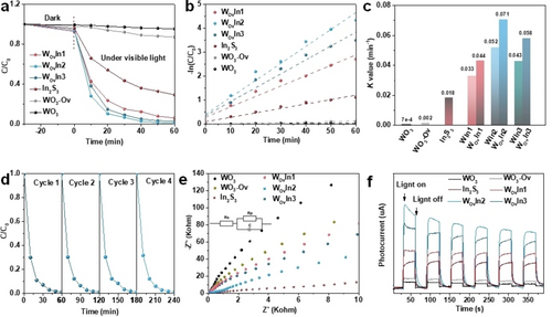
Enhancement in photocatalytic and photoelectrochemical performance after Ovs implantation. a) Photocatalytic degradation of RhB under visible-light irradiation over WO3, WO3-Ov, In2S3 and WO3-Ov/In2S3 samples. b) Pseudo first-order kinetics fitting. c) Comparison of rate constants (K, min−1) for different samples. d) Stability of photocatalytic RhB degradation of WOvIn2 sample. e) EIS spectra of WO3, WO3-Ov, In2S3 and WO3-Ov/In2S3 samples. f) Transient photocurrent spectra of WO3, WO3-Ov, In2S3 and WO3-Ov/In2S3 samples.
Density Functional Theory (DFT) Calculations
In order to unveil the effect of Ovs in the photocatalytic reaction, the related DFT calculation was carried out. As shown in Figure 5a, the partial density of states (PDOS) of WO3-Ov at Ef demonstrates increment compared with WO3 without Ovs, and the metallicity of WO3-Ov is enhanced. It can be manifested that the W-5d and S-3p orbital overlap and hybridize to form covalent bond. W−S chemical bonds at the heterointerface can act as specific “bridge” to accelerate charge transfer between In2S3 and WO3-Ov. Moreover, to visualize the charge transfer at the WO3/In2S3 interface, the calculated charge density difference was employed to trace the electron transfer behavior. The charge accumulation and depletion are denoted in yellow and blue regions, as shown in Figure 5b and Figure S36a, where substantial charge transfer at the WO3-Ov /In2S3 interface can be observed.22 From the Bader charge analysis,40 In2S3 transfers 1.342 e− to WO3-Ov, verifying that the charge transfer at the interfaces makes the heterostructure structures tighter, and is consistent with the experimental results. The planar-averaged differential charge density as a function of z for WO3-Ov/In2S3 is depicted in Figure S36b. The charge transfer at the heterointerface would subsequently induce the internal electric field in WO3-Ov/In2S3 heterostructure and further efficiently steer the separation of photogenerated charge carriers. In order to further investigate the spatial distribution of photogenerated electrons and holes and visualize the impact of surface Ovs, additional first-principles calculations were conducted. Our findings indicate that WO3-Ov generates photogenerated electrons from CB, which can subsequently be transferred to VB of In2S3 to combine with the photogenerated holes. The system of WO3-Ov/In2S3 exhibits spatial separation between the valence band maximum (VBM, Figure 5c) and conduction band minimum (CBM, Figure 5d), effectively suppressing electron-hole recombination. Compared with band-decomposed charge density distribution of WO3/In2S3 (Figure S37), the presence of Ovs leads to a greater electron localization of both VBM and CBM in the interface layer of the heterojunction, thereby forming a rapid charge transport channel between In2S3 and WO3-Ov.
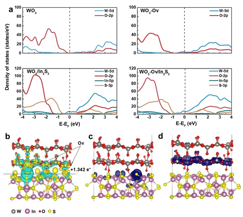
Calculated PDOS and differential charge density distribution of WO3-Ov/In2S3. Partial density of states (PDOS) of a) WO3, WO3-Ov, WO3/In2S3 and WO3-Ov/In2S3. b) Differential charge density distribution of WO3-Ov/In2S3 with Ovs. Isosurface level: 0.03 e/Bohr3. Blue and yellow colors denote electron excess and deficiency area, respectively. Band-decomposed charge density distribution of c) VBM and d) CBM for WO3-Ov/In2S3. The isosurface level is set as 0.001 e/Bohr3.
Fs-TAS Monitor Photogenerated Charge Dynamics
Furthermore, fs-TAS was performed to study the carrier dynamics (excited at 340 nm). As shown in Figure 6a, WO3 exhibits a distinct positive photoinduced absorption band (400–500 nm), which can be attributed to the signal from photogenerated holes.41, 42 Compared with pristine WO3, fs-TAS spectra of WO3-Ov show significant difference (Figure 6b) with the appearance of negative absorption bands above 500 nm. The negative absorption bands result from the re-trapping of the photoexcited electrons from CB to vacancy centers,42 indicating the kinetic behavior of photogenerated carriers can be effectively steered by Ovs defects. The fs-TAS spectra of WOvIn2 are shown in Figure 6c. The intensity of negative photobleaching signal gradually increases in 0.5 ps, then decays within 5 ps, which is related to the kinetic behaviors of photogenerated electrons. The fs-TAS spectra of WIn2 demonstrate difference with WOvIn2 (Figure 6d). Meanwhile, the pseudo color TA plots of WO3, WO3-Ov, WOvIn2 and WIn2 are shown in Figure 6e, respectively. Furthermore, the decay curves of WO3-Ov and WOvIn2 at 598 nm were recorded and fitted by a two-exponential function to investigate the kinetics of photogenerated electrons (Figure S38), where the short time τ1 and the long time τ2 correspond to photogenerated electrons trapped by the shallow and deep trapping states, respectively.43, 44 Compared with WO3-Ov (τ1=0.65 ps, τ2=6.03 ps), the lifetime of WOvIn2 decreases (τ1=0.39 ps, τ2=3.16 ps), which can be inferred that an additional channel for electron transfer exists at the interface between WO3-Ov and In2S3, accelerating the relaxation process of electrons. To estimate the decay kinetics of photogenerated holes, time profiles of fs-TAS at 428 nm were probed. Compared with WO3-Ov (τave=194.4 ps) (Figure 6f), the average decay lifetime (τave) of WOvIn2 is prolonged to 528.1 ps (Figure 6g), suggesting that photogenerated holes in the composite possess much longer lifetime and higher priority to participate in photo oxidation reactions.45 As comparison, the τave of WIn2 is 265.9 ps (Figure 6h), shorter than that of WOvIn2, further suggesting the creation of Ovs prolongs the lifetime of the photo-induced holes, thus favoring the improvement in photocatalytic activity. The fitting results are summarized in Table S6 and S7, which confirms the formation of S-scheme charge transfer between WO3-Ov and In2S3. Based on the above analysis, the mechanism of Ovs in the S-scheme heterojunction can be proposed, as depicted in Figure 6i. Ovs can generate impurity trap states in WO3-Ov which partially trap photogenerated electrons, thus inhibit direct recombination of the photogenerated electrons and holes. After hybridizing with In2S3, a new interfacial electron transfer pathway may be generated, the electron transfer and migration can be promoted by the internal electric field at the interface.46 The rapid electron trapping as well as the fast charge separation at the interface of WO3-Ov/In2S3 suppress electron-hole recombination. In addition, the existence of Ovs narrows the band gap of WO3-Ov, resulting in the enhancement of light absorption and the increased number of photogenerated carriers to participate the reaction.
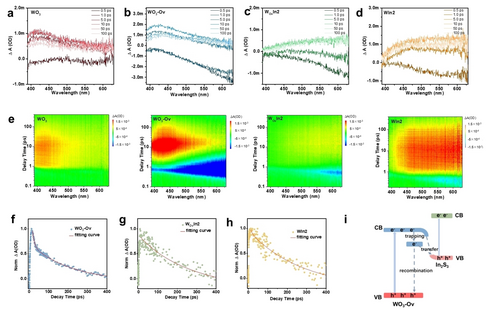
fs-TAS monitor the photogenerated charge dynamics. fs-TAS of a) WO3, b) WO3-Ov, c) WOvIn2 and d) WIn2. e) Pseudo color plots of WO3, WO3-Ov, WOvIn2 and WIn2. Normalized time profiles of fs-TAS at 428 nm of f) WO3-Ov, g) WOvIn2 and h) WIn2. i) Proposed photoinduced electron transfer and charge recombination route of WO3-Ov/In2S3 heterojunction.
Conclusions
In this work, WO3-Ov/In2S3 S-scheme heterojunction photocatalysts were successfully synthesized. The photocatalytic degradation performance of WO3-Ov/In2S3 S-scheme heterojunction was superior to that of single-component (35.5 and 3.9 times higher than WO3-Ov and In2S3, respectively.) and WO3/In2S3 heterojunction. The results of experimental characterizations and DFT calculations revealed that the microscopic environment and local electronic structure of S-scheme heterointerface were well engineered by Ovs. Meanwhile, Ovs favor the formation of a close interface connection. The influence of Ovs on charge transfer dynamics was investigated by employing fs-TAS. Ovs-induced trap states efficiently steered charge separation and triggered rapid charge transport channels at the heterointerface. Furthermore, Ovs improved light absorption, allowing for more photogenerated carriers. As a result, our study may contribute to a better understanding of Ov and the development of alternative S-scheme photocatalysts for advanced applications.
Acknowledgments
This work is financially supported by the Innovation and Technology Fund, Hong Kong, China (GHP/040/19SZ), the Hong Kong Polytechnic University (Project number: 1-ZE14), Photonic Research Institute, the Hong Kong Polytechnic University (Project number: 1-CD6V), and the Hong Kong Polytechnic University Shenzhen Research Institute, Shenzhen, China (Grant Code: the science and technology innovation commission of Shenzhen (JCYJ20210324141206017)).
Conflict of interests
The authors declare no conflict of interest.
Open Research
Data Availability Statement
The data that support the findings of this study are available from the corresponding author upon reasonable request.


