Illuminating the Electronic Properties of WS2 Polytypism with Electron Microscopy
Abstract
Tailoring the specific stacking sequence (polytypes) of layered materials represents a powerful strategy to identify and design novel physical properties. While nanostructures built upon transition-metal dichalcogenides (TMDs) with either the 2H or 3R crystalline phases have been routinely studied, knowledge of TMD nanomaterials based on mixed 2H/3R polytypes is far more limited. In this work, mixed 2H/3R free-standing WS2 nanostructures displaying a flower-like configuration are fingerprinted by means of state-of-the-art transmission electron microscopy. Their rich variety of shape-morphology configurations is correlated with relevant local electronic properties such as edge, surface, and bulk plasmons. Machine learning is deployed to establish that the 2H/3R polytype displays an indirect band gap of . Further, high resolution electron energy-loss spectroscopy reveals energy-gain peaks exhibiting a gain-to-loss ratio greater than unity, a property that can be exploited for cooling strategies of atomically-thin TMD nanostructures and devices built upon them. The findings of this work represent a stepping stone towards an improved understanding of TMD nanomaterials based on mixed crystalline phases.
1 Introduction
Many of the remarkable electronic and optical properties exhibited by transition-metal dichalcogenide (TMD) materials can be traced back to the underlying periodic arrangements of their layers, the so-called stacking sequences.[1, 2] Therefore, identifying and controlling these stacking sequences provides a powerful handle in the quest to design novel TMD-based nanostructures with tailored functionalities.
The most common stacking sequences present in TMDs are the 2H and the 3R polytypes.[3-5] The 2H phase belongs to the space group P63/mmc and has a unit cell composed of a bilayer following the AA′ stacking sequence, a configuration characterized by an inversion symmetry.[6] The 3R phase belongs instead to the space group R3m and is defined by a bilayer with an AB stacking sequence, which as opposed to the 2H phase does not exhibit inversion symmetry.[7] Both crystalline phases are known to display a semiconducting behavior.[8] While several studies of the structural, optical, and electronic properties of TMDs based on either the 2H or the 3R phases have been reported,[9-11] much less is known about how these properties are modified in the presence of a mixed 2H/3R polytypism.[12] Unravelling the implications of such polytypism in TMDs would open new avenues in applications from nanoplasmonics and nanoelectronics to catalysis.[13-15]
This work reports on the characterization of WS2 flower-like nanostructures (“nanoflowers”) composed by randomly oriented flakes (the “petals”) arising from a common point (the “stem”). These WS2 nanoflowers display a rich variety of shape-morphology configurations, such as lying petals and edge-exposed standing petals. Together with their polytypism, this unique feature turns these nanostructures into an ideal laboratory for the study of the modifications of local electronic properties in WS2.
First of all, aberration-corrected scanning transmission electron microscopy (AC-STEM)[16] is used to reveal the presence of the 2H/3R polytypism in these nanostructures. Then, the nature of their edge, surface, and bulk plasmonic excitations is fingerprinted by means of spatially-resolved electron energy-loss spectroscopy (EELS).[17, 18] The origin of relevant features in the EELS spectra is traced back to specific structural characteristics of the nanoflowers, and in particular one can identify contributions associated to the surface and interlayer couplings as well as to the edges of the WS2 petals. The combination of EELS measurements with machine learning is then exploited to chart the ultra-low-loss region () and determine that the 2H/3R polytype of bulk WS2 exhibits a semiconductor behavior with an indirect band gap of value of .
Further, EELS spectra recorded in a monochromated TEM[19] are used to demonstrate the presence of energy-gain peaks in the nanoflowers. These features could be associated with the interactions of collective excitations in the material, such as plasmons, or excitons, with the fast electrons from the beam. Remarkably, for specific nanostructures these energy-gain peaks can become more intense than their energy-loss counterparts, revealing the presence of an underlying mechanism whereby the beam electrons are on average accelerated after crossing the specimen. Such a remarkable feature could be exploited to develop novel cooling strategies for atomically thin TMD nanostructures and for the devices built upon them.
1.1 Mixed 2H/3R Polytypes in WS2 Nanoflowers: Fabrication and Structural Characterization
Figure 1a displays a schematic diagram summarizing the synthesis of the WS2 nanoflowers. These nanostructures were directly grown onto a microchip made of silicon as a frame with a silicon nitride (Si3N4) window in the middle (see Figure 1b).[20, 21] First, tungsten trioxide (WO3) powder (50 mg) was dispersed in 1 mL of isopropanol (ISO). Second, a few droplets of the mixed WO3 and ISO were deposited onto the microchip using a pipette (Figure 1c). As indicated in Figure 1a, a crucible holding 400 mg of sulfur (S) was placed upstream from the microchip in the low-temperature region of the three-zone furnace. An argon gas flow was used both to prevent oxidation as well as to transport the sulfur vapor to the microchip. Further details of the growth procedure can be found in the Supporting Information.
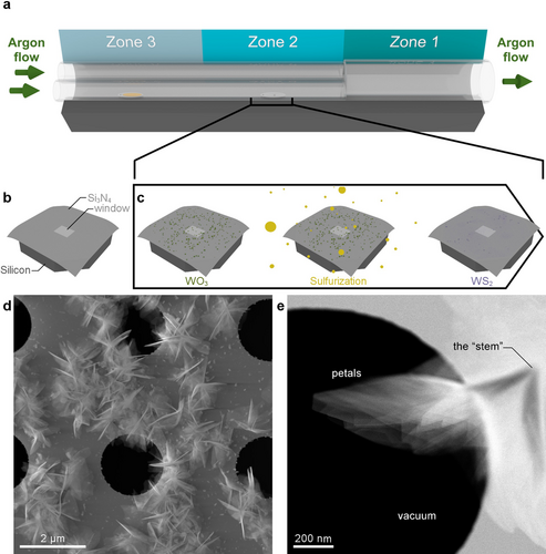
Figure 1d displays low-magnification annular dark-field (ADF) scanning transmission electron microscopy (STEM) images of the as-grown WS2 nanostructures. It is observed that the nanostructures exhibit flower-like morphologies composed by randomly oriented flakes (the “petals”) arising from a common point (the “stem”), see Figure 1e. The chemical composition of the WS2 nanoflowers was confirmed by means of energy-dispersive X-ray spectroscopy (Figure S3, Supporting Information).
Figure 2a,b displays respectively low-magnification ADF- and bright-field (BF-) STEM images of the tip region of one representative WS2 petal. The variations in image contrast indicates the presence of terraces with a different number of layers each, and thus of different thicknesses ranging from 2 nm up to 30 nm. Figure 2c then displays the atomic-resolution ADF-STEM image corresponding to the same petal. The petal has been oriented along the [0001] direction in order to ascertain the underlying crystalline structure. Each bright spot corresponds to an atomic column that is composed of alternating tungsten (W) and sulfur atoms.
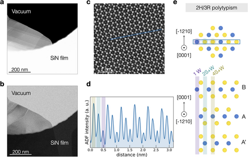
Based on the observed atomic arrangement, a hexagonal honeycomb with an atom in its center, the atomic-resolution image appears to suggest a 3R phase (Figure S4b, Supporting Information). However, the ADF linescan extracted from the atomic resolution image across six lattice points (Figure 2d) indicates a threefold periodicity which is inconsistent with the 3R phase.
Such periodicity suggests instead a layer stacking order of the type BAA′, characteristic of a mixture of the 2H (AA′) and 3R (AB) phases.[22] As displayed by the characteristic unit cell of polytypic 2H/3R (Figure 2e), the stacking sequence exhibits a broken inversion symmetry. Such polytypism has already been reported in related material like MoS2.[12] As mentioned above, the 2H and 3R phases in their bilayer form are characterized by different stacking sequences, namely AA′ and AB (Figure S4, Supporting Information). In the 2H phase, the W atom is aligned with the S one and the two layers exhibit inversion symmetry. In the 3R phase instead, the W atom is staggered over S, resulting in a stacking sequence lacking inversion symmetry. Therefore, a mixture of the two phases follows the BAA′ sequence, where the third layer is staggered with the S atoms over the W atoms of the second layer.
The area measured has a thickness of around 5 nm, which is equivalent to around 5 layers. The smallest thickness of any region in the specimen is found to be around 3 layers. ADF line profiles taken at different locations of other petals, corresponding to both single terraces and the transition region between terraces, exhibit in all cases the characteristic threefold periodicity of the 2H/3R polytype (see Figures S5 and S6, Supporting Information).
2 Fingerprinting Electronic Excitations with Spatially-Resolved EELS
The nature of collective electronic excitations such as surface and edge plasmons arising in the 2H/3R polytypism is investigated by means of spatially-resolved EELS. Figure 3a,b displays BF- and ADF-STEM images of horizontal WS2 flakes (the nanoflower petals) overlapping among them. Some of these petals are composed by terraces of different thicknesses, as indicated by the contrast variations in the ADF-STEM image, Figure 3b. Since these petals are suspended on vacuum, it is possible to characterize their edge, surface, and bulk plasmons while reducing the contribution from coupling effects related to the nanostructure support film. It should be emphasized that, in this specific geometric configuration, the incident electron beam direction is close to the c-axis of the WS2 petals.
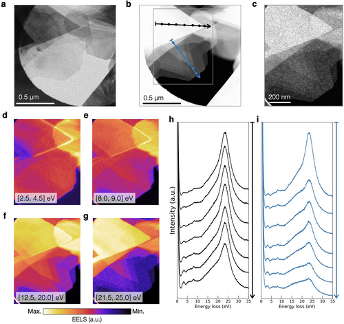
Figure 3c displays the spatially-resolved EELS map recorded in the region marked with a grey rectangle in Figure 3b, where each pixel corresponds to the intensity of an individual EEL spectrum. Figure 3d,g displays the intensity maps associated to the same EEL signals now integrated in specific energy-loss windows: [2.5, 4.5], [8, 9], [12.5, 20], and [21.5, 25] eV respectively. In these maps, the brighter regions highlight the dominant features appearing for each specific energy-loss range.
To better isolate the main features displayed by Figure 3d,g, representative EEL spectra associated to locations along the horizontal petals indicated in Figure 3b are presented in Figure 3h,i. A common feature of the two sets of spectra is the appearance of a prominent peak around 23 eV that can be associated with the WS2 bulk plasmon.[23] The intensity of this peak decreases as one moves from thicker towards thinner regions, following the directions of the arrows in Figure 3b. This effect is particularly marked in Figure 3i, corresponding to a petal composed by terraces of different thicknesses.
From the intensity map corresponding to energy losses integrated between 12.5 and 20 eV, Figure 3f, one observes a significant contribution arising from the regions constituted by two different overlapping petals. The individual spectra display indeed a shoulder-like feature located around 17 eV, which becomes more marked in the thinner regions. The free-electron gas dielectric response theory predicts that the surface plasmon energy, , should relate to that of the bulk one, Ep, by . In the present case, this prediction corresponds to around , consistent with the experimentally observed value and confirming the surface plasmon nature of this shoulder-like feature.[9]
The individual spectra in Figure 3h,i also display less intense peaks located at energy losses around 3 and 8 eV. From the integrated EELS maps of Figure 3d, one observes that the 3 eV peak can be mainly associated to the edges of the WS2 petals. Indeed, the largest signals in this energy-loss window arise from the tip of the edges and the adjacent regions. Further, it is observed that the peak at 8 eV receives its main contribution associated to the interlayer coupling between petals (Figure 3e). Indeed, this peak could be associated to the six π electrons (four of which are from the sulfur atoms) which are responsible for the interlayer interactions.[24, 25]
Figure 4a,b displays the ADF-STEM image and the corresponding spatially-resolved EELS map of another representative WS2 nanoflower composed now by both flat and tilted WS2 petals. In the latter case, their c-axis is close to being perpendicular to the direction of the electron beam. Figure 4c,d compares the energy-loss functions for the locations indicated in Figure 4b and recorded along a series of flat and tilted WS2 petals respectively. Spectra 6, 9, and 10 in Figure 4b are recorded in vacuum but close enough to the petal (aloof configuration), in order to identify possible contributions from its surface plasmons. It is found that the 3 eV peak appears both in the flat and tilted petals, as well as in the vacuum location sp9. In the vacuum region close to the sample, a peak for energy losses of around 3 eV is observed, whose location shifts rightwards to 3.5 eV when moving from the non-penetrating (vacuum) to the penetrating (WS2 petal) locations. To identify the physical nature of this feature a first principle density functional theory calculation (DFT) had been carried out, see Section SE, Supporting Information. The resulting total density of states (DOS) of 2H/3R WS2 bulk is shown in Figure S7a, Supporting Information. By comparing the total DOS of W and S (Figure S7b,c, Supporting Information) one can see that the main contribution to the total DOS is attributed to the W atoms (Figure S7b, Supporting Information). In particular, it suggests that the peak around 3 eV is associated to electronic transitions from d states of W to unoccupied d states of W (see Figure S7, Supporting Information).
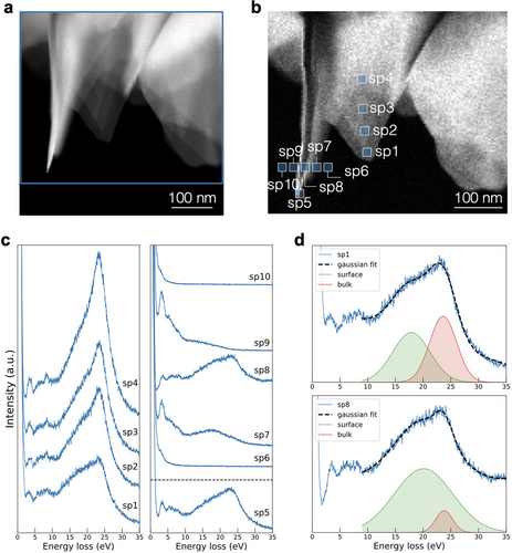
Concerning the higher-energy peaks, one finds that the tilted petal configuration induces a strong coupling between the surfaces which results in a split of the 17 eV surface mode into a peak at around 20 eV and a forest of peaks between 5 and 15 eV. In Figure 4d, a two-Gaussian model fit has been performed to sp1 (flat) and sp8 (tilted) in the range between 10 and 35 eV. The two resulting Gaussian distributions can be associated with the contributions from the bulk and surface plasmons and show how in the latter case the surface contribution at 17 eV blueshifts towards around 20 eV while becoming more marked as compared to the bulk one. Related phenomena have been reported in the case of WS2 nanotubes with very small radii.[23, 26]
3 Band Gap Determination of Polytypic 2H/3R WS2 from Machine Learning
The profile of the low-loss region of EEL spectra contains valuable information concerning the magnitude and type of the band gap. Exploiting this information requires the subtraction of the zero-loss peak (ZLP) contribution. Here the band gap of polytypic 2H/3R WS2 nanoflowers is investigated by means of a recently developed model-independent method based on machine learning.[27] This approach, developed in the context of high energy physics,[28] combines artificial neural networks for an unbiased parametrization of the ZLP profile with a Monte Carlo sampling for a faithful uncertainty estimate.
The original and subtracted EEL spectra corresponding to a representative location of a petal (labelled 5) and indicated in Figure S8, Supporting Information, are displayed in Figure 5a together with the calculated ZLP. This location corresponds to a relatively thick region where bulk behavior is expected. The uncertainty bands indicate the 68% confidence level intervals associated to the ZLP prediction and the subtracted spectrum. A functional form of the type is then[29] fitted to the subtracted spectrum ensuring that all relevant sources of uncertainty are considered. The results of such a fit are displayed in the inset of Figure 5a.
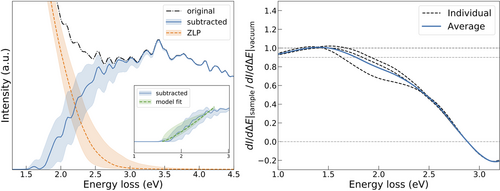
Figure 5b displays the ratio of the EELS intensity derivative, between the specimen spectrum and the corresponding vacuum average. This ratio highlights how for energy losses of 1.8 eV the two profiles start to differ, indicating the onset of the inelastic contributions to the spectra. The best-fit model values are for the band gap value and for the exponent. The latter result favors an indirect band gap, for which is theoretically expected. The obtained value and nature of the band gap of bulk WS2 is consistent with previous determinations in the literature.[8, 14] Statistically comparable results for the model fits are obtained for other locations in Figure S8, Supporting Information.
4 Energy-Gain Peaks in EEL Spectra
Additional high-resolution EELS measurements in these nanostructures were carried out using a monochromated electron microscope (see the Experimental Section). Figure 6a displays the ZLP profile acquired in the vacuum; its full width at half maximum (FWHM), indicating the spectral resolution under these operational conditions, is 57 meV. The resulting EELS spectra recorded at three representative petals of the WS2 nanoflowers are shown in Figure 6b–d. Each of these spectra corresponds to petals (displayed in the insets) characterized by different shape-morphology configurations: a flat petal tip (Figure 6b); a slightly bended petal (Figure 6c); and a completely bended petal (Figure 6d), respectively, where the darker contrast indicates bended regions.
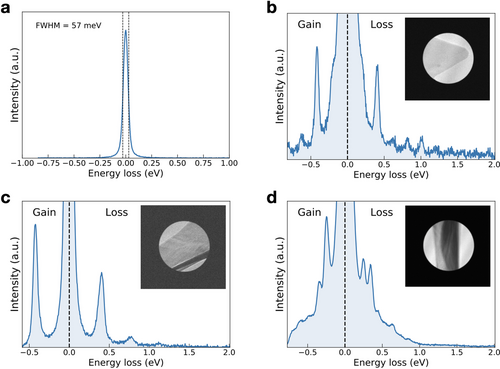
These spectra exhibit both energy-gain () and energy-loss () peaks, distributed symmetrically about . The spectra in Figure 6b and 6c correspond to WS2 petals oriented randomly, with the former being flat and the latter somewhat bended. From Figure 6b one finds symmetric peaks at and ±0.6 eV and a shoulder-like structure at eV. A similar pattern is observed in the thicker, slightly bended specimen of Figure 6c, where again strong symmetric peaks are observed at eV but now the energy interval between the low-loss region peaks is around 0.4 eV. The spectrum displayed in Figure 6d corresponds instead to a completely bended petal. For this configuration, the symmetric peaks appear for and ±0.6 eV. Since the positions of these peaks does not correspond to the phonon resonances of WS2,[30] their origin could be associated to the interactions between the fast electron beam with the evanescent field that is created through the collective excitations of the WS2 nanostructures.[31] In this respect, work in progress based on ab initio calculations will shed more light on the underlying mechanism responsible for these gain/loss peaks.
The ratio between the gain and loss peak intensities, , is known to depend on the relation between the associated thermal energies.[32] From the spectra displayed in Figure 6b–d, one observes that this ratio is typically larger than one. Specifically, for the symmetric peaks closer to the ZLP in each spectrum, values of = 1.2, 1.6, and 1.5 are obtained, respectively. It is found that bended petals appear to exhibit larger gain/loss ratios than their flat counterparts. One should note that related features have been also observed in TMDs when studied by means of Raman scattering,[33] where anomalously intense anti-Stokes peaks with are reported. Such remarkable behavior could be exploited to develop novel cooling strategies for atomically thin TMD nanostructures and devices built upon them.
5 Conclusion
The understanding of the implications of unconventional mixed crystalline phases on the properties of TMD nanomaterials remains partially terra incognita. This work has presented the exhaustive characterization of WS2 nanoflowers which provide an ideal laboratory for the study of the modifications of local electronic properties of WS2, thanks to their mixed 2H/3R polytypism and rich variety of shape-morphology configurations. By means of state-of-the-art AC-STEM and EELS measurements, the nature of their edge, surface, and bulk plasmonic excitations has been fingerprinted and the origin of distinctive features in the EELS spectra has been traced back to specific structural characteristics of the nanoflowers.
Further, thanks to a recently developed ZLP subtraction method based on machine learning, it has been stablished that the 2H/3R polytype of bulk WS2 exhibits a semiconductor behavior with an indirect band gap of . Further, the presence of energy-gain peaks in the EELS spectra recorded in the WS2 nanoflowers has been demonstrated. It has been shown that these peaks are characterized by a gain-to-loss ratio , indicating an underlying mechanism whereby electrons are on average accelerated after crossing the specimen. Such a feature could be exploited to develop novel cooling strategies for atomically thin TMD nanostructures and devices built upon them. This work therefore represents a stepping stone in a program aiming to develop a systematic strategy for the controllable growth of TMD nanostructures characterized by mixed crystalline phases.
6 Experimental Section
Electron Microscopy Characterization
The low magnification ADF image in Figure 1d and the EDS maps shown in Figure S3, Supporting Information, were taken using a Titan Cube microscope operated at 300 kV. The ADF- and BF-STEM and the EELS measurements displayed in Figures 1e, 2a–c, 3, and 4 were taken using a JEOL ARM200F microscope with a cold field-emission gun operated at 60 kV. This microscope is equipped with an aberration probe corrector and a Gatan GIF Quantum spectrometer. The convergence and collection semi-angles were set to 30.0 and 66.7 mrad, respectively. The spectral resolution (FWHM of the ZLP) achieved under these conditions is around 450 meV. The measurements in Figure 6 were collected in an ARM200F Mono-JEOL microscope equipped with a GIF continuum spectrometer. The microscope was operated at 200 kV in TEM mode with the monochromator ON and the smallest slit of 0.1 µm inserted. The aperture of the GIF was set to 1 mm. Under these conditions, one achieves a spectral resolution (FWHM) of 57 meV. In TEM-EELS the angular distribution of the electrons entering to the spectrometer aperture is independent of the entrance aperture size. The angular distribution is controlled by the size of the objective aperture in the diffraction pattern formed in the back focal plane of the objective lens. For these measurements, an objective aperture of 40 µm was used, therefore the collection angle becomes around 6 mrad.
Acknowledgements
The authors are grateful to Emanuele R. Nocera and Jacob J. Ethier for assistance in installing an EELSfitter in the Nikhef computing cluster. They also acknowledge discussions with Javier Garcia de Abajo on energy-gain phenomena in TMDs. S.E.v.H. and S.C.-B. acknowledge financial support from the ERC through the Starting Grant “TESLA”, grant agreement no. 805021. L.M. acknowledges support from the Netherlands Organizational for Scientific Research (NWO) through the Topconsortia voor Kennis en Innovatie (TKI) program. The work of J.R. has been partially supported by NWO.
Conflict of Interest
The authors declare no conflict of interest.


