

Journal list menu

 Issue
Issuephysica status solidi c: Volume 12, Issue 3
Special Issue:E‐MRS 2014 Spring Meeting – Symposium H: ALTECH 2014, see further papers in Phys. Status Solidi A 212, No. 3 (2015)
251-326March 2015
Export Citations
Download PDFs
Cover Picture
Cover Picture: Phys. Status Solidi C 3/2015
- First Published: 09 March 2015
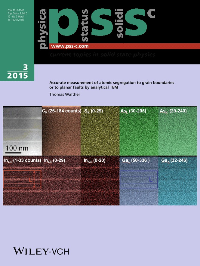
Measuring the areal density of solute atoms contained within a narrow planar fault, boundary or quantum well by standard analytical electron microscopy is possible but often yields a significant systematic underestimate. Improvements of detectors and/or aberration correction will improve resolution and counting statistics but not these systematic errors. Over the years, a new way to analyse series of analytical spectra by linear least-squares fitting approaches has been developed that eliminates this problem. The new method, presented by Walther on pp. 310–313, is more precise and reliable. The method has been shown to yield reliable segregation values down to a few percent of equivalent full monolayers, typically corresponding to <1 atom/nm2, and the precision can be directly estimated from the R2 parameter of the linear fit. It can be implemented in different illumination modes and is equally well suitable for X-ray and electron energy-loss spectroscopy. The figure displays an annular dark field image at the top left where three ultra-thin InAs quantum wells (with nominally 1.6, 1.8 and 2.0 atomic monolayers of indium) appear bright relative to the surrounding GaAs due to their enhanced scattering contrast. The coloured maps are intensity maps obtained for various X-ray lines, using a standard energy-dispersive Si:Li X-ray detector. From the linear fit of a plot of the As/In ratio as function of the width L of the sections around each quantum well, the total amount of indium in each quantum well could be determined to about ±0.1 monolayer precision.
Issue Information
Contents
Contents: Phys. Status Solidi C 3/2015
- Pages: 251-252
- First Published: 09 March 2015
Preface
Analytical techniques for precise characterization of nanomaterials
- Pages: 253-254
- First Published: 09 March 2015
Contributed Articles
Boron doped cubic silicon probed by high resolution X-ray diffraction
- Pages: 255-258
- First Published: 09 February 2015
Analysis of surfaces and materials
Near ambient pressure photoemission spectroscopy of metal and semiconductor surfaces
- Pages: 259-262
- First Published: 25 February 2015
XPS study of MoO3 and WO3 oxide surface modification by low-energy Ar+ ion bombardment
- Pages: 263-266
- First Published: 09 February 2015
Characterization of nanostructures
Dimensional and defectivity nanometrology of directed self-assembly patterns
- Pages: 267-270
- First Published: 25 February 2015
Characterization and simulation of optical absorption in Si nanocrystals
- Pages: 271-274
- First Published: 09 February 2015
In situ UHVEM irradiation study of intrinsic point defect behavior in Si nanowire structures
- Pages: 275-281
- First Published: 09 February 2015
Synthesis and utilization of LaVO4:Eu3+ nanoparticles as fluorescent near-field optical sensors
- Pages: 282-286
- First Published: 09 February 2015
Towards a standardised metrology for multi-scale characterisation of nanostructured durable hydrophobic coatings
- Pages: 287-291
- First Published: 25 February 2015
Study of thin films
Towards single-trap spectroscopy: Generation-recombination noise in UTBOX SOI nMOSFETs
- Pages: 292-298
- First Published: 23 January 2015
Control current stress technique for the investigation of gate dielectrics of MIS devices
- Pages: 299-303
- First Published: 09 February 2015
Micro-Raman spectroscopy as a complementary technique to high resolution X-ray diffraction for the characterization of Si1-xGex thin layers
- Pages: 304-309
- First Published: 09 February 2015
Accurate measurement of atomic segregation to grain boundaries or to planar faults by analytical transmission electron microscopy
- Pages: 310-313
- First Published: 23 January 2015
Ga+ implantation in a PZT film during focused ion beam micro-machining
- Pages: 314-317
- First Published: 09 February 2015
Multi-angle spectroscopic extreme ultraviolet reflectometry for analysis of thin films and interfaces
- Pages: 318-322
- First Published: 25 February 2015
Characterization of TiO2 antireflection coatings elaborated by APCVD for monocrystalline silicon solar cells
- Pages: 323-326
- First Published: 23 January 2015